
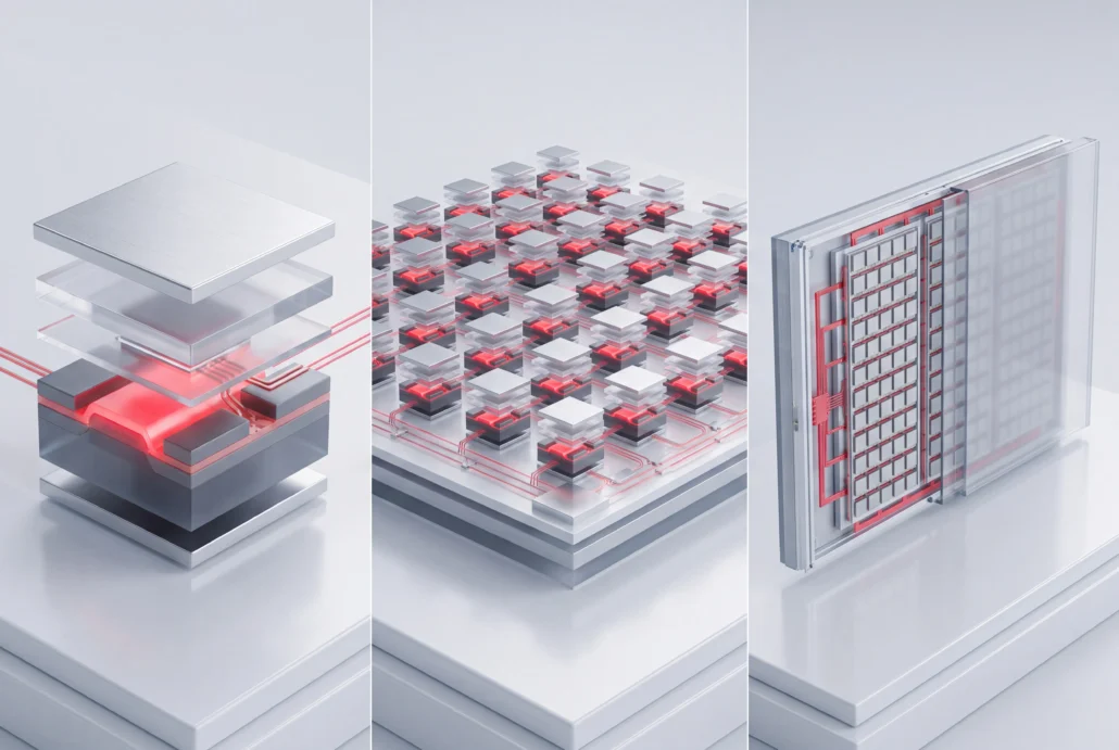
Display TFT simulation: from pixel device development to full panel design

A panel is millions of copies of one pixel device, and Silvaco follows that device from TFT simulation to the layout, extraction and verification of the full panel.

The pixel and the panel usually sit with different teams

Display development starts with one thin-film transistor or emitter and ends with a panel ready for manufacturing. OLED and microLED emitters, CMOS and TFT backplanes, flexible and stretchable substrates: each changes how the pixel device behaves. And every change has to hold up across the whole array.

Device engineers characterize the transistor. Panel designers take the array through capture, layout, extraction and verification, often in point tools from several vendors. You lose time at every handoff between the two. Eight of the world’s ten biggest display makers already do their device work in Silvaco TCAD.

One flow from the TFT to the signed-off panel

Your device team and your panel team work from the same models. What TCAD predicts
for the TFT is what your panel simulation runs on.

Input

Your pixel design

TFT, emitter and pixel circuit

01

Builds the TFT and emitter structures

02

Solves their device physics

03

Extracts TFT compact models

04

Runs pixel circuit design on the four-terminal TFT model

05

Simulates the full panel

06

Lays out pixels, with equal-resistance routing and fan-shaped connections

07

Pulls parasitics out of one cell or the whole panel

08

Signs off the layout at cell and panel level

Technologies and devices

Whichever backplane and emitter you’re weighing, the same tools cover it at device level
and at panel level. Much of that toolset was written for display work and nothing else. Its
proprietary functions take cost and time out of getting a panel to market.

Technologies

OLED, microLED and microOLED emitters, on backplanes built in CMOS or TFT.

Flexible and stretchable substrates as well, with the bending stress on each device modeled in simulation.

Device simulation

Process modeling and emulation build the structure. Drift-diffusion simulation solves it for a-Si, LTPS and IGZO TFTs and bulk CMOS. Bump and tail density-of-states modeling comes with it, along with mobility models specific to polysilicon and amorphous materials, and bending stress, hydrogen and grain effects.

Emitters cover LED, OLED, microLED and microOLED. Add a proprietary mobility model with self-heating, reverse ray tracing and TFT electrical stress effects. You run the device experiment before a wafer ever sees it.

Lasers, LEDs and silicon photonics

Choose from a wide set of TFT compact models: Silvaco’s proprietary four-terminal TFT model, and the RPI amorphous-silicon, polysilicon and universal organic TFT models.

Utmost IV extracts their parameters with several optimization algorithms, so the extraction strategy is yours to pick. Flat panel teams lean hard on Verilog-A parameter extraction, and it handles that too.

Design and layout

Device Explorer puts each device’s basic characteristics in the circuit schematic, where you can try them in simulation straight away. DRC assist, edit-in-place, connectivity highlighting, a short locator, layout versus layout and a cross-sectional viewer sit alongside.

Panel geometry has its own set in Expert: equal-resistance router, route along curve, pixel with frame, fan-shaped connections, clone wires and slot wires.

Panel-level verification

Hipex extracts parasitics fast and accurately for one cell or the whole panel, and SmartSpice Pro simulates the circuit at both scales.

Image retention and sticking get their own image quality features in SmartSpice. Then SmartDRC/LVS runs high-speed, high-accuracy physical verification, cell by cell and across the full panel.

Applications

Each one asks something different of the pixel.

Vehicle display

Panels for the car, from TFT backplane physics to full-panel sign-off.

Smartphone and tablet

Mobile panels built on OLED emitters and TFT backplanes.

Smart wearable, AR and VR

Small, dense displays, down to the liquid crystal on silicon pixels in AR headsets.

Transparent display

See-through panels, with device and panel simulated in the same flow.

Read further on TFTs, OLEDs and panels

TFT modeling, pixel-array simulation, OLED optics and liquid crystal on silicon, worked through in Silvaco webinars and Simulation Standard papers.

Presentation · PDF

February 2022

Display technology overview

The flat panel flow, from TFT and emitter device simulation to full panel design and verification.

Webinar · TFT modeling

February 2022

Learn How to Improve TFT-Based Flat Panel Designs with the Unique SmartSpice 4-Terminal TFT Model

Why a three-terminal compact model can only approximate a four-terminal TFT, and what a native four-terminal model gives modeling and design teams.

Webinar · Panel simulation

February 2022

Learn How Silvaco Flow Helps Designing and Simulating Pixel Arrays in Flat Panel Displays and Detectors

Schematic and layout, field-solver parasitic extraction, RC back-annotation into the netlist, and SPICE simulation of large pixel arrays.

ARTICLE · OLED OPTICS

February 2022

Optical Simulation of Organic Light Emitting Diode by Transfer Matrix Method with a Green's Function Approach and 2D FDTD

How light leaves a multilayer OLED stack, modeled two ways in one Simulation Standard paper.

Webinar · Liquid crystal

February 2022

Simulation and Analysis of Liquid Crystal on Silicon Pixels for Augmented Reality and Holography Applications

A phase-only LCoS spatial light modulator in simulation, and the problems that show up when you drive its pixels or shrink them.

More on power devices

Webinar

How to Eliminate Image Retention Issues with SmartSpice Flex Modeling

Webinar

Achieve Your Display Design Performance Edge Through Precision Parasitic Extraction

Webinar

How to Model and Simulate Flat Panel Pixel Arrays

Webinar

Reducing Organic LED Fabrication Time and Cost via Multi-Scale Flow Simulation

Webinar

TFT and OLED SPICE Modeling Using Utmost IV

Webinar

Device Simulation of Oxide Semiconductor TFTs: Device Modeling and Self-Heating Effects

Webinar

TCAD Solution for Flexible Display

Webinar

How FPD Designers Can Improve Productivity

Webinar

How TCAD Can Help You to Find The Right Material To Build Your Flexible Display

Article

Simulation of AlGaInP Multiple Quantum Well LED for Micro Display

Article

Channel-length Dependence of a-IGZO TFTs with Self-heating Effects

Article

3D TFT Simulation of Grains and Grain Boundaries

Article

Dynamic Analysis of Liquid Crystal Pixels

Article

Optical Simulation of Liquid Crystals in the In-plane Switching Mode

Article

TFT Panel Simulation Using SmartSpice Pro

Article

Edge Effect Analysis on TFT Devices Using 3D Numerical Simulation

Article

a-IGZO TFT Simulation

Article

Electrical Simulation of Liquid Crystals

Article

Hints, Tips, and Solutions – Calculate Light Extraction Efficiency in an OLED or LED with Pure Optical Simulation

Article

Modeling the Optical Response of Phonon-dressed Excitons in OLED Simulations

Examples

TCAD display application examples

Stuck on the TFT, the emitter or the panel?

Silvaco’s display specialists already work alongside display manufacturers on problems like
yours. Bring the one that’s costing you time. You’ll talk to someone who knows the panel as
well as the tool.

TFT and panel simulation, answered

What does a display development flow cover?

Everything between a single pixel-level device and a panel ready for manufacturing. TCAD simulates each TFT and emitter, and compact models carry that behavior into SPICE, where the panel is laid out, extracted, simulated and verified, cell first and whole array after. Silvaco covers both ends in one flow.

TFT simulation in Silvaco TCAD covers amorphous silicon, LTPS and IGZO TFTs alongside bulk CMOS backplanes, with density-of-states, mobility and stress models, and self-heating in oxide TFTs. At circuit level, customers already use the four-terminal TFT model for amorphous silicon, polysilicon, organic and metal-oxide TFTs, including LTPS, LTPO and flexible displays.

Many TFTs in production have four terminals, and a three-terminal compact model can only approximate one. Modeling teams end up building workarounds, and design teams inherit the approximation. Silvaco's proprietary four-terminal TFT model describes the device as it actually is, which gives both teams more room to work.

You simulate the pixel cell first, then the whole array. Parasitics are extracted at cell and full-panel scale, the RC elements are back-annotated into the netlist, and a fast SPICE simulator runs the panel as one circuit. Physical verification then checks the layout at those same two scales.

Dynamic effects in the TFTs cause it, hysteresis above all, and conventional SPICE models don't capture them. Silvaco's flex modeling reproduces those effects in SPICE. Your design team sees retention and sticking on the pixel circuit and can design them down before a panel is built.

Yes. Flexible and stretchable substrates are among the display technologies Silvaco supports, and device simulation models the bending stress on each TFT alongside hydrogen and grain effects. Silvaco has also published webinars on TCAD for flexible displays and on choosing the right material for one.

Expert

Layout for pixels and panels, including equal-resistance and curved routing.

SmartSpice

SPICE simulation with the four-terminal TFT model.

SmartSpice Pro

Circuit simulation at full-panel scale.

Hipex

Parasitic extraction from one cell to the whole panel.

SmartDRC/LVS

Physical verification from one cell to the whole panel.

Utmost IV

TFT compact model extraction and parameter optimization.

TCAD

The Victory tools for process and device simulation.

Automotive Semiconductor

Tools and IP for automotive semiconductor programs.