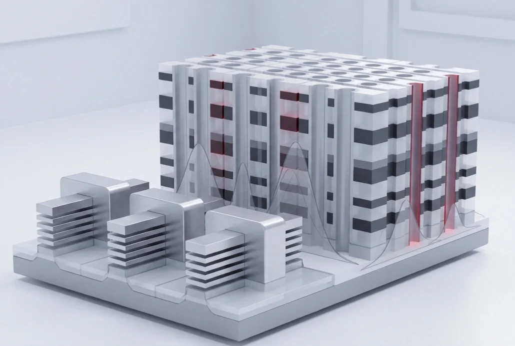
On an advanced CMOS or memory program, you can’t settle the process first and design the device afterward. A FinFET, a GAA nanosheet or a 3D NAND stack is a 3D object, and each etch and deposition shapes how it behaves electrically. A 2D shortcut throws away the very effects that make or break a new node.
Variation is the second problem. Every bit cell in an array is a copy of the same cell, so even a one-in-a-billion failure rate turns into lost yield. Simulate one cell or a slice, extrapolate, and you’re guessing. You need the full memory in view before silicon tells you the same thing at a far higher price.