Process Proximity Compensation: correct-by-construction OPC and mask pattern synthesis

Get a mask that prints your layout as drawn, computed from how your process actually moves each edge and checked in simulation first.

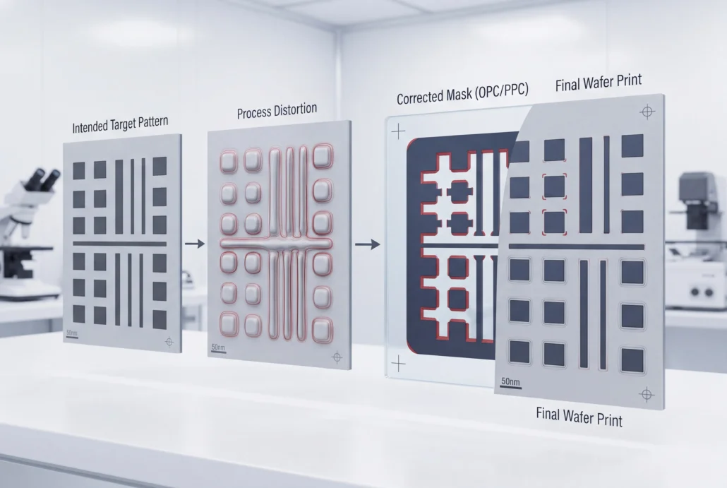
The mask you draw isn't the pattern you print

Silvaco’s Process Proximity Compensation (PPC) is a third-generation computational lithography suite, and its whole approach is correct-by-construction OPC. Optics, etch and the mask each pull a printed edge off target. PPC models all three, then computes the mask that cancels their combined shift. That gets harder at every node, because you’re expected to hold tighter dimensions without a longer mask cycle or a bigger OPC team. Silvaco acquired PPC, and the engineers behind it, from Cadence in March 2025.

Five stages from process data to a checked mask

Stage 1

Model calibration

Fit the models to measured data from your own process.

Tool: PPC

Stage 2

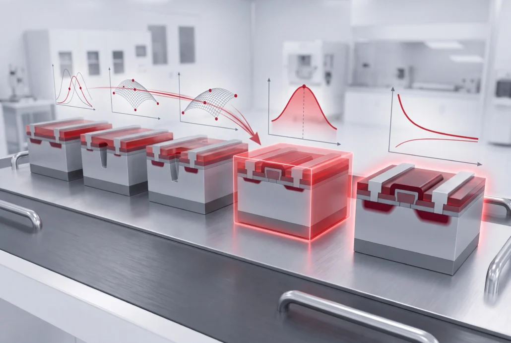
Predictive modeling and inversion

A physics-based predictive process model (PPM) that can be inverted, target to mask.

Tool: PPC

Stage 3

Correct-by-construction OPC

Compute the mask from the model instead of tuning it over repeated runs.

Tool: PPC; curvilinear mask synthesis in DimensionPPC

Stage 4

Source and SRAF optimization

Tune illumination and assist features with the mask to widen the process window.

Tool: PPC

Stage 5

Verification

Simulation checks the synthesized mask; mask rule checks confirm it can be made.

Tool: PPC; PPV and curvilinear MRC in DimensionPPC

From drawn layout to measured silicon, and back

What one layer measures on silicon improves the correction on the next.

In

Design intent

Your layout, as drawn

01

Lithography model

Aerial and resist image

02

PPC correction

Edges shifted to compensate

03

Mask data

Corrected and ready to write

04

Verification

Simulated back, rule-checked

05

Silicon result

Measured on the wafer

Out

Model calibration

Model refit against your data

The return arrow is the point. Refit the model to your own measurements and the fix lands on target.

Four jobs in one correction flow

Lithography simulation

See what a mask will print before you pay to make one. Physics-based litho models predict the aerial and resist image for each feature.

Process proximity correction

Correct the layout against the calibrated model, correct-by-construction instead of by trial and error. Source-mask optimization tunes the illumination with the mask, and hybrid SRAF placement widens the process window.

Model calibration

Fit the model to your wafer or CD-SEM measurements. Silvaco's predictive process model includes resist, etch and mask behavior as well as optics, so the dimension you correct to is the one that reaches silicon.

Verification and rule checking

Re-simulate the corrected mask and compare the printed contour with the target. Mask rule checks then confirm every shape is writable before
release.

Where holding the pattern gets hard

Same physics everywhere. What changes is which distortion eats your error budget.

Error budgets in nanometers

Dense arrays, mask rules bind first

Thick layers, etch-dominated edges

Uniformity across the panel

MEMS and sensors

Deep etches, extreme aspect ratios

Line width and via landing

Compound semiconductors

Resist on non-silicon substrates

Sidewall roughness costs light

Inside the PPC suite

Compute and cost of ownership

Synthesis and verification stay on general-purpose hardware, distributed over the cluster you already maintain. That keeps mask turnaround short and cost of ownership low.

Models

Production-proven lithography, etch and mask models. With all three in the correction, the target is the post-etch critical dimension your metrology reports, not the resist image.

Predictive process model

The PPM describes patterning physically, well enough to run in reverse. Give it the shape you need on the wafer and it works out the mask that will print it. That inversion is what correct-by-construction means in practice, and the optimization methods behind it are patented.

Source and SRAF optimization

Source optimization across multiple areas, and source-mask optimization, shape the illumination and the mask together. Hybrid SRAF placement adds the assist features. The aim is the widest process window your depth of focus allows.

Recipe creation

Build and optimize recipes in the GUI or in scripts. Someone new to a layer can start in the interface. The engineers who own the flow keep recipes as scripts, under version control, ready to rerun on the next tapeout. So the correction flow belongs to the team and doesn’t leave when one specialist does.

Layers where compensation earns its keep

Critical layers at advanced nodes

A few nanometers of edge-placement error can fail a layer, so no critical layer goes out uncorrected.

DRAM arrays

Dense layouts outgrow what Manhattan mask shapes can print, and curvilinear masks take over.

Etch-dominated layers

Etch bias moves the final edge further than the optics do.

Layers short on process window

The depth of focus the layer needs has to be won back through the source and assist features.

Mature and large-geometry nodes

The same models and flow keep established processes on target.

Published work on PPC

Conference talk · SURGE 2026

2026

Curvilinear OPC Applications

Nobue Kosa of Micron on moving several DRAM layers from Manhattan to curvilinear OPC with DimensionPPC: mask synthesis, simulation-based verification and curvilinear mask rule checks.

Press release · PDF

March 2025

Silvaco Expands Product Offering with Acquisition of Cadence's Process Proximity Compensation Product Line

Cadence's OPC suite, already in use at semiconductor companies, moved to Silvaco with the team that built it. Silvaco committed to continuity for existing customers' projects and support.

Bring the layer that won't close

Pick the one that keeps drifting off its CD target, or one you’re qualifying at a new
node, and talk it through with the team that builds PPC.

Questions about process proximity compensation

What is process proximity compensation?

Process proximity compensation adjusts a photomask so the pattern that reaches the wafer matches the layout. It works out how each feature will shift between mask and wafer, then pre-distorts the mask to cancel the shift. Silvaco's PPC suite is named for the job.

PPC is an OPC suite; optical proximity correction, or OPC, is the wider technique it belongs to. The difference is what gets modeled: PPC brings etch and mask effects into the correction alongside the optics. That points the result at the dimension you measure after etch, rather than just the printed image.

It means calculating a mask that prints correctly, rather than arriving at one by trial. Conventional model-based OPC moves edges, re-simulates and repeats until the print converges. PPC inverts a physics-based model of the patterning process, so it solves directly for the mask that hits the target.

SRAFs, or sub-resolution assist features, are small mask shapes too fine to print on their own. They change how the features next to them image, so those features keep their size across a wider spread of focus and dose. PPC places them with a hybrid method, in the same optimization as the illumination and the mask.

PPC is production-proven from large geometries through the most advanced processes. Micron has presented curvilinear OPC on several DRAM layers using DimensionPPC. For a specific node or layer type, ask our Technical Experts what PPC has already corrected on processes like yours.

It runs on general-purpose hardware. Each mask synthesis and verification step is broken into pipelined jobs that share out across your existing compute cluster. To size a job against your own layers, talk to our Technical Experts with the number of layers and the cluster you run.

Semiconductor design software models a device or circuit before it is manufactured: process and device simulation (TCAD), circuit simulation, parasitic extraction and physical verification. Silvaco builds all four.

Semiconductor design software models a device or circuit before it is manufactured: process and device simulation (TCAD), circuit simulation, parasitic extraction and physical verification. Silvaco builds all four.

Semiconductor design software models a device or circuit before it is manufactured: process and device simulation (TCAD), circuit simulation, parasitic extraction and physical verification. Silvaco builds all four.

Semiconductor design software models a device or circuit before it is manufactured: process and device simulation (TCAD), circuit simulation, parasitic extraction and physical verification. Silvaco builds all four.

Lithography

Computational lithography at Silvaco, including PPC and DimensionPPC.

TCAD

Process and device simulation for the steps after patterning, through to a working device.

FTCO

Fab Technology Co-Optimization: the same physics, AI-accelerated for fab and process engineers.