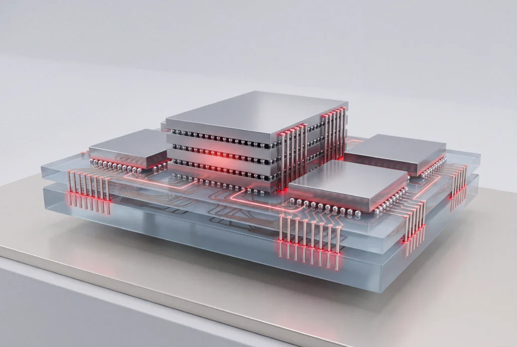
Advanced packaging: multi-die and 3D integration solutions

Advanced packaging makes dies you designed apart share heat, stress and wiring, so Silvaco starts at the physics underneath: 3D simulation of the stress a through-silicon via leaves in nearby silicon.

The package is now part of the design

Advanced packaging used to happen after the design was done. Now it’s where much of a product’s performance comes from, because the process node alone stopped delivering it. Stack dies in 3D and the wires get shorter, the footprint smaller, with through-silicon vias carrying signals from one die to the next.

The catch: each die was designed on its own. Put them in one package and heat moves between them. Vias and bonding push mechanical stress into the silicon beside them. The interconnect between dies adds resistance and capacitance of its own. Those effects cross team lines, sometimes company lines, so nobody owns them until something fails late.

Where Silvaco fits

Start at the via, where the package meets device physics.

Through-silicon via stress

Model the via in 3D in Victory Process and solve its thermo-mechanical stress before any stack is bonded.

Beyond one device

Chiplets, interposers, a multi-die stack: those questions start with your own structure. An application engineer can tell you what Silvaco covers for it.

Technologies and devices

What you can model today, at the via and around it.

3D TSV structures

In Victory Process, the through-silicon via is a true 3D structure, and its stress field is solved in 3D too.

The published work tests those finite-element results against the classical Lamé problem in elasticity, the textbook case for a via in an elastic medium.

Why the stress matters

Copper expands with heat far more than silicon does, so every thermal cycle loads the silicon around a TSV.

Stress-sensitive devices near the via can lose performance, and the 3D interconnect itself can crack.

Read the published work

Where Silvaco’s work on 3D integration is written up.

Webinar

February 2022

Thermo-mechanical Stress in Through-Silicon-Vias

Finite-element stress around a copper TSV, computed in 3D and cross-checked against a closed-form elasticity result.

Webinar

February 2022

Partitioning and DRC for 3D systems & ICs

How to partition a heterogeneous 3D system in space and run design rule checks on it, using the 3D IC software Silvaco built in an EU-funded project.

Describe your package

Tell us what you’re stacking or integrating and the effect you’re most worried about. We’ll match
it to the Silvaco tools that apply and say where their coverage ends.

What engineers ask about advanced packaging

What is advanced packaging?

Advanced packaging puts several dies in one package, side by side or stacked in 3D, connected through vias and bonds. Performance comes from how the dies are combined as much as from the node. Packaging becomes a design decision instead of the last step before shipping, since dies built separately now have to work as one.

Effects that used to stay inside one die now cross into its neighbors: heat, mechanical strain from vias and bonding, and the parasitics of every die-to-die connection. A single-SoC flow never had to model those. Each die is often owned by a different team, so you check the interactions package-wide, not die by die.

It means following heat through the whole stack instead of one die at a time. Stacked dies share heat paths, so a hot die warms the ones above and below it. Temperature shifts electrical behavior, and in a TSV it also drives stress, because copper and silicon expand at different rates.

Victory Process, at device level. It models a through-silicon via in 3D and solves for the stress in the silicon next to it. There’s no published Silvaco flow for multi-die or chiplet design. For anything past device physics, describe your structure to an application engineer and you’ll hear which tools fit it and which don’t.

Packaging adds interconnect the die never had: vias, bumps, redistribution layers and die-to-die wiring. Each adds RC that on-die extraction can't see, and at high frequency or high current those parasitics can rival the die's own. Hipex handles full-chip RC extraction on the die. For package-level parasitics, ask an application engineer.

Fab Technology Co-Optimization (FTCO) calibrates physics-based simulation against fab data to optimize a manufacturing process. Silvaco publishes it for front-end process and device work, not for packaging steps. If your question is about a packaging process such as via formation or bonding, raise it with an application engineer before assuming FTCO covers it.

AI and High-Performance Computing

Chips for AI and data-center compute, which drive most packaging demand.

InVar

Power, EM, IR-drop and thermal analysis

Hipex

Full-chip RC parasitic extraction.

TCAD

Victory Process, Victory Device and the rest of the TCAD family.