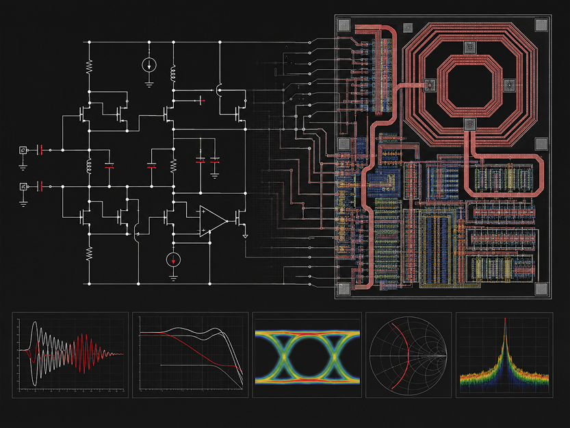
Analog and Custom IC Design

Silvaco’s analog IC design tools take your circuit from first schematic through layout, DRC and LVS, parasitic extraction and variation analysis to signoff, in one flow.

What analog IC design has to get right before tapeout

Analog IC design still happens one transistor at a time. You size and place each device, route each wire, and keep proving that the layout and the schematic are the same circuit.

It stays manual because analog IC design lives in what a digital flow abstracts away. Transistor matching matters. So does every wire, and the resistance and capacitance your analog layout adds. A bandgap reference or a PLL can look clean in schematic simulation and miss spec once the extracted parasitics go in.

So before tapeout, you check the layout against the foundry’s rules (DRC) and against the schematic (LVS). You extract the parasitics, simulate with them, then run the design across process variation to show it will yield. Caught in review, a mismatch costs a layout edit. Caught in silicon, it costs a re-spin. Silvaco covers those checks with Gateway, Expert, SmartDRC/LVS, Hipex, Jivaro Pro, Viso, PEX Certify and VarMan, plus SmartSpice and SmartView from Circuit Simulation.

One flow, not five handoffs

Schematic, layout, verification and extraction are built to work on each other’s data, so a mismatch shows up at the stage
that caused it. Not three stages later, where you’d have to trace it back.

01

Captures the schematic every later check is compared against

02

Draws the layout the masks are made from

03

Catches rule violations and layout-versus-schematic mismatches

04

Pulls parasitic resistance and capacitance out of the layout

05

Cuts the extracted netlist down to a size SPICE can run

06

Circuit Simulation

Simulates the circuit with its parasitics in

07

Circuit Simulation

Displays and measures the waveforms, so you see where a result misses spec

08

Shows whether the design yields across process variation

Sits beside reduction. When a post-layout result looks wrong, Viso shows which nets are responsible before you spend a simulation run finding out.

Checks the extractor itself. Compare two extracted netlists from different settings, versions, formats or tools, and see exactly where they disagree.

Upstream of simulation, Utmost IV characterizes your devices and generates the SPICE models SmartSpice runs on.

Tools for each stage of analog IC design

Start from the problem in front of you, whether that’s design entry, verification, parasitics or yield.

Design entry and layout

Capture the circuit and draw its layout in two editors that cross-probe with each other and with verification.

Gateway

Hierarchical schematic editor for analog, digital, mixed-signal and RF design, with symbols generated from your legacy netlists.

Expert

Hierarchical IC layout editor built for multimillion-transistor designs, with design rules checked while you draw. 

Verification and extraction

Every layout error costs less the earlier you find it, so check rules and connectivity before you measure what the layout adds electrically.

SmartDRC/LVS

DRC, LVS and netlist-versus-netlist checks, silicon-proven and foundry certified at Tower Semiconductor, X-FAB and UMC.

Hipex

Full-chip or selected-net RC extraction from hierarchical layouts, back-annotated onto your schematic netlist.

Parasitic reduction and analysis

At nanometer nodes, parasitics decide how your circuit behaves, and the extracted networks grow too large to simulate as they are.

Jivaro Pro

Parasitic reduction for up to 15X faster post-layout SPICE at the accuracy you set, from 65nm down to 2nm.

Viso

Checks crosstalk, net symmetry, delay and IR drop straight from the parasitic netlist, no simulation needed.

PEX Certify

PEX Diff and PEX Link qualify your extraction flow statistically, without long circuit simulations.

Variation and yield

Process variation at advanced nodes can sink yield, and traditional Monte Carlo is too slow to measure it at high sigma.

VarMan

Fast Monte Carlo, high-sigma and true-corner analysis, up to 30X faster than traditional Monte Carlo at the same accuracy.

VarMan XMA

Circuit Simulation

Monte Carlo yield analysis on the entire memory, not a slice or critical path extrapolated to the rest.

Where Circuit Simulation fits

Simulation runs twice in this flow, once on the schematic and again on the extracted layout.

SmartSpice

Runs your pre-layout simulations, then the post-layout ones on the reduced netlist

SmartSpice Pro

Gives you FastSPICE speed when a post-layout netlist is too large for full SPICE

SmartView

Every run's waveforms, measured and cross-probed with the Gateway schematic

Where analog IC design teams use this flow

Three kinds of work, each taken from what the product page says SmartSpice is for.

Analog and mixed-signal

Supported at every stage, from schematic capture to yield analysis

RF

Schematic capture, layout, physical verification and variation analysis for RF circuits

Memory

Hipex extraction for memory ICs, and full-memory yield analysis with VarMan XMA

Display and TFT

Equal-resistance routing for TFT and flat-panel layouts, with flat-panel rule checks

Power management

Physical verification for power-management designs

Standard cells and IO

Captured in Gateway and checked for statistical variation in VarMan

Accepted for signoff where the nodes are hardest

Micron, Nanya and PSMC have all signed recent multiyear agreements that take Silvaco’s sign-off accepted verification onto some of the
toughest process nodes in the industry. SK Hynix ran its HBM4E signoff with support from new capacity and performance work in Jivaro-
Pro-DX. And Silvaco EDA runs at six of the world’s ten biggest chipmakers.

DRAM

Customer · Jivaro Pro

eTopus

eTopus builds high-speed mixed-signal IP for data center and HPC chips. On its FinFET flow, a full post-layout simulation of a large block could run for weeks.

“…a full simulation on one of our blocks would run 20+ days. After using Jivaro Pro this runtime was reduced to 6 days while maintaining the designer’s accuracy requirements.”

Harry Chan, Founder and CEO, eTopus

Which step in your flow costs the most?

Bring the block you’re taking to tapeout next, or the step in your current flow that eats the most
time, and work through it with an application engineer on your own design data.

What engineers ask about analog IC design

What is analog and custom IC design?

Analog and custom IC design is chip design done at the transistor level. A designer captures the circuit as a schematic, draws its layout and verifies that the two match. Analog, mixed-signal, RF and memory blocks are built this way because device sizing, matching and layout parasitics decide how they behave.

A schematic editor, a layout editor, DRC and LVS, parasitic extraction, a SPICE simulator and a waveform viewer. At advanced nodes you'll also want parasitic reduction and variation analysis. In Silvaco's flow, those are Gateway, Expert, SmartDRC/LVS, Hipex, SmartSpice, SmartView, Jivaro Pro and VarMan, with Viso and PEX Certify for parasitic debug and extraction qualification.

Extraction calculates the resistance and capacitance your layout adds and writes them into the netlist. Hipex reads GDSII, cell netlists and rule-based tech files. Reduction then shrinks that extracted network so post-layout simulation finishes in reasonable time without losing accuracy. Jivaro Pro takes DSPF, SPEF and SPICE netlists from any extractor.

Yes. Expert imports existing Virtuoso technology data and links to Calibre Interactive and Calibre RVE when you verify. Gateway handles SPICE, CDL and Verilog netlists and supports HSPICE, OpenAccess and iPDKs. Jivaro Pro reads HSPICE, Spectre and Calibre View netlists, and Viso works alongside Virtuoso. Ask us to check your specific flow.

SmartDRC/LVS. It runs design rule checks, layout-versus-schematic and netlist-versus-netlist comparison on analog, digital and mixed-signal layouts, and scales across multiple CPUs. It’s foundry certified at Tower Semiconductor, X-FAB and UMC, and integrated with the Expert layout editor, which also links to Calibre if your foundry signs off there.

It means designing a circuit to meet spec across a real process’s variation, not only at typical corners. It becomes essential at advanced nodes and wherever a cell repeats thousands of times, like memory bit-cells, which may need verifying to 7 sigma and beyond. VarMan‘s high-sigma analyses get there with far fewer simulations than brute-force Monte Carlo.

More of AI-Driven Design

Circuit Simulation

SmartSpice, SmartSpice Pro, SmartView and the rest of the simulation tools this flow runs on

Lithography

Standard cell library creation, optimization and characterization

Design IP

License proven silicon instead of designing it, from Mixel MIPI PHY IP to foundation and system IP