Photonics and optoelectronics: image sensors, solar, lasers and silicon photonics

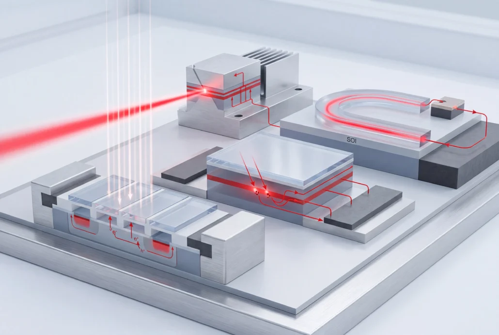
Every optical device, from a camera pixel to a silicon photonics laser, needs its light and its charge designed together. Silvaco simulates both in one coupled run, so you settle the device before you pay for the prototype.

Optoelectronics markets and the problem they share

Optoelectronic devices either take light in or give it out. Image sensors, CCDs and solar cells absorb it; lasers and LEDs emit it. CMOS image sensors are the largest of the four markets, pulled by smartphone cameras and reaching into high-end and scientific imaging. Solar cells answer the demand for renewable energy. And silicon photonics lasers and waveguides exist mostly to move data over fiber.

What ties them together is also what makes them hard: you can’t finish the optics and then start on the electronics. Your pixel has to catch light at very high sensitivity inside a battery-powered, often 3D-packaged part, where heat, IR drop and electromigration all eat into the same margin. A laser stands or falls on its optical modes. Chipmakers are taking that problem into simulation: ProMOS chose Victory TCAD in 2025 to develop silicon photonics devices, and Teledyne e2v widened its use of Victory TCAD for CMOS image sensors.

Where Silvaco fits

You start with the physics of one device and finish with a verified image sensor layout.
Photonic components get their own electromagnetic simulation alongside.

Input

Your optical device

A pixel, a solar cell, a laser or a waveguide

01

Builds the device structure the way your process would

02

Solves the optics and the electrical behavior together, laser cavity modes included

03

Extracts SPICE models for the image sensor's readout devices

04

Simulates the analog readout, large extracted designs included

05

Lays out the custom design

06

Checks the layout against the design rules and the schematic

Alongside

Electromagnetic simulation of photonic components

Device types and the optical
methods behind them

Each device couples light and charge its own way, so each gets
the optical method that fits it.

CMOS image sensors and CCDs

An image sensor is a pixel array plus its sense and control circuits, tuned for very high sensitivity. You take it from TCAD pixel design through SPICE simulation of the large extracted design to custom layout, then check electromigration, IR drop and thermal behavior for a 3D-packaged part. CIS-process PDKs are available from several foundries. CCDs run on the same TCAD suite.

Solar cells

Model silicon, thin-film and III-V cells, from interdigitated back-contact heterojunction designs to CIGS modules and GaInP/GaAs multi-junction cells with their tunnel junctions. You can take perovskite-silicon tandems through TCAD too, and a TCAD-to-SPICE flow takes a single cell up to panel level.

Lasers, LEDs and silicon photonics

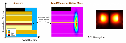
Laser and LED simulation covers edge-emitting and VCSEL lasers, LEDs and the waveguides of a fiber link, plus waveguide photodiodes and infrared and avalanche photodetectors. A mode solver and whispering-gallery mode analysis show how the cavity confines light. Ray tracing, the transfer matrix method, beam propagation and FDTD handle the rest of the optics, solved with the electrical model.

Applications

Four places where coupled simulation earns its keep.

CMOS image sensor development

Compare pixel structures in simulation, then design, lay out and verify the readout.

Solar cell device design

Test cell structures, silicon to tandem, with the optics and the carriers solved together.

Laser and VCSEL simulation

See the optical modes of an edge-emitting or vertical-cavity laser before the first die.

Waveguide and silicon photonics components

Simulate waveguides and photonic components before they reach a mask.

Customers and technical reading

Customer · Silicon photonics

February 2022

ProMOS Technologies

Chose Victory TCAD to develop its silicon photonics devices.

“The adoption of Silvaco’s Victory TCAD tools marks a significant step forward for ProMOS in developing next-gen photonic devices.”

Lynn Lin, Vice President, ProMOS Technologies

Customer · Image sensors

February 2022

Teledyne e2v

Took Victory TCAD further into its CMOS image sensor development.

“The Victory TCAD solution enables us to quickly analyze different pixel structures.”

Ana González Márquez, Director of Technology & Product Development, Teledyne e2v

Customer · Infrared detectors

February 2022

LYNRED

Runs Silvaco TCAD to tune infrared detector performance and shorten development cycles.

“Silvaco’s TCAD Solution is enabling us to lead advances on the infrared detector market by helping us fine-tune our designs and technologies to meet customers’ needs.”

Jocelyn Berhoz, PhD, Technical Expert, LYNRED

Customer · Optical sensors

February 2022

KODENSHI CORP.

Designs its optical sensor ICs in SmartSpice Pro.

“We decided to use SmartSpice Pro in order to be able to release high functionality, high value-added optical sensors in a short period of time.”

Hiroyuki Fukui, IC Design Division Senior Manager, KODENSHI CORP.

Laser and waveguide simulation in Silvaco TCAD

Presentation · PDF

February 2022

Optical Simulations Presentation

How Silvaco TCAD simulates devices that emit and absorb light, lasers and waveguides included.

Webinar · Image sensors

February 2022

Build Better Pixels Faster: TCAD-Powered Digital Twins for Next-Gen CIS

Use Victory TCAD, Victory DoE and Victory Analytics as a digital twin of your pixel, co-optimizing process, device and optics.

Webinar · Photonic ICs

February 2022

Accelerating Manufacturing-Aware Simulations for Photonic Integrated Circuits with FTCO™ and Digital Twins

Simulate photonic devices as they'll be manufactured, with line-edge roughness, sidewall angle and CD shift, from GDS import to digital twin.

Webinar · Solar

February 2022

Simulation of Silicon and Perovskite Based Tandem Solar Cells Using TCAD

Interdigitated back-contact cells, perovskite cells and silicon-perovskite tandems, modeled in TCAD.

Webinar · Optical methods

February 2022

Optoelectronic Simulation of Solar Cells, Waveguides, and LEDs

FDTD setup and output, worked through on solar cells, waveguides and LEDs.

More on power devices

Article · 2021

TCAD Modeling of Amorphous Selenium-based Avalanche Photon Detectors

Webinar · 2017

TCAD Simulation of Organic Optoelectronic Devices

Webinar · 2015

Solar cell modeling using TCAD and SPICE

Article · 2015

Optimizing Solar Cell Top Metal Contact Design Introduction

Article · 2013

2D IBC-SHJ Solar Cell Simulation and Optimization

Article · 2011

Design Consideration & Performance Analysis of MCT Based Dual Band (MWIR/LWIR) Photodetector

Article · 2010

Investigation of the SiGe Waveguide Photodiodes Using FDTD Method for High-Speed Optical Communication

Article · 2010

Modeling and Optimization of CIGS Solar Cell Module

Article · 2009

Textured Thin-film Solar Cell Simulation

Article · 2009

Third Generation Solar Cell Technologies: Localized Surface Plasmons

Article · 2009

Modeling of GaInP/GaAs DualJunction Solar Cells Including Tunnel Junction

Article · 2003

RPI VCSEL Model Released in SmartSpice

Put your device in front of our
application engineers

Which question does your lab keep answering too late? An application engineer will show
you where simulation settles it first, on a structure close to yours.

Photonics simulation questions

What is optoelectronics simulation?

It works out how a semiconductor device that absorbs or emits light will behave, before anyone builds it. An optical method, whether ray tracing, TMM, beam propagation or FDTD, is coupled to the device's electrical physics. That lets you tune image sensors, solar cells, photodetectors, lasers and LEDs in software rather than on test wafers.

In stages. TCAD builds and simulates the pixel, so you can compare pixel structures and geometries before fabrication. SPICE models and circuit simulation cover the analog readout, then custom layout and physical verification finish the design. Sensors often sit in 3D packages on battery power, so electromigration, IR drop and thermal analysis belong in the flow too.

CMOS image sensors and CCDs. Solar cells, from silicon and thin-film to III-V and perovskite tandems. Lasers, both edge-emitting and VCSEL, plus LEDs and OLEDs. Waveguides and waveguide photodiodes. Photodetectors, including infrared and avalanche types. Passive photonic components get electromagnetic simulation of their own.

A mode solver finds the optical modes a structure can support, which tells you how light is confined and guided in a waveguide or a laser cavity. For lasers, those modes set the far-field pattern, and whispering-gallery mode analysis covers cavities where light circulates around the edge. Silvaco's device simulation includes both.

Photonics simulation is the wider job: any device where light and charge meet, pixels and lasers included, usually simulated at device level in TCAD. The Photonics product family covers one part of it, the electromagnetic simulation of photonic components such as waveguides. Some devices need both.

Yes, and for most optical devices that's the point. Device simulation solves the optics self-consistently with the electrical physics, so carriers generated by absorbed light, or photons emitted by injected current, come out of the same run. Solar cells, image sensors and lasers all depend on that coupling.

Related IP

Photonics

The product family for photonic component simulation

XSim Photonics

Electromagnetic simulation for photonic devices

Victory Device

Optical and electrical device simulation, solved together

TCAD

Process and device simulation, from structure to SPICE model

Display

Pixel devices through to full panel design