

Requires: SmartSpice & Smartview
Minimum Versions: SMARTSPICE 3.16.12.R
The .BIASCHK3 statement is intended to track and report the maximum duration time (dt) when the voltage difference between the specified device
nodes or subcircuit terminals is larger than the user-defined reference voltage. It provides syntax to check specified terminals of chosen devices
and subcircuits by specifying subcircuit names, hierarchy xcalls, device names, device types and device model names.
This example input
deckshows how to use the “.biaschk3” statement to detect and report the maximum time duration when the monitored bias voltage is out of range.
This algorithm is based on a simple criterion:
- the “out-of-range” condition is defined by |Vbias| > |Vref|. The value of the user-defined reference voltage Vref must be specified in the .BIASCHK3 statement.
Statements:
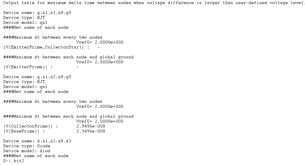
- .biaschk3 vref=2.0 devterminals=”ncx nei” devices=x1.x1.x8.q5
- .biaschk3 vref=2.0 devterminals=”nci nbi” devices=x1.x2.x8.q5
- .biaschk3 vref=2.0 devterminals=”nplusp nminus” devices=x1.x2.x8.d3
Output:
The
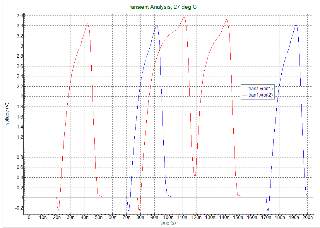
waveforms
show the simulated waveforms and the output table shows maximum delta time between nodes when voltage difference is larger than user-defined voltage level. Output log window shows part of
(pngview) log_info.png information
available in the log window for all the detected cases.
For full description, see the SmartSpice User’s manual section 3.13 .BIASCHK3.
Graphics
Input Files
B3_BJT_DIO_Device.in
*   EXAMPLE: TWO-BIT BJT ADDER AND .BIASCHK3 statement
*
.GLOBAL VCC
.SUBCKT NAND 1 2 3
Q1  9 5 1  QNL
Q2  9 5 2  QNL
Q3  6 9 8  QNL
Q4  7 6 10 QNL
Q5  3 8 0  QNL
D1  0 1  DIOD
D2  0 2  DIOD
D3  10 3 DIOD
R1  VCC 5  4K
R2  VCC 6  1.6K
R3  8   0  1K
R4  VCC 7  130
.ENDS NAND
*************  INA INB CIN OUT COUT
.SUBCKT ONEBIT  1   2   3   4   5
X1  1  2  7   NAND
X2  1  7  8   NAND
X3  2  7  9   NAND
X4  8  9  10  NAND
X5  3  10 11  NAND
X6  3  11 12  NAND
X7  10 11 13  NAND
X8  12 13 4   NAND
X9  11 7  5   NAND
.ENDS ONEBIT
.SUBCKT TWOBIT  INA1 INB1 INA2 INB2  BIT1 BIT2  CIN COUT
X1  INA1  INB1  CIN  BIT1 10   ONEBIT
X2  INA2  INB2  10   BIT2 COUT ONEBIT
.ENDS TWOBIT
VINA1  1 0  PULSE( 0 3 0 10NS 10NS 10NS 50NS)
VINB1  2 0  PULSE( 0 3 0 10NS 10NS 20NS 100NS)
VINA2  3 0  PULSE( 0 3 0 10NS 10NS 40NS 200NS)
VINB2  4 0  PULSE( 0 3 0 10NS 10NS 80NS 400NS)
X1   1 2 3 4   BIT1 BIT2  0  COUT    TWOBIT
RB1  BIT1 0  1K
RB2  BIT2 0  1K
RCOUT   COUT 0  1K
VCC  VCC 0  DC 5
.MODEL QNL NPN(BF=75 RB=100 CJE=1PF CJC=3PF)
.MODEL DIOD D
.TRAN 1NS 200NS
.SAVE V(BIT1) V(BIT2)
.OPTIONS RELTOL=0.001  NOMOD


.biaschk3 vref=2.0 devterminals="ncx nei" devices=x1.x1.x8.q5
.biaschk3 vref=2.0 devterminals="nci nbi" devices=x1.x2.x8.q5
.biaschk3 vref=2.0 devterminals="nplusp nminus" devices=x1.x2.x8.d3


.END
002_biaschk3
[an error occurred while processing this directive]