

Requires: SmartSpice & Smartview
Minimum Versions: SMARTSPICE 3.38.1.R
- DC Diode Analysis + Encrypted VA module.
This diode example shows how to run a DC sweep on this device using a Simple Verilog-A model and then with an encrypted model to get the same results. This shows the power of encryption to protect IP when multiple groups collaborate on a large circuit. The final circuit uses the encrypted model to show circuit performnce but will not show internal details of the model. Encyption through “sencrypt” program can be used to encrypt for various levels from individual lines, through various heiracheal levels like subcircuits to the full input deck contents depending on user requirements. Fabs can use this to protect more sensitive information but still allow customers to run circuit simulations.
The
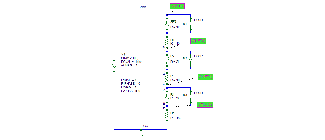
schematic
shows a simple tst circuit we will use to run the simulations.
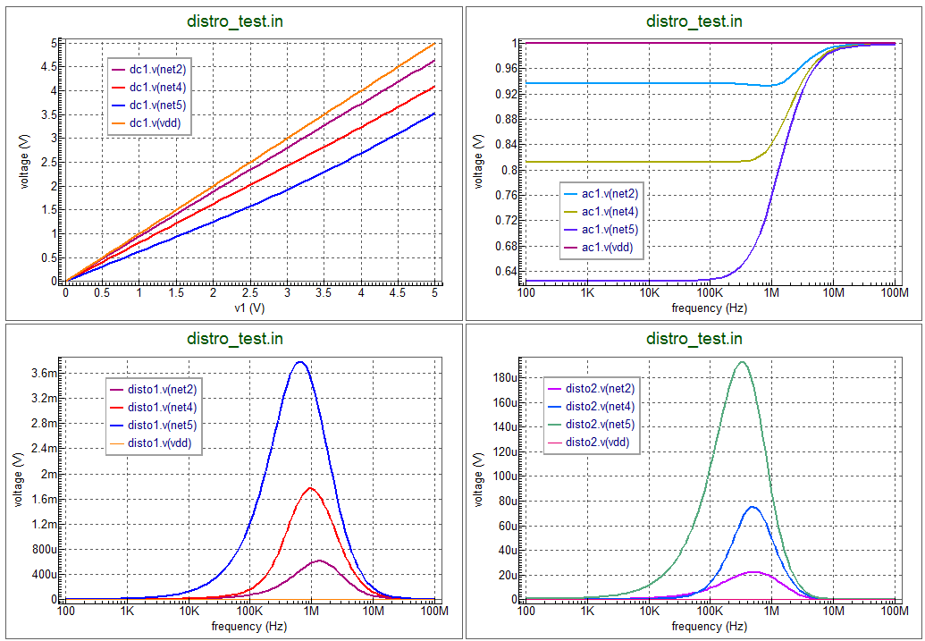
Having run the analysis you will get these set of response curves
plots
for the different analysis of .DC .AC and .Disto run.
Simple VA module simulation:
diode.in, diode.va
This shows for the limited parameter set and voltage range you can get the same response
from the Verilog-A module as with the inbuilt simple diode model.
Encrypted VA module simulation;
diode_encrypt.in, diode.en
The encryption was done on windows with command:
- …….\exe\sencrypt -at -skey=silvaco diode.va diode.en
NOTE:
To protect encrypted file no internal nodes are accessable to maintain confidentiality.
So you can see comparing waveforms you get the same results but in the encryted case information is hidden from the user.
Graphics
Input Files
distro_test.in
* Schematic name: distro_test
***********************************cs
RP3 VDD NET1 1k
V1 VDD GND DC dclev AC 1 DISTOF1 1 0 DISTOF2 1.5 0
D1 VDD NET1 DFOR
D2 NET2 NET3 DFOR
D3 NET4 NET5 DFOR
R1 NET1 NET2 10
R2 NET2 NET3 2k
R3 NET3 NET4 10
R4 NET4 NET5 3k
R5 NET5 GND 10k

.GLOBAL GND

.SAVE V(NET2) V(NET4) V(NET5) V(VDD)

.param dclev=0.0

.MODEL Dfor D (                 IS     = 6.241691E-4
+ RS    = 2.755033E-7     N     = 1.4816888       BV   = 11
+ IBV   = 1E-3            IK    = 3.5781E5        IKR  = 1.7E-3
+ JSW   = 1.233925E-9     AREA  = 7.5E-8          PJ   = 1.1E-3
+ CJ    = 1.01432E-3      PB    = 0.626873        MJ   = 0.373377
+ FC    = 0.5             CJSW  = 1.67236E-10     PHP  = 0.626873
+ MJSW  = 0.0748074       CTA   = 1.02351E-3      CTP  = 1.22727E-3
+ TLEV  = 1               EG    = 1.17            XTI  = 3
+ TRS   = 3.222E-3        TLEVC = 1               TPB  = 1.39435E-3
+ TCV   = -7E-4           TPHP  = 1.39435E-3      TREF = 25
+ LEVEL = 3               )

.DC V1 0 5 0.1
.AC dec 10 100 100Meg
.DISTO dec 20 100 100MHz

.save all(v)

.end
diode.in
*************************************************
* Verilog-A Diode module
* test to verify that op and dc analysis give
* the same result with the same input voltage
*************************************************

* Verilog-A device
*******************
.verilog "diode.va"

v1        11  0   dc 0.39
r1        11  1   1.0
YVLGdio   1   0   vlg_diode area=1

* smartspice internal device
*****************************
r1s      11  1s  1.0
Diode2   1s  0   my_diode

.op
.dc v1 0.3 0.4 0.001

*.print @YVLGdio[I(anode,cathode)] @YVLGdio[Vd]
*.print @Diode2[i]

.MODEL vlg_diode VLG MODULE=diode IS=1.E-7 N=.85 RS=0.01
*
.model my_diode D ( is=1.E-7  n=0.85 rs=0.01 )

*.option abstol=1e-12 reltol=1e-10

.end
diode.va
//******************************
//  Simple Diode Module        *
//*****************************cs

`include "discipline.h"
`include "constants.h"

module diode(anode,cathode);
 inout anode,cathode;
 electrical anode,cathode;

 parameter real area = 1 from (0:inf);
 parameter real is=1e-14 from (0:inf);
 parameter real n=1 from (0:inf);
 parameter real cjo=0 from [0:inf);
 parameter real m=0.5 from [0:inf);
 parameter real phi=0.7 exclude 0;
 parameter real fc=0.5 from (0:1];
 parameter real tt=1p from [0:inf);
 parameter real bv=1.0e+100 from [0:inf);
 parameter real rs=0 from [0:inf);

 real Vd, Id, Qd;
 real f1, f2, f3, fcp;
 real ibv;

 analog
   begin
     @(initial_step)
     begin
       f1 = (phi/(1 - m))*(1 - pow((1 - fc), m));
       f2 = pow((1 - fc), (1 + m));
       f3 = 1 - fc*(1 + m);
       fcp = fc*phi;
       ibv = is*bv/$vt;
     end

     Vd = V(anode,cathode);
     Id = I(anode,cathode);

// intrinsic diode.
     if (Vd < -5*n*$vt)
     begin
       if (Vd == -bv)
         I(anode,cathode) <+ -area*ibv;
       else
         if (Vd > -bv)
           I(anode,cathode) <+ -area*is;
         else
//           I(anode,cathode) <+ -area*is*(exp(-(bv + Vd)/$vt) - 1 + bv/$vt);
           I(anode,cathode) <+ -area*is*(exp(-(bv + Vd)/$vt) - 1 + bv/$vt);
     end
     else
       I(anode,cathode) <+ area*is*(exp((Vd - rs*Id)/(n*$vt)) - 1);

// capacitance (junction and diffusion).
     if (Vd <= fcp)
       Qd = tt*Id + area*cjo*phi*(1 - pow((1 - Vd/phi), (1 - m)))/(1 - m);
     else
       Qd = tt*Id + area*cjo*(f1 + (1/f2)*(f3*(Vd - fcp) +
                           (0.5*m/phi)*(Vd*Vd - fcp*fcp)));
     I(anode,cathode) <+ ddt(Qd);
   end
endmodule
diode_encrypt.in
*************************************************
* Verilog-A Diode module
* test to verify that op and dc analysis give
* the same result with the same input voltage
*************************************************

* Verilog-A device
*******************
.verilog "diode.en"

v1        11  0   dc 0.39
r1        11  1   1.0
YVLGdio   1   0   vlg_diode area=1

* smartspice internal device
*****************************
r1s      11  1s  1.0
Diode2   1s  0   my_diode

.op
.dc v1 0.3 0.4 0.001

*.print @YVLGdio[I(anode,cathode)] @YVLGdio[Vd]
*.print @Diode2[i]

.MODEL vlg_diode VLG MODULE=diode IS=1.E-7 N=.85 RS=0.01
*
.model my_diode D ( is=1.E-7  n=0.85 rs=0.01 )

*.option abstol=1e-12 reltol=1e-10

.end
027_DC_sweep_plus_Encryption
[an error occurred while processing this directive]027_DC_sweep_plus_Encryption
[an error occurred while processing this directive]