

Requires: SmartSpice & Smartview
Minimum Versions: SMARTSPICE 3.16.12.R
The .dcmatch analysis statement in SmartSpice can be used to vary device contributions to the total deviation of a dc circuits charateristics.
In this example a simple OpAmp circuit is used with the following element variations:
- Global: NMOS U0 = 10% PMOS U0 = 8%
- Local: NMOS – Vth0 PMOS – Vth0
- Element: R – r = 10%
The
input deck is a SPICE file containing the variation block definition.
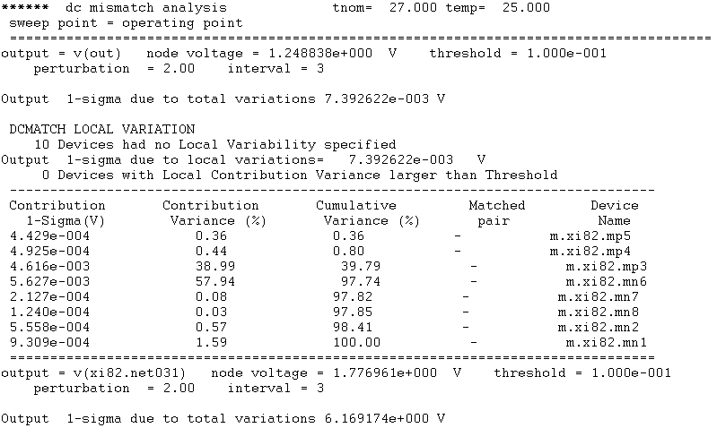
To run the simulation, Source the deck and press the green run button. When the simulation completes, the
results
are shown in SmartSpice log Window.
This shows the first output section due to the variation block in the
GUI window,
and is the first of 5 such reported variations in the output log.
Looking through the data printed in the output log you can see the variation applied and the influence on the circuit behaviour.
Graphics
Input Files
opampdcm.in
**
.GLOBAL gnda vdda
.PARAM vdd=2.5 vin=vdd/2 k=2

.subckt opamp gnda inn inp out vdda nmosbulk pmosbulk
mn1 net031 inn net044 nmosbulk modn L='k*0.5u' W='k*3.5u' M=4
mn2 net18 inp net044 nmosbulk modn L='k*0.5u' W='k*3.5u' M=4
mp3 net031 net031 vdda pmosbulk modp L='k*0.5u' W='k*4.5u' M=4
mp4 net18 net031 vdda pmosbulk modp L='k*0.5u' W='k*4.5u' M=4
mp5 out net18 vdda pmosbulk modp L=400e-9 W=10e-6 M=3
mn8 net0148 net0148 gnda nmosbulk modn L=3e-6 W=18e-6 M=5
mn7 net044 net0148 gnda nmosbulk modn L=3e-6 W=18e-6 M=2
mn6 out net0148 gnda nmosbulk modn L=3e-6 W=18e-6 M=12
ccomp out net058 9e-13
rcomp net18 net058 7e3
r0 net0148 vdda 1e6
.ends opamp

c0 in_neg 0 1m
c1 out 0 5e-12
r1 0 out 1e6
r0 in_neg out 10e6
xi82 gnda in_neg in_pos out vdda gnda vdda opamp
v2 0 gnda DC=0
v1 in_pos 0 DC=vin AC 1
v0 vdda 0 DC=vdd

.MODEL modp PMOS (  LEVEL   = 49   VERSION = 3.1
+ TNOM    = 27             TOX     = 4.E-9
+ XJ      = 1E-7           NCH     = 4.1589E17      VTH0    = -0.4215645
+ U0      = 119.2085214    UA      = 1.656038E-9    UB      = 1E-21
+ LWL     = 0              CAPMOD  = 2              XPART   = 0.5
+ CGDO    = 6.52E-10       CGSO    = 6.52E-10       CGBO    = 1E-12
+ CJ      = 1.156829E-3    PB      = 0.8604313      MJ      = 0.4161985
+ CJSW    = 1.800318E-10   PBSW    = 0.6161205      MJSW    = 0.2735145
+ CJSWG   = 4.22E-10       PBSWG   = 0.6161205      MJSWG   = 0.2735145 )

.MODEL modn NMOS (  LEVEL   = 49  VERSION = 3.1
+ TNOM    = 27             TOX     = 4.E-9
+ XJ      = 1E-7           NCH     = 2.3549E17      VTH0    = 0.3796589
+ U0      = 269.0634518    UA      = -1.188565E-9   UB      = 1.930877E-18
+ LWL     = 0              CAPMOD  = 2              XPART   = 0.5
+ CGDO    = 7.45E-10       CGSO    = 7.45E-10       CGBO    = 1E-12
+ CJ      = 9.725136E-4    PB      = 0.7292509      MJ      = 0.3610145
+ CJSW    = 2.269386E-10   PBSW    = 0.6351005      MJSW    = 0.1
+ CJSWG   = 3.3E-10        PBSWG   = 0.6351005      MJSWG   = 0.1 )

.variation
  .global_variation
     nmos modn vth0=0.07 u0=10 %
     pmos modp vth0=0.08 u0=8 %
  .end_global_variation
  .local_variation
     nmos modn vth0='1.234e-9/sqrt(get_E(W)*get_E(L)*get_E(M))'
+                 u0='2.345e-6/sqrt(get_E(W)*get_E(L)*get_E(M))' %
     pmos modp vth0='1.234e-9/sqrt(get_E(W)*get_E(L)*get_E(M))'
+                 u0='2.345e-6/sqrt(get_E(W)*get_E(L)*get_E(M))' %
     .element_variation
         R r=10 %
     .end_element_variation
  .end_local_variation
.end_variation

.dcmatch v(out) v(xi82.net031)  V(out,xi82.net031) i(v0) i(v2) THRESHOLD=0.1 FILE="filename" INTERVAL=3 PERTURBATION=2
.dc k start=1 stop=4 step=0.5

*.probe dcmatch_total

*.meas DC systoffset find V(in_pos,in_neg) at=2
*.meas DC dcmoffset find DCm_local at=2
*.meas DC maxoffset param='abs(systoffset)+3.0*dcmoffset'
*.meas DC dcm_mn2 find DCm_local(xi82.mn2) at=2

.TEMP 25
.option nomod nodeck nowarn dcon=1
.option post=2
.END