

Requires: Utmost IV, SmartSpice, SmartView
Minimum Versions: Utmost IV 1.10.6.R, SmartSpice 4.10.2.R, SmartView 2.28.2.R
This example describes how to extract a level 1 diode model given
typical forward and reverse current and reverse capacitance measurement
data. A diode is a device with two terminals (nodes), the anode (A)
and cathode (C). In forward operation, the anode bias is more positive
than the cathode and in reverse operation the inverse is true.
The project file
opt_ex05.prj
and the data file
diode.uds
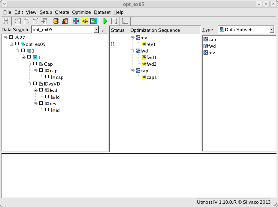
for this example should be loaded into your database. When opened, the
project will look as shown in
opt_ex05_01.png
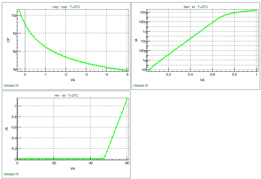
and when plotted, the example measured data will look as shown in
opt_ex05_02.png
.
The optimization sequence, which fully automates the extraction of this
level1 diode model example, has three sections. The objective of each section
is to isolate a device characteristic and then to optimize only those
model parameters which account for this device behavior.
The first section, takes the reverse current characteristic and extracts the
parameters
BV
and
IBV
associated with the reverse breakdown. Also included is the
RS
parameter representing the device series resistance.
The second section extracts the forward diode current parameters,
IS
and
N
. It also adjusts the series resistance parameter,
RS
, since the fit in the high forward current region is often more
important than that in reverse operation.
In the final section, the reverse bias capacitance parameters,
CJ0
,
MJ
and
VJ
are optimized.
Note that the
Levenberg-Marquardt
optimization method was used throughout this example, except for the
fwd1
optimization setup where a more advanced
Parallel-Tempering
optimization is required.
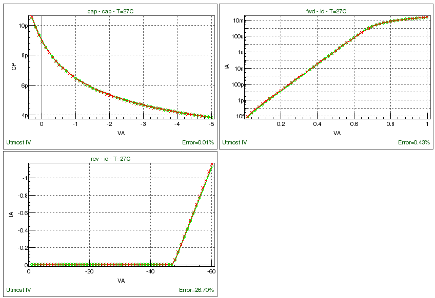
Once the sequence is complete, the final model fit is as shown in
opt_ex05_03.png
. The model card can then be exported into an external model library
file as shown in the output file
opt_ex05.lib.
Graphics
Files
opt_ex05.lib
.LIB demo

.MODEL dio D (
+LEVEL    = 1              IS       = 7.82198e-15    ISW      = 1e-18
+RS       = 10.8026        N        = 1.01199        BV       = 47.418
+IBV      = 0.00774265     CJO      = 8.91642e-12    VJ       = 1
+MJ       = 0.46959        FC       = 0.5            CJSW     = 1e-10
+VJSW     = 0.8            MJSW     = 0.3            FCSW     = 0.5
+AF       = 1              XTI      = 3              EG       = 1.17            )

.ENDL demo
opt_ex05.uds
Utmost IV CSV Data Logfile
Format Version 1
Copyright (c) 1984 - 2016 Silvaco, Inc. All rights reserved

DataSetStart

DataSetName, Cap
MeasurementType, LCR

BatchName, opt_ex05
WaferName, 1
DieName, 1
GroupName, 1, 0, 0.9
DeviceName, cap
Temperature, 27

FabDate, 24 Apr 2007
UserDate, 24 Apr 2007

WaferDiameter, 20
DieSize, 1, 1

NodeNames, A C

LCRSource, A, C, 1e+06, V, 0
LCRTarget, CP
Sweep, 1, V_LCR, LIN, 0.3, -5, -0.1, CALCULATED

Constant, V, C, 0, 0.0, 0.0

Function, VA, VC + V_LCR

Plot, cap, XY (LIN LIN), VA, CP

DataArray, CP
1.05231e-11    9.88825e-12    9.35945e-12    8.91e-12       8.52173e-12
8.18184e-12    7.88099e-12    7.6122e-12     7.3701e-12     7.15053e-12
6.95018e-12    6.76637e-12    6.59694e-12    6.44009e-12    6.29433e-12
6.1584e-12     6.03123e-12    5.91192e-12    5.79969e-12    5.69385e-12
5.59381e-12    5.49907e-12    5.40917e-12    5.3237e-12     5.24231e-12
5.16469e-12    5.09055e-12    5.01963e-12    4.95171e-12    4.88658e-12
4.82405e-12    4.76395e-12    4.70613e-12    4.65045e-12    4.59678e-12
4.54499e-12    4.49498e-12    4.44665e-12    4.39991e-12    4.35467e-12
4.31085e-12    4.26838e-12    4.22719e-12    4.18721e-12    4.1484e-12
4.11068e-12    4.07402e-12    4.03835e-12    4.00365e-12    3.96986e-12
3.93694e-12    3.90486e-12    3.87359e-12    3.84308e-12

DataSetFinish

DataSetStart

DataSetName, IDvsVD
MeasurementType, DC

BatchName, opt_ex05
WaferName, 1
DieName, 1
GroupName, 1, 0, 0.9
DeviceName, fwd
Temperature, 27

FabDate, 24 Apr 2007
UserDate, 24 Apr 2007

WaferDiameter, 20
DieSize, 1, 1

NodeNames, A C

Sweep, 1, V, A, LIN, 0.02, 1, CALCULATED, 50, 0.1

Constant, V, C, 0, 0.1, 0.0

Target, I, A

Plot, id, XY (LIN LOG), VA, IA

DataArray, IA
7.12711e-15    2.25709e-14    5.60342e-14    1.28546e-13    2.85664e-13
6.26115e-13    1.36382e-12    2.9623e-12     6.42597e-12    1.39312e-11
3.01938e-11    6.54322e-11    1.41788e-10    3.07239e-10    6.65746e-10
1.44257e-09    3.12583e-09    6.77316e-09    1.46763e-08    3.1801e-08
6.89067e-08    1.49305e-07    3.23495e-07    7.0085e-07     1.5181e-06
3.28701e-06    7.11084e-06    1.53541e-05    3.30205e-05    7.042e-05
0.000147653    0.000299865    0.000577358    0.00103123     0.00168884
0.00254339     0.00356595     0.00472245     0.00598302     0.00732423
0.00872852     0.0101828      0.0116775      0.013205       0.0147598
0.0163376      0.0179348      0.0195487      0.0211771      0.0228181

DataSetFinish

DataSetStart

DataSetName, IDvsVD
MeasurementType, DC

BatchName, opt_ex05
WaferName, 1
DieName, 1
GroupName, 1, 0, 0.9
DeviceName, rev
Temperature, 27

FabDate, 24 Apr 2007
UserDate, 24 Apr 2007

WaferDiameter, 20
DieSize, 1, 1

NodeNames, A C

Sweep, 1, V, A, LIN, -60, -1, CALCULATED, 60, 0.1

Constant, V, C, 0, 0.1, 0.0

Target, I, A

Plot, id, XY (LIN LIN), VA, IA

DataArray, IA
-1.13092       -1.0403        -0.949703      -0.859124      -0.76857
-0.67805       -0.587571      -0.497149      -0.406805      -0.316579
-0.22655       -0.136918      -0.0485385     -7.40165e-10   -6.21725e-15
-6.21725e-15   -6.21725e-15   -5.77316e-15   -5.77316e-15   -6.66134e-15
-6.66134e-15   -6.21725e-15   -6.21725e-15   -6.21725e-15   -6.21725e-15
-5.77316e-15   -5.77316e-15   -6.66134e-15   -6.21725e-15   -6.21725e-15
-6.21725e-15   -6.21725e-15   -6.21725e-15   -6.21725e-15   -6.21725e-15
-6.21725e-15   -6.21725e-15   -6.21725e-15   -6.43929e-15   -6.21725e-15
-6.21725e-15   -5.9952e-15    -6.21725e-15   -6.21725e-15   -6.21725e-15
-6.21725e-15   -6.21725e-15   -6.21725e-15   -6.21725e-15   -6.10623e-15
-6.10623e-15   -6.21725e-15   -6.10623e-15   -6.10623e-15   -6.10623e-15
-6.10623e-15   -6.10623e-15   -6.10623e-15   -6.10623e-15   -6.10623e-15

DataSetFinish