

Minimum Required Version: Guardian LVS 4.8.36.R
Guardian LVS can process specific SPICE elements, such as independent voltage/current sources, voltage/current-controlled switches and so on. They are ignored during the normal LVS process, but they can be compared between a pair of netlists, in order to verify if the converted schematic data is equivalent to the original one.
A check box Process specific SPICE elements is provided in the General page in the Project Settings dialog. It compares those specific SPICE elements as well as the normal device instances. The result of the comparison is reported in the log file and unmatched node reports.
If some independent voltage sources are included in the netlist, the parameter comparison should be executed for more accuracy. The parameter of independent voltage sources includes transient analysis source specifications, such as pulse, sin, and cos. To check those parameters, another option, Match transient source parameters, should be turned on. Any discrepancies are reported in the parameter error file.
See the example of the log file with specific SPICE elements in App_lvs1.log.
The actual steps of the operation to check the command behaviors are as follows:
1) Start Guardian LVS in the GUI mode.
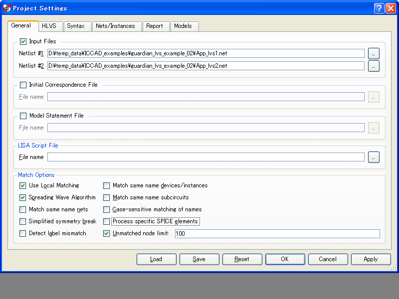
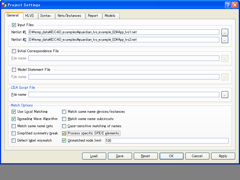
2) Select Setup->Project Settings command to show the Project Setting dialog (see Figure 1
).
3) Click the Reset button in the Project Settings dialog.
4) Turn on the Input Files check box in the General page, and set the following netlists as #1 and #2 netlists:
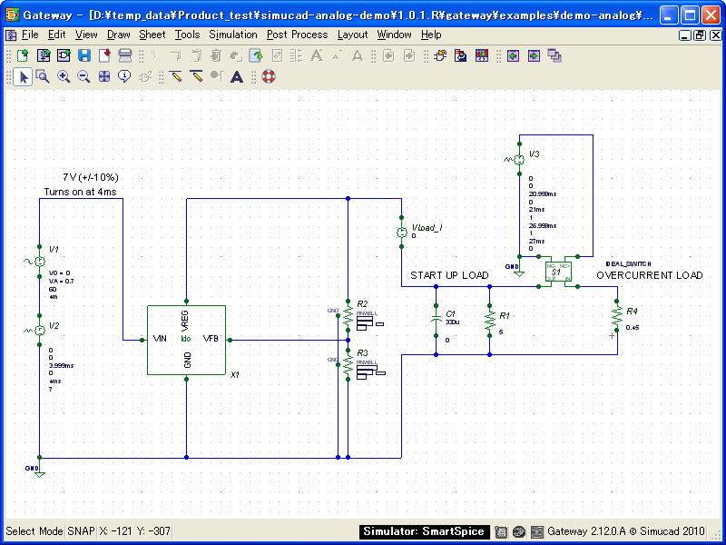
#1 : App_lvs1.net (Created from the schematic as shown in Figure 2
)
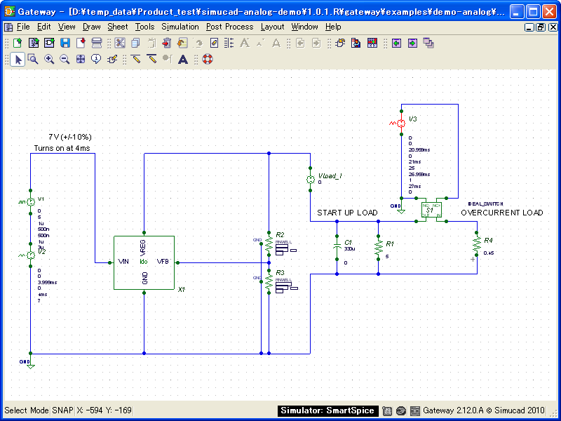
#2 : App_lvs2.net (Created from the schematic as shown in Figure 3
)
5) Click the OK button in the Project Settings dialog.
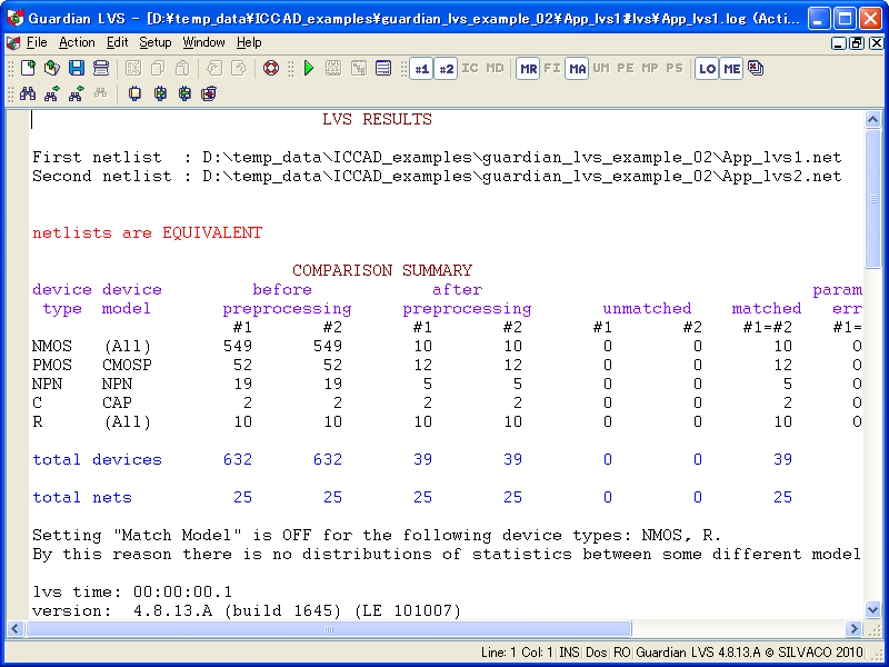
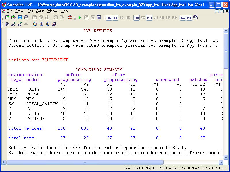
6) Select Action->Run Lvs from the Guardian LVS menu bar. The netlist comparison will be executed, and Guardian LVS will report that those netlist are EQUIVALENT (see Figure 4
).
In the log file, no specific SPICE elements such as V or SW will be reported, because they are ignored in the normal LVS process.
7) Select the Setup->Project Settings command again, and turn on the Process specific SPICE elements checkbox in the General page (see Figure 5
).
8) Run Lvs again.
Guardian LVS will still report that those netlist are EQUIVALENT , but the specific SPICE elements will be compared and reported in the log file (see Figure 6
).
9) Select the Setup->Project Settings command again, and open the Models page.
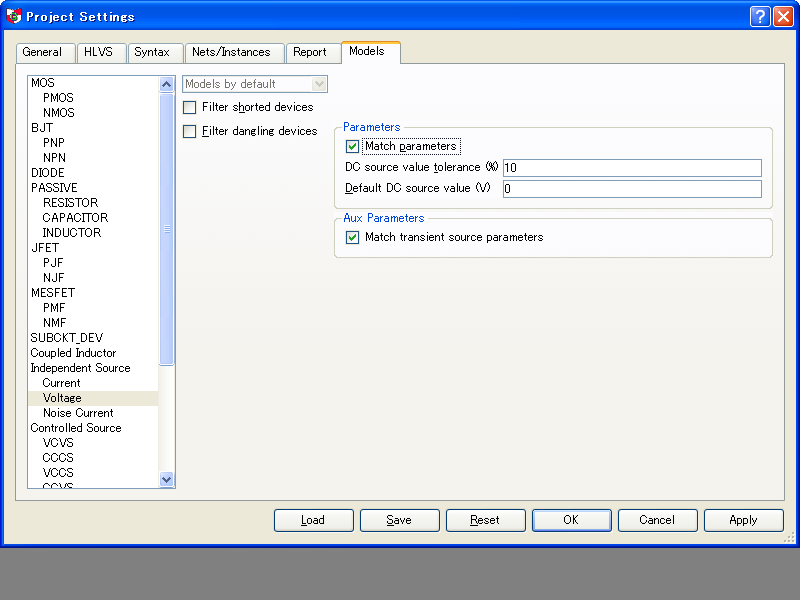
10) Select Independent Source->Voltage , and turn on the check boxes Match parameters and also Match transient source parameters (see Figure 7
).
11) Run Lvs again.
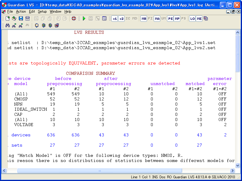
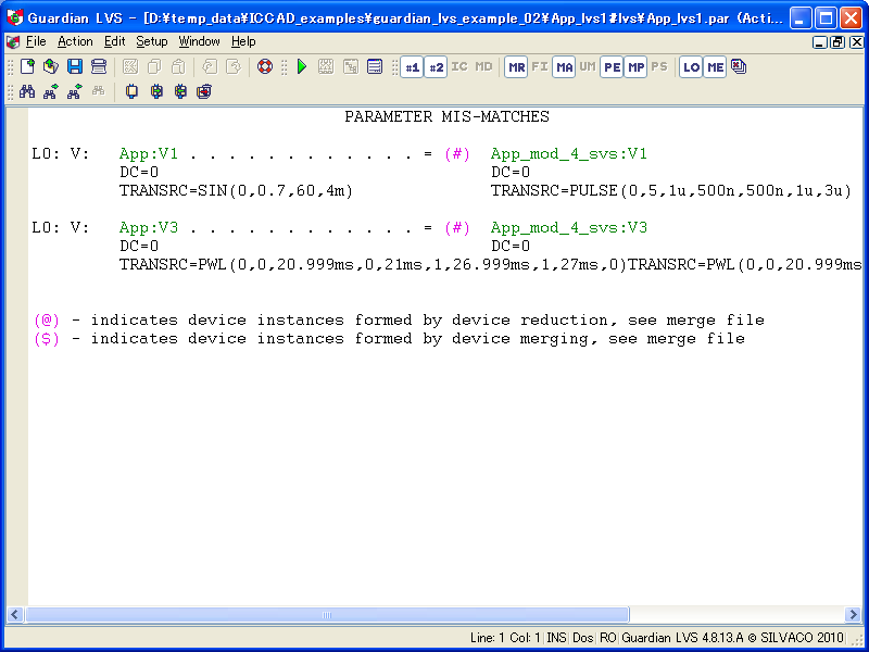
Guardian LVS will still report that those netlist are topologically EQUIVALENT , but some parameter errors are detected (see Figure 8
).
The details of discrepancies will be reported in the parameter error file (see Figure 9
).
Graphics
Input Files
App_lvs1.log
LVS RESULTS

First netlist  : D:\temp_data\ICCAD_examples\guardian_lvs_example_02\App_lvs1.net
Second netlist : D:\temp_data\ICCAD_examples\guardian_lvs_example_02\App_lvs2.net


netlists are topologically EQUIVALENT, parameter errors are detected

                          COMPARISON SUMMARY
device device         before            after                                 parameter
 type  model       preprocessing     preprocessing       unmatched    matched   error
                    #1       #2       #1       #2       #1       #2    #1=#2    #1=#2
NMOS   (All)       549      549       10       10        0        0       10      OFF
PMOS   CMOSP        52       52       12       12        0        0       12      OFF
NPN    NPN          19       19        5        5        0        0        5      OFF
SW     IDEAL_SWITCH  1        1        1        1        0        0        1      OFF
C      CAP           2        2        2        2        0        0        2      OFF
R      (All)        10       10       10       10        0        0       10      OFF
V      VOLTAGE       3        3        3        3        0        0        3        2

total devices      636      636       43       43        0        0       43        2

total nets          27       27       27       27        0        0       27

Setting "Match Model" is OFF for the following device types: NMOS, R.
By this reason there is no distributions of statistics between some different models for mentioned device types.

lvs time: 00:00:00.1
version:  4.8.13.R (build 1646) (LE 101014)
created:  Wed Oct 14 10:26:37 2010

                             LVS SETTINGS

Guardian message file           : D:\temp_data\ICCAD_examples\guardian_lvs_example_02\App_lvs1#lvs\App_lvs1.mes
Guardian filtered nodes file    : D:\temp_data\ICCAD_examples\guardian_lvs_example_02\App_lvs1#lvs\App_lvs1.flt
Guardian merged devices file    : D:\temp_data\ICCAD_examples\guardian_lvs_example_02\App_lvs1#lvs\App_lvs1.mrg
Guardian matched nodes file     : D:\temp_data\ICCAD_examples\guardian_lvs_example_02\App_lvs1#lvs\App_lvs1.mtc
Guardian unmatched nodes file   : D:\temp_data\ICCAD_examples\guardian_lvs_example_02\App_lvs1#lvs\App_lvs1.unm
Guardian parameter error file   : D:\temp_data\ICCAD_examples\guardian_lvs_example_02\App_lvs1#lvs\App_lvs1.par
Guardian parameter match file   : D:\temp_data\ICCAD_examples\guardian_lvs_example_02\App_lvs1#lvs\App_lvs1.pma
Guardian port swappability file : D:\temp_data\ICCAD_examples\guardian_lvs_example_02\App_lvs1#lvs\App_lvs1.psw

General Settings:

Use Local Matching on
Spreading Wave Algorithm on
Match same name nets off
Match same name devices/instances off
Match same name subcircuits off
Case-sensitive matching of names off
Simplified symmetry break off
Detect label mismatch off
Process specific SPICE elements on
Unmatched node limit: 100

HLVS Settings:

Hierarchical mode off
Equalize hierarchy of compared subcircuits on
Stop when first non-equivalent subcircuit pair is detected on
Combine high-shorted ports of subcircuits off
Detect floating ports of subcircuits off
Exclude parameterized subcircuits off
Resolve ambiguities for ports off
Use same port names off
Use swappability of port groups off

Syntax Settings:

Duplicated Subcircuit: ignore subcircuit
End-of-line comment characters: ;
Remove net name suffix starting from colon(:) off
Keep multiplier factor of devices off
Allow floating pins in subcircuit calls off
All subcircuit ports non-collapsible off
Collapsible nets: "All nets"

Report Settings:

Write match file on
Write merge file on
Write message file on
Write parameter match file on
Write filter file on
Write port swappability file on
Report LW parameters in microns on
Report guess statistics on
App_lvs1.net
* Gateway 2.12.0.A Guardian Netlist Generator
* Workspace name:       D:\temp_data\Product_test\simucad-analog-demo\1.0.1.R\gateway\SBCD_kuwa_2.work_space.workspace
* Simulation name:      D:\temp_data\Product_test\simucad-analog-demo\1.0.1.R\gateway\examples\demo-analog\App.schlr
* Simulation timestamp: 28-9-2010 15:46:56

* Schematic name: App
.SUBCKT App
C1 NET1 GND 330u IC=0
R1 NET1 GND 5
R_R2 NET3 VREG RNWELL L=9U W=0.3U M=1 $SUB=GND
R_R3 GND NET3 RNWELL L=36U W=0.3U M=1 $SUB=GND
R4 NET2 GND 0.45
S1 NET2 NET1 NET5 GND IDEAL_SWITCH /OFF
V1 Vps NET4 SIN(0 0.7 60 4m )
V2 NET4 GND PWL(0 0 3.999ms 0 4ms 7 )
V3 NET5 GND PWL(0 0 20.999ms 0 21ms 1 26.999ms 1 27ms 0 )
*THIS WAS A VOLTAGE SOURCE
X1 GND NET3 Vps VREG ldo
.ENDS App

* Schematic name: ldo
.SUBCKT ldo GND VFB VIN VREG
C1 NET5 GND 10p
M1 NET9 NET5 VREG VREG HVCMOSN L=2.5U W=100U M=500
R1 NET9 VIN 0.1
X1 GND VIN NET3 vref
X2 GND NET3 NET5 VFB VIN error_amp
.ENDS ldo

* Schematic name: vref
.SUBCKT vref GND VIN VOUT
M1 VOUT NET2 VIN VIN CMOSP L=25U W=100U M=1
M2 NET4 NET2 VIN VIN CMOSP L=25U W=100U M=1
M3 NET2 NET2 VIN VIN CMOSP L=25U W=100U M=1
M4 NET8 NET2 VIN VIN CMOSP L=25U W=100U M=1
Q1 VOUT VOUT NET1 GND NPN AREA=1 M=8
Q2 NET4 VOUT NET3 GND NPN AREA=1 M=1
Q3 NET8 NET8 GND GND NPN AREA=1 M=1
Q4 NET2 NET8 NET6 GND NPN AREA=1 M=8
R1 NET3 NET1 RPPLUS L=134.1U W=10u M=1 $SUB=VIN
R7 GND NET3 RPPLUS L=690.75U W=10U M=1 $SUB=VIN
R12 GND NET6 RPPLUS L=135.1U W=10U M=1 $SUB=VIN
.ENDS vref

* Schematic name: error_amp
.SUBCKT error_amp GND MINUS OUT PLUS VCC
M1 NET1 NET10 GND GND CMOSN L=2U W=5U M=1
M2 NET7 NET10 GND GND CMOSN L=2U W=5U M=1
M6 NET5 NET5 VCC VCC CMOSP L=2U W=10U M=1
M7 NET6 NET5 VCC VCC CMOSP L=2U W=10U M=1
M9 NET7 NET6 VCC VCC CMOSP L=2U W=10U M=1
M10 NET5 PLUS NET1 GND CMOSN L=2U W=5U M=1
M11 NET6 MINUS NET1 GND CMOSN L=2U W=5U M=1
M12 NET9 NET9 VCC VCC CMOSP L=2U W=10U M=1
M13 NET9 NET3 NET2 GND CMOSN L=2U W=5U M=1
M14 NET10 NET9 VCC VCC CMOSP L=2U W=10U M=1
M15 NET10 NET10 GND GND CMOSN L=2U W=5U M=1
M16 OUT NET12 VCC VCC CMOSP L=2U W=5U M=1
M17 NET12 NET7 VCC VCC CMOSP L=2U W=10U M=1
M18 NET12 NET7 GND GND CMOSN L=2U W=5U M=1
M19 NET12 NET12 VCC VCC CMOSP L=2U W=40U M=40
M20 OUT NET8 GND GND CMOSN L=2U W=5U M=1
M21 NET8 NET8 GND GND CMOSN L=2U W=5U M=40
M22 NET8 NET7 VCC VCC CMOSP L=2U W=10U M=1
M23 NET8 NET7 GND GND CMOSN L=2U W=5U M=1
Q1 NET3 NET2 GND GND NPN AREA=1 M=1
R2 GND NET2 RPPLUS L=34.5U W=0.3U M=1 $SUB=VCC
R_R1 NET3 VCC RNWELL L=9U W=0.3U M=1 $SUB=GND
.ENDS error_amp
*****model description
.model HVCMOSN NMOS
.model CMOSN NMOS
.model CMOSP PMOS
.model RPPLUS R
.model NPN NPN
.model IDEAL_SWITCH SW
******
*circuit netlist starts
******

* Global Nodes Declarations
.GLOBAL GND VDD

* End of the netlist
App_lvs2.net
* Gateway 2.12.0.A Guardian Netlist Generator
* Workspace name:       D:\temp_data\Product_test\simucad-analog-demo\1.0.1.R\gateway\SBCD_kuwa_2.work_space.workspace
* Simulation name:      D:\temp_data\Product_test\simucad-analog-demo\1.0.1.R\gateway\examples\demo-analog\App_mod_4_svs.schlr
* Simulation timestamp: 28-9-2010 15:57:03

* Schematic name: App_mod_4_svs
.SUBCKT App_mod_4_svs
C1 NET1 GND 330u IC=0
R1 NET1 GND 5
R_R2 NET3 VREG RNWELL L=9U W=0.3U M=1 $SUB=GND
R_R3 GND NET3 RNWELL L=36U W=0.3U M=1 $SUB=GND
R4 NET2 GND 0.45
S1 NET2 NET1 NET5 GND IDEAL_SWITCH /OFF
V1 Vps NET4 PULSE(0 5 1u 500n 500n 1u 3u)
V2 NET4 GND PWL(0 0 3.999ms 0 4ms 7 )
V3 NET5 GND PWL(0 0 20.999ms 0 21ms 25 26.999ms 1 27ms 0 )
*THIS WAS A VOLTAGE SOURCE
X1 GND NET3 Vps VREG ldo
.ENDS App_mod_4_svs

* Schematic name: ldo
.SUBCKT ldo GND VFB VIN VREG
C1 NET5 GND 10p
M1 NET9 NET5 VREG VREG HVCMOSN L=2.5U W=100U M=500
R1 NET9 VIN 0.1
X1 GND VIN NET3 vref
X2 GND NET3 NET5 VFB VIN error_amp
.ENDS ldo

* Schematic name: vref
.SUBCKT vref GND VIN VOUT
M1 VOUT NET2 VIN VIN CMOSP L=25U W=100U M=1
M2 NET4 NET2 VIN VIN CMOSP L=25U W=100U M=1
M3 NET2 NET2 VIN VIN CMOSP L=25U W=100U M=1
M4 NET8 NET2 VIN VIN CMOSP L=25U W=100U M=1
Q1 VOUT VOUT NET1 GND NPN AREA=1 M=8
Q2 NET4 VOUT NET3 GND NPN AREA=1 M=1
Q3 NET8 NET8 GND GND NPN AREA=1 M=1
Q4 NET2 NET8 NET6 GND NPN AREA=1 M=8
R1 NET3 NET1 RPPLUS L=134.1U W=10u M=1 $SUB=VIN
R7 GND NET3 RPPLUS L=690.75U W=10U M=1 $SUB=VIN
R12 GND NET6 RPPLUS L=135.1U W=10U M=1 $SUB=VIN
.ENDS vref

* Schematic name: error_amp
.SUBCKT error_amp GND MINUS OUT PLUS VCC
M1 NET1 NET10 GND GND CMOSN L=2U W=5U M=1
M2 NET7 NET10 GND GND CMOSN L=2U W=5U M=1
M6 NET5 NET5 VCC VCC CMOSP L=2U W=10U M=1
M7 NET6 NET5 VCC VCC CMOSP L=2U W=10U M=1
M9 NET7 NET6 VCC VCC CMOSP L=2U W=10U M=1
M10 NET5 PLUS NET1 GND CMOSN L=2U W=5U M=1
M11 NET6 MINUS NET1 GND CMOSN L=2U W=5U M=1
M12 NET9 NET9 VCC VCC CMOSP L=2U W=10U M=1
M13 NET9 NET3 NET2 GND CMOSN L=2U W=5U M=1
M14 NET10 NET9 VCC VCC CMOSP L=2U W=10U M=1
M15 NET10 NET10 GND GND CMOSN L=2U W=5U M=1
M16 OUT NET12 VCC VCC CMOSP L=2U W=5U M=1
M17 NET12 NET7 VCC VCC CMOSP L=2U W=10U M=1
M18 NET12 NET7 GND GND CMOSN L=2U W=5U M=1
M19 NET12 NET12 VCC VCC CMOSP L=2U W=40U M=40
M20 OUT NET8 GND GND CMOSN L=2U W=5U M=1
M21 NET8 NET8 GND GND CMOSN L=2U W=5U M=40
M22 NET8 NET7 VCC VCC CMOSP L=2U W=10U M=1
M23 NET8 NET7 GND GND CMOSN L=2U W=5U M=1
Q1 NET3 NET2 GND GND NPN AREA=1 M=1
R2 GND NET2 RPPLUS L=34.5U W=0.3U M=1 $SUB=VCC
R_R1 NET3 VCC RNWELL L=9U W=0.3U M=1 $SUB=GND
.ENDS error_amp
*****model description
.model HVCMOSN NMOS
.model CMOSN NMOS
.model CMOSP PMOS
.model RPPLUS R
.model NPN NPN
.model IDEAL_SWITCH SW
******
*circuit netlist starts
******

* Global Nodes Declarations
.GLOBAL GND VDD

* End of the netlist