

Minimum Required Versions: Expert 4.10.39.R & Gateway 2.12.32.R
Expert provides the capability of creating layout from a schematic netlist in Gateway. The netlist driven layout (NDL) flow is described in the following example using a D-Flip Flop circuit.
1.0. Preliminary steps to start example
- Add “Silvaco_demo_pcells” PCell library as a reference library by selecting Libraries->Setup , and clicking the “Add” icon and browsing to the file “Silvaco_demo_pcells.eld”
- Load the “expert_ex12.eld” project
1.1. Loading the Netlist
Select the menu item Tools->Netlist driven layout->Load netlist , and browse to the NDL netlist created in Gateway. This example uses the netlist dff_ndl.net. The PCell map file demo_pcells.map that links the netlist device names to the PCells will be loaded automatically because of it specified as Map file for NDL in technology data settings ( Setup->Technology->General ).
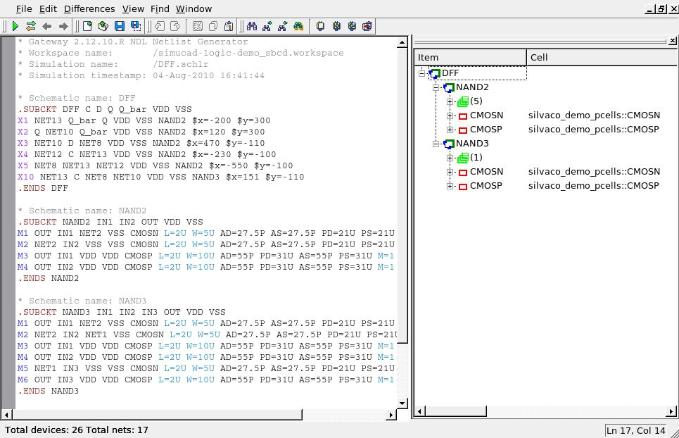
After the netlist is loaded, the Netlist Editor window will appear as shown in Figure 1
.
The left side of the window displays the netlist and the right side displays the Netlist Rover, which displays the circuit hierarchy and lists the netlist devices mapped to the corresponding PCells.
1.2. Creating the Layout
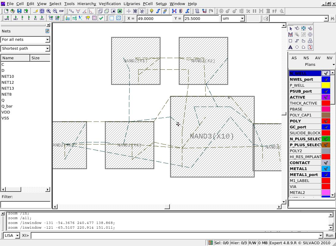
To create the layout, right click on the “DFF” topcell name in the Netlist Rover section of the Netlist Editor window and select “create”. All levels of hierarchy will be created containing the proper instances, and the top level cell will be opened in Expert and will appear as shown in Figure 2
.
The routing of the circuit can be done with the aid of the wire flight lines that you can see in cell. More info on the flight line guide can be found in the Wire flight lines guide Expert example in the Editing category.
1.3. Layout and Schematic Cross Probing
The Gateway schematic of the DFF and the Expert layout created through NDL can be linked so that cross probing of instances and nets can occur between the schematic and layout. Select the Expert menu item Verification->Launch Gateway , and a Gateway session will be opened in order to view the DFF schematic. Open the “expert_ex12.workspace” and open the DFF schematic located in ./symbols/logic/. Then select the Expert menu item Verification->Annotate .
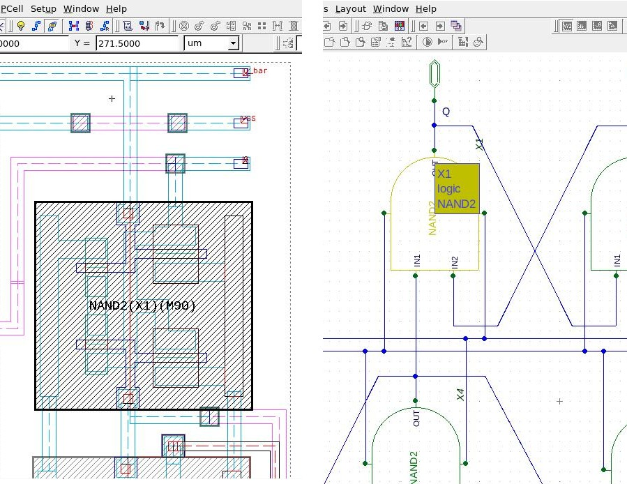
Now a layout instance in Expert can be selected and the corresponding schematic instance in Gateway will be highlighted. In Figure 3
the layout routing has been completed and the X1 NAND2 layout instance is selected in Expert on the left, and the same schematic instance highlighted in Gateway on the right.
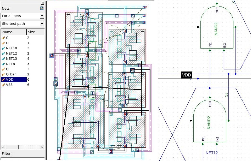
Circuit nodes can also be cross probed between layout and schematic. Figure 4
shows the VDD layout net selected and the VDD schematic net highlighted in Gateway.
Graphics
These examples are for reference only. Every software package contains a full set of examples suitable for that version and are installed with the software. If you see examples here that are not in your installation
you should consider updating to a later version of the software.
Input Files
demo_pcells.map
CMOSN silvaco_demo_pcells::CMOSN
CMOSP silvaco_demo_pcells::CMOSP
IND silvaco_demo_pcells::IND
NPN silvaco_demo_pcells::NPN
PIPCAP silvaco_demo_pcells::PIPCAP
RNPOLY silvaco_demo_pcells::RNPOLY
RNWELL silvaco_demo_pcells::RNWELL
RPOLY silvaco_demo_pcells::RPOLY
RPPLUS silvaco_demo_pcells::RPPLUS
dff_ndl.net
* Gateway 2.12.10.R NDL Netlist Generator
* Workspace name:       /simucad-logic-demo_sbcd.workspace
* Simulation name:      /DFF.schlr
* Simulation timestamp: 04-Aug-2010 16:41:44

* Schematic name: DFF
.SUBCKT DFF C D Q Q_bar VDD VSS
X1 NET13 Q_bar Q VDD VSS NAND2 $x=-200 $y=300
X2 Q NET10 Q_bar VDD VSS NAND2 $x=120 $y=300
X3 NET10 D NET8 VDD VSS NAND2 $x=470 $y=-110
X4 NET12 C NET13 VDD VSS NAND2 $x=-230 $y=-100
X5 NET8 NET13 NET12 VDD VSS NAND2 $x=-550 $y=-100
X10 NET13 C NET8 NET10 VDD VSS NAND3 $x=151 $y=-110
.ENDS DFF

* Schematic name: NAND2
.SUBCKT NAND2 IN1 IN2 OUT VDD VSS
M1 OUT IN1 NET2 VSS CMOSN L=2U W=5U AD=27.5P AS=27.5P PD=21U PS=21U M=1 $x=-149 $y=40
M2 NET2 IN2 VSS VSS CMOSN L=2U W=5U AD=27.5P AS=27.5P PD=21U PS=21U M=1 $x=-149 $y=-80
M3 OUT IN1 VDD VDD CMOSP L=2U W=10U AD=55P PD=31U AS=55P PS=31U M=1 $x=-199 $y=180
M4 OUT IN2 VDD VDD CMOSP L=2U W=10U AD=55P PD=31U AS=55P PS=31U M=1 $x=0 $y=180
.ENDS NAND2

* Schematic name: NAND3
.SUBCKT NAND3 IN1 IN2 IN3 OUT VDD VSS
M1 OUT IN1 NET2 VSS CMOSN L=2U W=5U AD=27.5P AS=27.5P PD=21U PS=21U M=1 $x=110 $y=300
M2 NET2 IN2 NET1 VSS CMOSN L=2U W=5U AD=27.5P AS=27.5P PD=21U PS=21U M=1 $x=110 $y=180
M3 OUT IN1 VDD VDD CMOSP L=2U W=10U AD=55P PD=31U AS=55P PS=31U M=1 $x=60 $y=440
M4 OUT IN2 VDD VDD CMOSP L=2U W=10U AD=55P PD=31U AS=55P PS=31U M=1 $x=260 $y=440
M5 NET1 IN3 VSS VSS CMOSN L=2U W=5U AD=27.5P AS=27.5P PD=21U PS=21U M=1 $x=110 $y=70
M6 OUT IN3 VDD VDD CMOSP L=2U W=10U AD=55P PD=31U AS=55P PS=31U M=1 $x=400 $y=440
.ENDS NAND3

* Global Nodes Declarations
.GLOBAL GND

* End of the netlist