

Requires: Utmost IV, SmartSpice, SmartView
Minimum Versions: Utmost IV 1.10.6.R, SmartSpice 4.10.2.R, SmartView 2.28.2.R
This example describes how to extract a resistor model including temperature
coefficients and delta geometry parameters.
The project file
opt_ex13.prj
and the data file
opt_ex13.uds
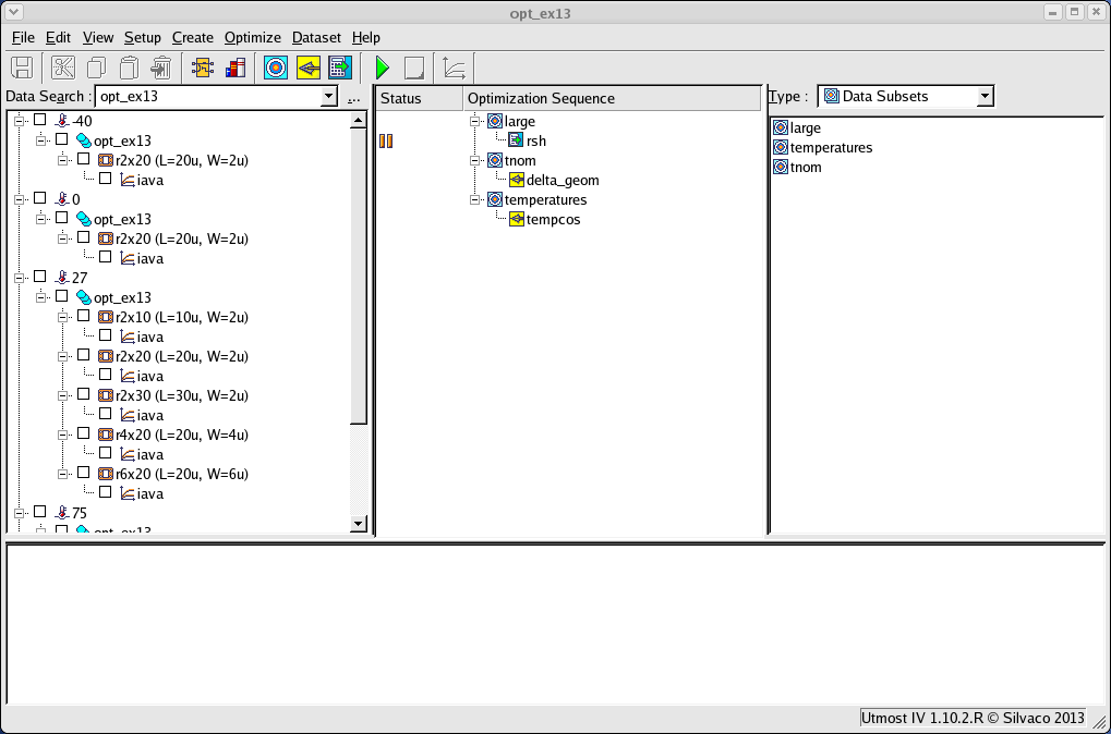
for this example should both be loaded into your database. When opened, the
project will look as shown in
opt_ex13_01.png
.
The optimization sequence, which fully automates the extraction of this
resistor model example, has three sections. The objective of each section
is to isolate a device characteristic and then to extract or optimize only
those model parameters which account for this device behavior.
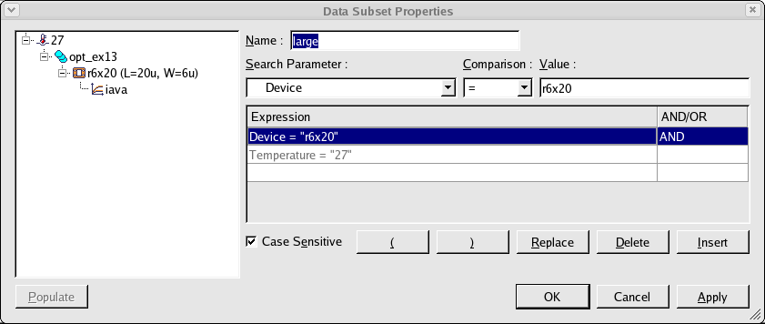
The first section, selects a single resistor measurement at the nominal temperature.
We chose the largest measured resistor to minimize the effects of delta width
and delta length as shown in
opt_ex13_02.png
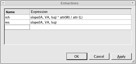
. From this single dataset, we can extract the sheet resistance
assuming that delta geometry effects are zero. This is done by the extraction
‘rsh’ which is defined as shown in
opt_ex13_03.png
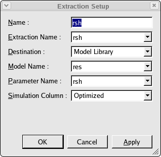
. The extraction setup, also called ‘rsh’, is used to select the extraction to
be performed on the single dataset and also defines where to write the result
as shown in
opt_ex13_04.png
. In this case, the extraction called ‘rsh’ is performed and the result is written
into the model parameter
RSH
of the model
RES
in the optimized column.
The second section deals with the delta geometry parameters. These are extracted
from all of the available resistor geometries measured at the nominal temperature.
The dataset subset definition is as shown in
opt_ex13_05.png
. In order to optimize the delta width parameter
DW
, you must have at least two resistors
with different widths. Likewise, you need at least two different lengths to extract the
delta length parameter
DLR
. In this example, there are resistors with three different widths
with the same length and three different lengths with the same width.
The previous section extracted a preliminary value for the
RSH
parameter assuming that the delta width and delta length are both zero. This section
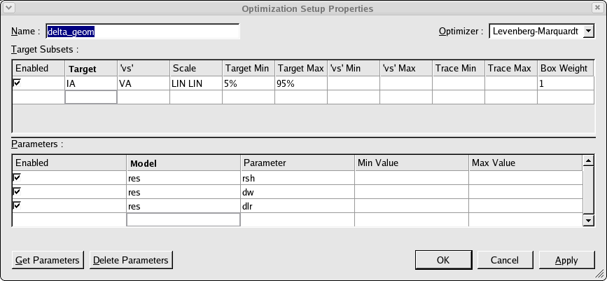
optimizes all three parameters
RSH, DW, DLR
as shown in
opt_ex13_06.png
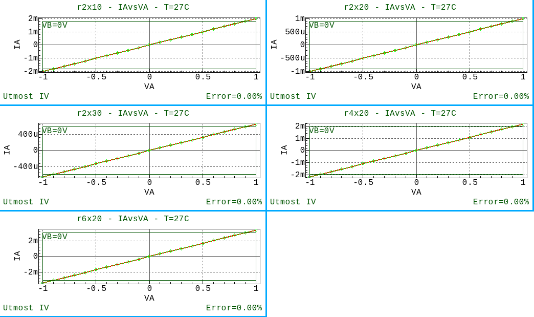
. Once the nominal temperature model has been extracted, the measured versus simulated
data will be displayed in the viewer as shown in
opt_ex13_07.png
.
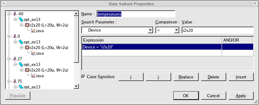
The final section deals with the temperature coefficients. One resistor has been measured
at five temperatures and the dataset subset definition is as shown in
opt_ex13_08.png
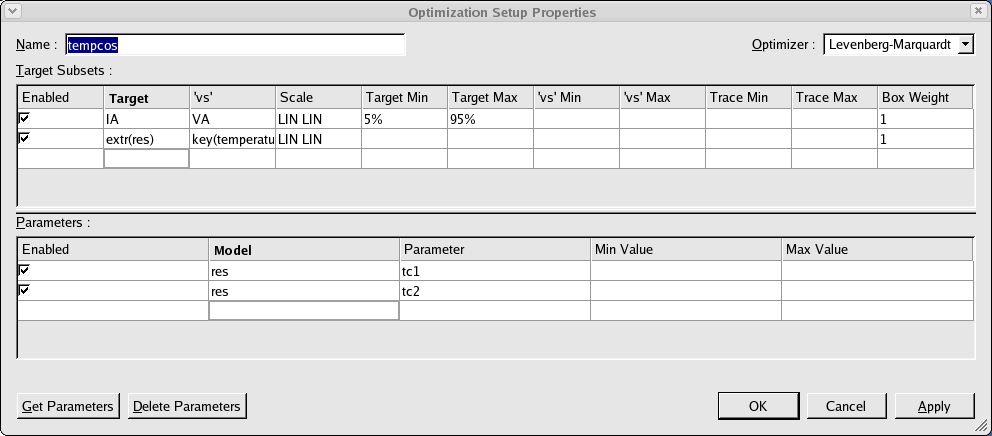
. In the optimization setup shown in
opt_ex13_09.png
, there are two targets defined. The first is the measured IV chacteristic for the resistors,
the second is a plot of extracted resistance value ‘res’ vs the temperature. Both of these
targets will be used during the optimization. The first and second order temperature
coefficients
TC1
and
TC2
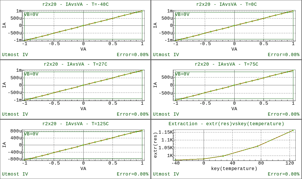
are optimized. Once this optimization has been run, the measured vs simulated IV and extracted
characteristics are displayed in the viewer as shown in
opt_ex13_10.png
.
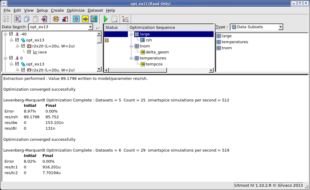
The results from the extraction and the optmizations are also shown in the project status log
area as shown in
opt_ex13_11.png
. The model card can then be exported into an external model library file as shown
in the output file
opt_ex13.lib.
Graphics

Files
opt_ex13.lib
.MODEL res R (
+tnom     = 27             rsh      = 85.752         dw       = 1.53101e-07
+dlr      = 1.31e-07       tc1      = 0.000916201    tc2      = 7.70194e-06 )
opt_ex13.uds
Utmost IV CSV Data Logfile
Format Version 1
Copyright (c) 1984-2016 Silvaco, Inc. All rights reserved


DataSetStart

DataSetName, res
MeasurementType, DC

BatchName, opt_ex13
WaferName, wafer1
DieName, x0y0
DeviceName, r2x20
Temperature, -40

FabDate, 18 Jan 2013
UserDate, 18 Jan 2013

WaferDiameter, 0.2
DieLayout, FOUR_CROSSING
DieSize, 0.02, 0.02

Attribute, L, 2e-05
Attribute, W, 2e-06

NodeNames, a b

Sweep, 1, V, A, LIN, -1, 1, 0.1, CALCULATED, 0.1, 0

Constant, V, B, 0, 0.1, 0

Target, I, A

Plot, iava, XY (LIN LIN), VA, IA

DataArray, IA
-0.00102829    -0.000925465   -0.000822636   -0.000719806   -0.000616977
-0.000514147   -0.000411318   -0.000308488   -0.000205659   -0.000102829
0              0.000102829    0.000205659    0.000308488    0.000411318
0.000514147    0.000616977    0.000719806    0.000822636    0.000925465
0.00102829

DataSetFinish

DataSetStart

DataSetName, res
MeasurementType, DC

BatchName, opt_ex13
WaferName, wafer1
DieName, x0y0
DeviceName, r2x20
Temperature, 0

FabDate, 18 Jan 2013
UserDate, 18 Jan 2013

WaferDiameter, 0.2
DieLayout, FOUR_CROSSING
DieSize, 0.02, 0.02

Attribute, L, 2e-05
Attribute, W, 2e-06

NodeNames, a b

Sweep, 1, V, A, LIN, -1, 1, 0.1, CALCULATED, 0.1, 0

Constant, V, B, 0, 0.1, 0

Target, I, A

Plot, iava, XY (LIN LIN), VA, IA

DataArray, IA
-0.00102023    -0.000918211   -0.000816188   -0.000714164   -0.000612141
-0.000510117   -0.000408094   -0.00030607    -0.000204047   -0.000102023
0              0.000102023    0.000204047    0.00030607     0.000408094
0.000510117    0.000612141    0.000714164    0.000816188    0.000918211
0.00102023

DataSetFinish

DataSetStart

DataSetName, res
MeasurementType, DC

BatchName, opt_ex13
WaferName, wafer1
DieName, x0y0
DeviceName, r2x10
Temperature, 27

FabDate, 18 Jan 2013
UserDate, 18 Jan 2013

WaferDiameter, 0.2
DieLayout, FOUR_CROSSING
DieSize, 0.02, 0.02

Attribute, L, 1e-05
Attribute, W, 2e-06

NodeNames, a b

Sweep, 1, V, A, LIN, -1, 1, 0.1, CALCULATED, 0.1, 0

Constant, V, B, 0, 0.1, 0

Target, I, A

Plot, iava, XY (LIN LIN), VA, IA

DataArray, IA
-0.00202837    -0.00182554    -0.0016227     -0.00141986    -0.00121702
-0.00101419    -0.00081135    -0.000608512   -0.000405675   -0.000202837
0              0.000202837    0.000405675    0.000608512    0.00081135
0.00101419     0.00121702     0.00141986     0.0016227      0.00182554
0.00202837

DataSetFinish

DataSetStart

DataSetName, res
MeasurementType, DC

BatchName, opt_ex13
WaferName, wafer1
DieName, x0y0
DeviceName, r2x20
Temperature, 27

FabDate, 18 Jan 2013
UserDate, 18 Jan 2013

WaferDiameter, 0.2
DieLayout, FOUR_CROSSING
DieSize, 0.02, 0.02

Attribute, L, 2e-05
Attribute, W, 2e-06

NodeNames, a b

Sweep, 1, V, A, LIN, -1, 1, 0.1, CALCULATED, 0.1, 0

Constant, V, B, 0, 0.1, 0

Target, I, A

Plot, iava, XY (LIN LIN), VA, IA

DataArray, IA
-0.00100072    -0.000900652   -0.00080058    -0.000700507   -0.000600435
-0.000500362   -0.00040029    -0.000300217   -0.000200145   -0.000100072
0              0.000100072    0.000200145    0.000300217    0.00040029
0.000500362    0.000600435    0.000700507    0.00080058     0.000900652
0.00100072

DataSetFinish

DataSetStart

DataSetName, res
MeasurementType, DC

BatchName, opt_ex13
WaferName, wafer1
DieName, x0y0
DeviceName, r2x30
Temperature, 27

FabDate, 18 Jan 2013
UserDate, 18 Jan 2013

WaferDiameter, 0.2
DieLayout, FOUR_CROSSING
DieSize, 0.02, 0.02

Attribute, L, 3e-05
Attribute, W, 2e-06

NodeNames, a b

Sweep, 1, V, A, LIN, -1, 1, 0.1, CALCULATED, 0.1, 0

Constant, V, B, 0, 0.1, 0

Target, I, A

Plot, iava, XY (LIN LIN), VA, IA

DataArray, IA
-0.000664211   -0.00059779    -0.000531369   -0.000464948   -0.000398527
-0.000332106   -0.000265684   -0.000199263   -0.000132842   -6.64211e-05
0              6.64211e-05    0.000132842    0.000199263    0.000265684
0.000332106    0.000398527    0.000464948    0.000531369    0.00059779
0.000664211

DataSetFinish

DataSetStart

DataSetName, res
MeasurementType, DC

BatchName, opt_ex13
WaferName, wafer1
DieName, x0y0
DeviceName, r4x20
Temperature, 27

FabDate, 18 Jan 2013
UserDate, 18 Jan 2013

WaferDiameter, 0.2
DieLayout, FOUR_CROSSING
DieSize, 0.02, 0.02

Attribute, L, 2e-05
Attribute, W, 4e-06

NodeNames, a b

Sweep, 1, V, A, LIN, -1, 1, 0.1, CALCULATED, 0.1, 0

Constant, V, B, 0, 0.1, 0

Target, I, A

Plot, iava, XY (LIN LIN), VA, IA

DataArray, IA
-0.00218236    -0.00196412    -0.00174589    -0.00152765    -0.00130941
-0.00109118    -0.000872943   -0.000654707   -0.000436472   -0.000218236
0              0.000218236    0.000436472    0.000654707    0.000872943
0.00109118     0.00130941     0.00152765     0.00174589     0.00196412
0.00218236

DataSetFinish

DataSetStart

DataSetName, res
MeasurementType, DC

BatchName, opt_ex13
WaferName, wafer1
DieName, x0y0
DeviceName, r6x20
Temperature, 27

FabDate, 18 Jan 2013
UserDate, 18 Jan 2013

WaferDiameter, 0.2
DieLayout, FOUR_CROSSING
DieSize, 0.02, 0.02

Attribute, L, 2e-05
Attribute, W, 6e-06

NodeNames, a b

Sweep, 1, V, A, LIN, -1, 1, 0.1, CALCULATED, 0.1, 0

Constant, V, B, 0, 0.1, 0

Target, I, A

Plot, iava, XY (LIN LIN), VA, IA

DataArray, IA
-0.00336399    -0.00302759    -0.00269119    -0.00235479    -0.00201839
-0.001682      -0.0013456     -0.0010092     -0.000672798   -0.000336399
0              0.000336399    0.000672798    0.0010092      0.0013456
0.001682       0.00201839     0.00235479     0.00269119     0.00302759
0.00336399

DataSetFinish

DataSetStart

DataSetName, res
MeasurementType, DC

BatchName, opt_ex13
WaferName, wafer1
DieName, x0y0
DeviceName, r2x20
Temperature, 75

FabDate, 18 Jan 2013
UserDate, 18 Jan 2013

WaferDiameter, 0.2
DieLayout, FOUR_CROSSING
DieSize, 0.02, 0.02

Attribute, L, 2e-05
Attribute, W, 2e-06

NodeNames, a b

Sweep, 1, V, A, LIN, -1, 1, 0.1, CALCULATED, 0.1, 0

Constant, V, B, 0, 0.1, 0

Target, I, A

Plot, iava, XY (LIN LIN), VA, IA

DataArray, IA
-0.000942548   -0.000848293   -0.000754038   -0.000659784   -0.000565529
-0.000471274   -0.000377019   -0.000282764   -0.00018851    -9.42548e-05
0              9.42548e-05    0.00018851     0.000282764    0.000377019
0.000471274    0.000565529    0.000659784    0.000754038    0.000848293
0.000942548

DataSetFinish

DataSetStart

DataSetName, res
MeasurementType, DC

BatchName, opt_ex13
WaferName, wafer1
DieName, x0y0
DeviceName, r2x20
Temperature, 125

FabDate, 18 Jan 2013
UserDate, 18 Jan 2013

WaferDiameter, 0.2
DieLayout, FOUR_CROSSING
DieSize, 0.02, 0.02

Attribute, L, 2e-05
Attribute, W, 2e-06

NodeNames, a b

Sweep, 1, V, A, LIN, -1, 1, 0.1, CALCULATED, 0.1, 0

Constant, V, B, 0, 0.1, 0

Target, I, A

Plot, iava, XY (LIN LIN), VA, IA

DataArray, IA
-0.000859908   -0.000773917   -0.000687927   -0.000601936   -0.000515945
-0.000429954   -0.000343963   -0.000257972   -0.000171982   -8.59908e-05
0              8.59908e-05    0.000171982    0.000257972    0.000343963
0.000429954    0.000515945    0.000601936    0.000687927    0.000773917
0.000859908

DataSetFinish