 https://silvaco.com/wp-content/uploads/2019/07/VT_fig2.jpg
283
401
Erick Castellon
/wp-content/uploads/2019/11/silvaco-logo.png
Erick Castellon2019-07-05 00:00:502020-12-22 10:31:30TCAD Simulation of Electric Field Distribution in Gallium Nitride Trench-based Power Devices
https://silvaco.com/wp-content/uploads/2019/07/VT_fig2.jpg
283
401
Erick Castellon
/wp-content/uploads/2019/11/silvaco-logo.png
Erick Castellon2019-07-05 00:00:502020-12-22 10:31:30TCAD Simulation of Electric Field Distribution in Gallium Nitride Trench-based Power Devices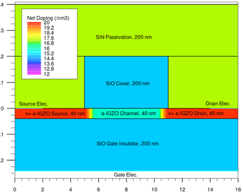 https://silvaco.com/wp-content/uploads/2020/02/ss_self-heating_fig1.jpg
397
550
Erick Castellon
/wp-content/uploads/2019/11/silvaco-logo.png
Erick Castellon2019-07-04 00:00:192020-12-21 12:09:58Channel-length Dependence of a-IGZO TFTs with Self-heating Effects
https://silvaco.com/wp-content/uploads/2020/02/ss_self-heating_fig1.jpg
397
550
Erick Castellon
/wp-content/uploads/2019/11/silvaco-logo.png
Erick Castellon2019-07-04 00:00:192020-12-21 12:09:58Channel-length Dependence of a-IGZO TFTs with Self-heating Effects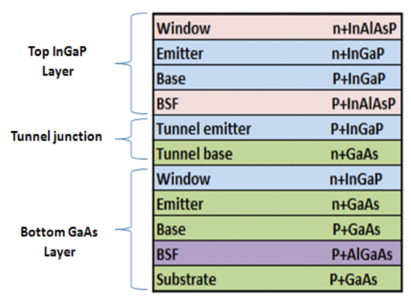 https://silvaco.com/wp-content/uploads/2020/02/solar_cell_fig2.jpg
299
411
Erick Castellon
/wp-content/uploads/2019/11/silvaco-logo.png
Erick Castellon2019-07-03 00:00:592020-12-22 11:14:21Simulation of Different Tunnel Junctions in InGaP/GaAs, InGaP/CdTe Dual Junction Solar Cells
https://silvaco.com/wp-content/uploads/2020/02/solar_cell_fig2.jpg
299
411
Erick Castellon
/wp-content/uploads/2019/11/silvaco-logo.png
Erick Castellon2019-07-03 00:00:592020-12-22 11:14:21Simulation of Different Tunnel Junctions in InGaP/GaAs, InGaP/CdTe Dual Junction Solar Cells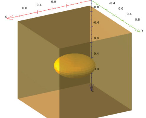 https://silvaco.com/wp-content/uploads/2019/07/hts-July-2019-thumb.png
875
900
Erick Castellon
/wp-content/uploads/2019/11/silvaco-logo.png
Erick Castellon2019-07-01 22:50:502020-12-19 12:18:06Hints, Tips and Solutions – July, August, September 2019
https://silvaco.com/wp-content/uploads/2019/07/hts-July-2019-thumb.png
875
900
Erick Castellon
/wp-content/uploads/2019/11/silvaco-logo.png
Erick Castellon2019-07-01 22:50:502020-12-19 12:18:06Hints, Tips and Solutions – July, August, September 2019 https://silvaco.com/wp-content/uploads/2019/04/VP_fig5.jpg
471
550
Erick Castellon
/wp-content/uploads/2019/11/silvaco-logo.png
Erick Castellon2019-04-01 10:00:342020-12-22 12:20:23Process Simulation – New Features in 2019 Baseline Release
https://silvaco.com/wp-content/uploads/2019/04/VP_fig5.jpg
471
550
Erick Castellon
/wp-content/uploads/2019/11/silvaco-logo.png
Erick Castellon2019-04-01 10:00:342020-12-22 12:20:23Process Simulation – New Features in 2019 Baseline Release https://silvaco.com/wp-content/uploads/2020/03/fig11.jpg
469
550
Erick Castellon
/wp-content/uploads/2019/11/silvaco-logo.png
Erick Castellon2019-04-01 09:00:112020-12-22 13:08:38Meshing – New Features in 2019 Baseline Release
https://silvaco.com/wp-content/uploads/2020/03/fig11.jpg
469
550
Erick Castellon
/wp-content/uploads/2019/11/silvaco-logo.png
Erick Castellon2019-04-01 09:00:112020-12-22 13:08:38Meshing – New Features in 2019 Baseline Release https://silvaco.com/wp-content/uploads/2019/04/device_fig2-6b.jpg
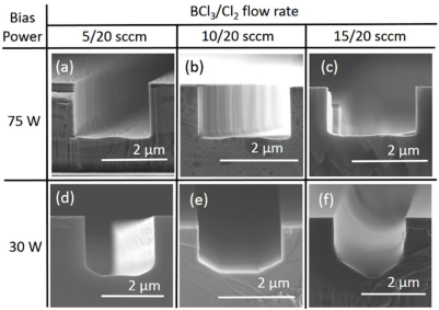
312
312
Erick Castellon
/wp-content/uploads/2019/11/silvaco-logo.png
Erick Castellon2019-04-01 08:00:192020-12-21 12:59:29Device Simulation – New Features in 2019 Baseline Release
https://silvaco.com/wp-content/uploads/2019/04/device_fig2-6b.jpg
312
312
Erick Castellon
/wp-content/uploads/2019/11/silvaco-logo.png
Erick Castellon2019-04-01 08:00:192020-12-21 12:59:29Device Simulation – New Features in 2019 Baseline Release https://silvaco.com/wp-content/uploads/2020/03/DB_fig4-6.jpg
425
550
Erick Castellon
/wp-content/uploads/2019/11/silvaco-logo.png
Erick Castellon2019-04-01 07:00:592020-12-22 16:40:09Interactive Tools – New Features in 2019 Baseline Release
https://silvaco.com/wp-content/uploads/2020/03/DB_fig4-6.jpg
425
550
Erick Castellon
/wp-content/uploads/2019/11/silvaco-logo.png
Erick Castellon2019-04-01 07:00:592020-12-22 16:40:09Interactive Tools – New Features in 2019 Baseline Release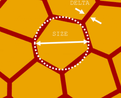 https://silvaco.com/wp-content/uploads/2020/03/3D_TFT_fig1.jpg
554
550
Erick Castellon
/wp-content/uploads/2019/11/silvaco-logo.png
Erick Castellon2019-01-01 10:00:392020-12-20 16:22:593D TFT Simulation of Grains and Grain Boundaries
https://silvaco.com/wp-content/uploads/2020/03/3D_TFT_fig1.jpg
554
550
Erick Castellon
/wp-content/uploads/2019/11/silvaco-logo.png
Erick Castellon2019-01-01 10:00:392020-12-20 16:22:593D TFT Simulation of Grains and Grain Boundaries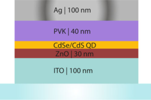 https://silvaco.com/wp-content/uploads/2020/03/hyLED__fig1a.jpg
329
550
Erick Castellon
/wp-content/uploads/2019/11/silvaco-logo.png
Erick Castellon2019-01-01 08:00:442020-12-22 12:19:22Quantum Dot-Based Hybrid Light Emitting Diode Modelling Using Radiant
https://silvaco.com/wp-content/uploads/2020/03/hyLED__fig1a.jpg
329
550
Erick Castellon
/wp-content/uploads/2019/11/silvaco-logo.png
Erick Castellon2019-01-01 08:00:442020-12-22 12:19:22Quantum Dot-Based Hybrid Light Emitting Diode Modelling Using Radiant