Semiconductor Process and Device Simulation
TCAD software solutions are key to developing new semiconductor processes and devices, dramatically reducing costs and time to market.
Implantation
Diffusion
Oxidation
Etch, Deposition, Epitaxy
Photolithography
Stress
- 2D and 3D Device Re-Meshing
- 2D and 3D Solid Modeling
Drift-Diffusion Based Device Physics
DC, AC, and Transient Analysis
Mixed Mode Simulation (TCAD + SPICE co-simulation)
Optical + Electrical Simulation
Atomic-Scale Transport Simulation
Device Characterization and SPICE Modeling
RC Extraction
High Performance and High Accuracy Parallel SPICE Simulator
Design Of Experiments
Interactive Tools
Machine Learning-based Analytics
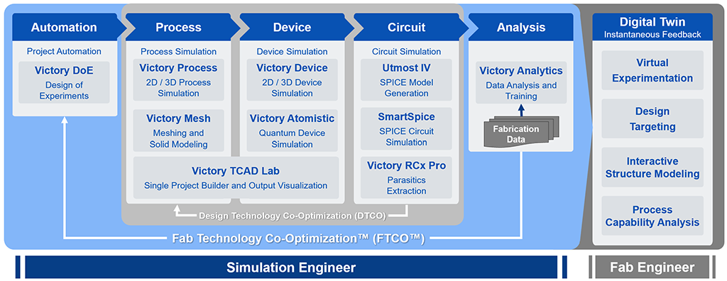
FTCO
Visualize Internal Physical Processes
- Using simulation, you can see ‘inside” the device. Experimental measurements tell you what happens, but not why it happens. TCAD can tell you why. For example:
- Reverse voltage characterization on a power device tells you what happens at high reverse biases. The device experiences reverse breakdown at a specific voltage
- A TCAD simulation can also replicate the reverse current-voltage curve, but also can also tell you why the device is experiencing breakdown. In TCAD the engineer can “see inside” the device and identify what region within the semiconductor first succumbs to breakdown due to high impact ionization generation
Fab Technology Co-Optimization™ (FTCO™)
Silvaco’s FTCO™ solution leverages artificial intelligence (AI) and machine learning (ML), as well as Physical Simulation in concert with Experimental Data, to generate a Digital Twin which is a digital counterpart that mirrors the form, fit and function of the physical world.
FTCO enables optimization of manufacturing processes, reduced costs, increased yields and ultimately leads to higher-quality semiconductor devices and improved manufacturing productivity.
Design Technology Co-Optimization (DTCO)
- TCAD is part of a DTCO flow which improves designs across multiple domains – Layout, Process, Device, SPICE, and RC extraction
- A full TCAD to SPICE flow, in an integrated DTCO environment, delivers clear actionable results for circuit design optimization
Virtual Experimentation
- Experiment with cause and effect: Change the device design (layout), technology (semiconductor process steps) or device operation condition (biasing, etc.), and understand and improve device performance
- Experiment with theories in TCAD: control the impact of various physics in the device via model settings and coefficients. If theory as applied to simulation matches the measured result, you may have found the root cause and gained physical understanding of device performance
Communicate Device Complexities Clearly
- Semiconductor device design, and processing of semiconductors is a complex task. Engineers must work collaboratively to solve problems, explain issues and opportunities to a variety of colleagues with varied technical expertise
- Utilizing TCAD can clearly communicate device and process changes; communicating potential performance improvements with clarity while minimizing manufacturing cycle times
Silvaco TCAD solutions are built in-house and are industry proven with thousands of Commercial, Government, and University customers and decades of proven use in the semiconductor industry !


Accelerating Next-Generation Power Technologies with AI-Powered FTCO
Organic Transport Model for Tandem Organic Light-Emitting Diode
Enabling the Next Generation of High-Voltage Power: Gallium Oxide Trench Schottky Diodes from Simulation to System
Victory TCAD 2025 Release