 https://silvaco.com/wp-content/uploads/2020/03/simstd_Q4_2013_a2.jpg
1012
782
Ingrid Schwarz
/wp-content/uploads/2019/11/silvaco-logo.png
Ingrid Schwarz2013-10-01 15:24:112020-12-20 15:56:18Atlas Simulation of a Wide Bandgap Gallium Oxide (Ga2O3) MOSFET
https://silvaco.com/wp-content/uploads/2020/03/simstd_Q4_2013_a2.jpg
1012
782
Ingrid Schwarz
/wp-content/uploads/2019/11/silvaco-logo.png
Ingrid Schwarz2013-10-01 15:24:112020-12-20 15:56:18Atlas Simulation of a Wide Bandgap Gallium Oxide (Ga2O3) MOSFET https://silvaco.com/wp-content/uploads/2020/03/simstd_Q4_2013_a1.jpg
1012
782
Ingrid Schwarz
/wp-content/uploads/2019/11/silvaco-logo.png
Ingrid Schwarz2013-10-01 15:18:062020-12-22 11:21:49Simulation of a DBR Edge Emitting Laser with External Air Gap Tuning Mirror
https://silvaco.com/wp-content/uploads/2020/03/simstd_Q4_2013_a1.jpg
1012
782
Ingrid Schwarz
/wp-content/uploads/2019/11/silvaco-logo.png
Ingrid Schwarz2013-10-01 15:18:062020-12-22 11:21:49Simulation of a DBR Edge Emitting Laser with External Air Gap Tuning Mirror https://silvaco.com/wp-content/uploads/2020/03/simstd_Q3_2013_a3.jpg
1012
782
Ingrid Schwarz
/wp-content/uploads/2019/11/silvaco-logo.png
Ingrid Schwarz2013-07-01 15:43:342020-12-20 16:52:50Anode Shorts Layout Dependence of Bi-mode IGBT (BiGT) On-state Characteristics
https://silvaco.com/wp-content/uploads/2020/03/simstd_Q3_2013_a3.jpg
1012
782
Ingrid Schwarz
/wp-content/uploads/2019/11/silvaco-logo.png
Ingrid Schwarz2013-07-01 15:43:342020-12-20 16:52:50Anode Shorts Layout Dependence of Bi-mode IGBT (BiGT) On-state Characteristics https://silvaco.com/wp-content/uploads/2020/03/simstd_Q3_2013_hints.jpg
1012
782
Ingrid Schwarz
/wp-content/uploads/2019/11/silvaco-logo.png
Ingrid Schwarz2013-07-01 15:38:402021-01-22 14:08:53Hints, Tips and Solutions – Compare the Results of Breakdown Simulations with Hatakeyama’s Impact Ionization Model for 4H-SiC Based Power Devices
https://silvaco.com/wp-content/uploads/2020/03/simstd_Q3_2013_hints.jpg
1012
782
Ingrid Schwarz
/wp-content/uploads/2019/11/silvaco-logo.png
Ingrid Schwarz2013-07-01 15:38:402021-01-22 14:08:53Hints, Tips and Solutions – Compare the Results of Breakdown Simulations with Hatakeyama’s Impact Ionization Model for 4H-SiC Based Power Devices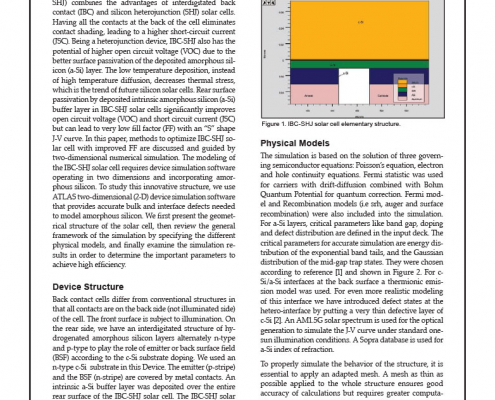 https://silvaco.com/wp-content/uploads/2020/03/simstd_Q3_2013_a2.jpg
1012
782
Ingrid Schwarz
/wp-content/uploads/2019/11/silvaco-logo.png
Ingrid Schwarz2013-07-01 15:16:312020-12-20 16:12:182D IBC-SHJ Solar Cell Simulation and Optimization
https://silvaco.com/wp-content/uploads/2020/03/simstd_Q3_2013_a2.jpg
1012
782
Ingrid Schwarz
/wp-content/uploads/2019/11/silvaco-logo.png
Ingrid Schwarz2013-07-01 15:16:312020-12-20 16:12:182D IBC-SHJ Solar Cell Simulation and Optimization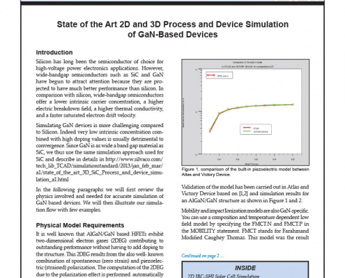 https://silvaco.com/wp-content/uploads/2020/03/simstd_Q3_2013_a1.jpg
1012
782
Ingrid Schwarz
/wp-content/uploads/2019/11/silvaco-logo.png
Ingrid Schwarz2013-07-01 15:12:322020-12-22 10:38:01State of the Art 2D and 3D Process and Device Simulation of GaN-Based Devices
https://silvaco.com/wp-content/uploads/2020/03/simstd_Q3_2013_a1.jpg
1012
782
Ingrid Schwarz
/wp-content/uploads/2019/11/silvaco-logo.png
Ingrid Schwarz2013-07-01 15:12:322020-12-22 10:38:01State of the Art 2D and 3D Process and Device Simulation of GaN-Based Devices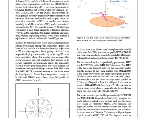 https://silvaco.com/wp-content/uploads/2020/03/simstd_Q2_2013_hints.jpg
1012
782
Ingrid Schwarz
/wp-content/uploads/2019/11/silvaco-logo.png
Ingrid Schwarz2013-04-01 14:49:132020-12-22 16:47:27Hints, Tips and Solutions – Setup Athena Monte Carlo Simulation of Ion Implantation in Silicon Carbide
https://silvaco.com/wp-content/uploads/2020/03/simstd_Q2_2013_hints.jpg
1012
782
Ingrid Schwarz
/wp-content/uploads/2019/11/silvaco-logo.png
Ingrid Schwarz2013-04-01 14:49:132020-12-22 16:47:27Hints, Tips and Solutions – Setup Athena Monte Carlo Simulation of Ion Implantation in Silicon Carbide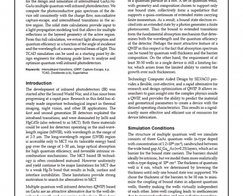 https://silvaco.com/wp-content/uploads/2020/03/simstd_Q2_2013_a3.jpg
1012
782
Ingrid Schwarz
/wp-content/uploads/2019/11/silvaco-logo.png
Ingrid Schwarz2013-04-01 14:45:522020-12-22 10:28:32TCAD Simulation of Multiple Quantum Well Infrared Photodetector (QWIP)
https://silvaco.com/wp-content/uploads/2020/03/simstd_Q2_2013_a3.jpg
1012
782
Ingrid Schwarz
/wp-content/uploads/2019/11/silvaco-logo.png
Ingrid Schwarz2013-04-01 14:45:522020-12-22 10:28:32TCAD Simulation of Multiple Quantum Well Infrared Photodetector (QWIP)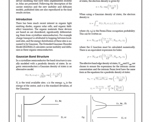 https://silvaco.com/wp-content/uploads/2020/03/simstd_Q2_2013_a2.jpg
1012
782
Ingrid Schwarz
/wp-content/uploads/2019/11/silvaco-logo.png
Ingrid Schwarz2013-04-01 14:42:052020-12-22 10:17:28The Extended Gaussian Disorder Model in Atlas
https://silvaco.com/wp-content/uploads/2020/03/simstd_Q2_2013_a2.jpg
1012
782
Ingrid Schwarz
/wp-content/uploads/2019/11/silvaco-logo.png
Ingrid Schwarz2013-04-01 14:42:052020-12-22 10:17:28The Extended Gaussian Disorder Model in Atlas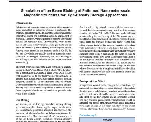 https://silvaco.com/wp-content/uploads/2020/03/simstd_Q2_2013_a1.jpg
1012
782
Ingrid Schwarz
/wp-content/uploads/2019/11/silvaco-logo.png
Ingrid Schwarz2013-04-01 14:36:562020-12-22 11:13:36Simulation of Ion Beam Etching of Patterned Nanometer-scale Magnetic Structures for High-Density Storage Applications
https://silvaco.com/wp-content/uploads/2020/03/simstd_Q2_2013_a1.jpg
1012
782
Ingrid Schwarz
/wp-content/uploads/2019/11/silvaco-logo.png
Ingrid Schwarz2013-04-01 14:36:562020-12-22 11:13:36Simulation of Ion Beam Etching of Patterned Nanometer-scale Magnetic Structures for High-Density Storage Applications