011_hierarchical : Inverter-equivalent Design (4-Bit Carry Look Ahead Adder)
Requires: SmartSpice & Smartview
Minimum Versions: SmartSpice 4.18.16.R and SmartView 2.32.5.R
This hierarchical design example demonstrates inverter-equivalent implementation of complex gates connected as a 4-Bit Carry Look Ahead (CLA) Adder circuit . The 4-Bit CLA Adder is implemented with dynamic logic using a Manchester Carry Chain (MCC) architecture.
One approach to designing complex digital circuits matches complex gate performance to a base inverter. The approach defines NMOS and PMOS transistor W/L ratios in complex gates according to those established in the base inverter. In some cases, such as those found in the MCC subcircuit, the base inverter-equivalent ratios must be scaled in complex ways to achieve the essential requirements.
In the schematics and circuits that follow, notice the use of global width (W) and length (L) parameters to define the base inverter sizes which get passed along and scaled appropriately in each of the subcircuits. Furthermore, it is important to note that changes (rise or fall) on input signals should occur during the precharge phase of the clock signal (when clock is low). Output signals are considered valid during the evaluate phase of the clock signal (when clock is high) and after the requisite proagation delay for the signal of interest.
Important SmartSpice features demonstrated in this example include the following:
- Creating an optimized INVERTER circuit using 0.18u MOSFET models to achieve a desired performance objective.
- Creating an optimized 2-Input NAND gate with W/L ratios sized to match the base inverter.
- Creating an optimized 2-Input AND gate using the INVERTER and NAND2 subcircuits.
- Creating optimized 2-Input XNOR and XOR gates with W/L ratios sized to match the base inverter (also uses the INVERTER subcircuit).
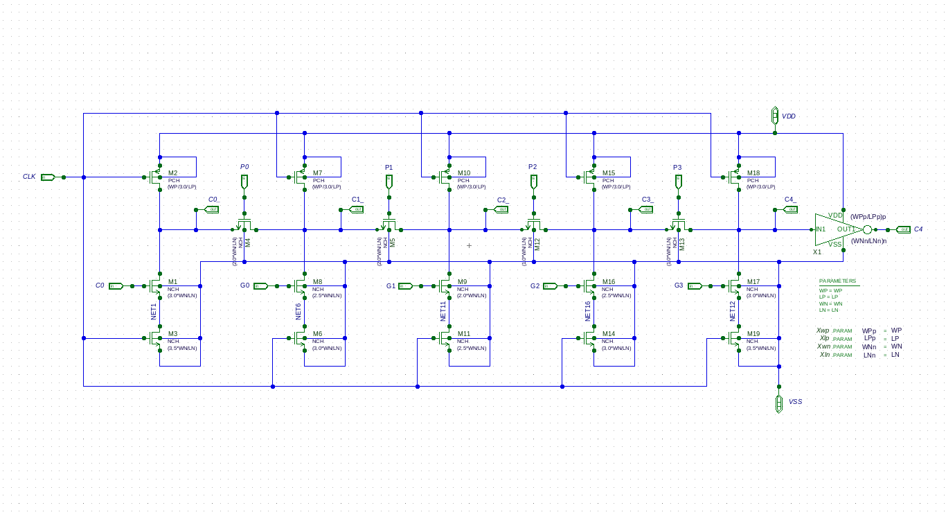
- Creating an optimized 4-Bit MCC circuit designed to handle 0.5pF load per internal-carry output signal.
- Creating a 4-Bit CLA Adder using the subcircuits identified above.
- Creating individual input decks to verify performance of all subcircuits and the full 4-Bit CLA Adder.
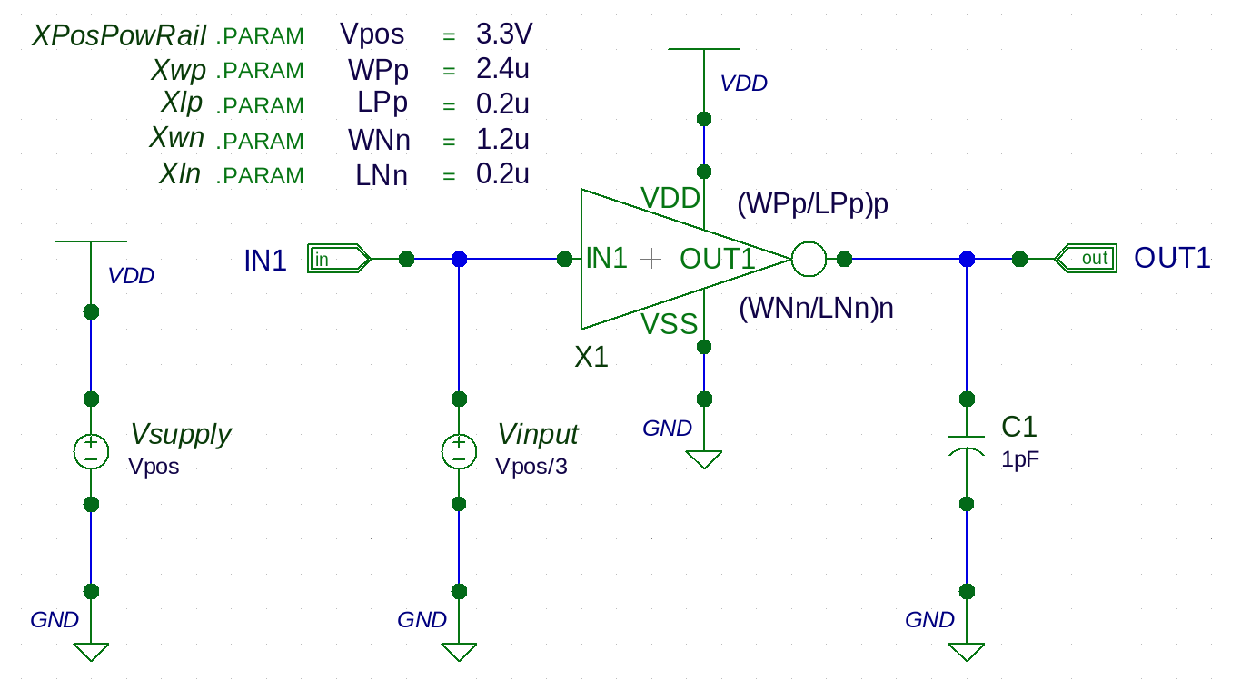
The INVERTER schematic illustrates the W/L ratios for the desired target performance. The INVERTER test schematic illustrates the INVERTER input deckused to simulate the transfer function (.DC analysis) and manually measure where the input voltage equals the output voltage. The INVERTER simulation output demonstrates these concepts.
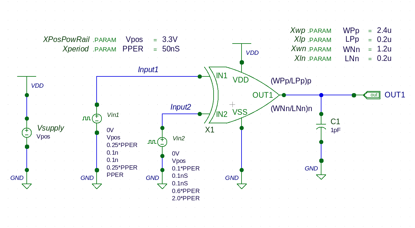
The 2-Input NAND schematic illustrates the W/L ratios for the desired target performance. The 2-Input NAND test schematic illustrates the 2-Input NAND input deckused to simulate the transient response (.TRANS analysis) and visually verify functionality. The 2-Input NAND simulation output demonstrates these concepts.
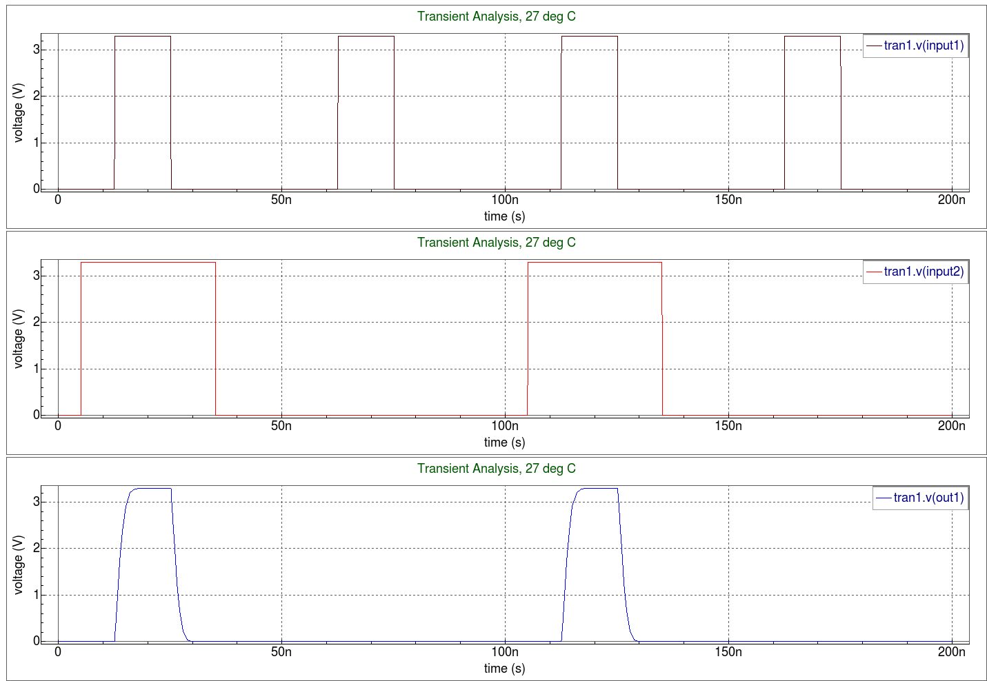
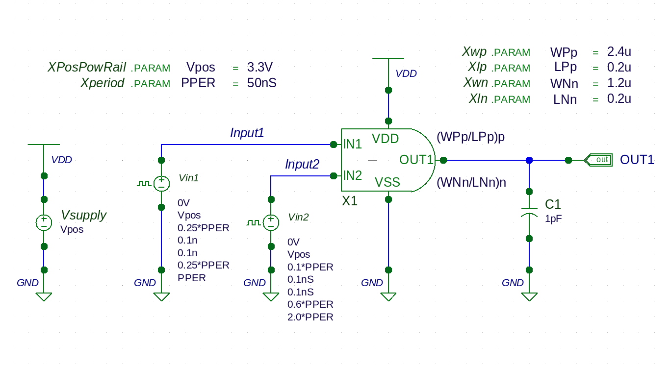
The 2-Input AND schematic illustrates the gate constructed from the INVERTER and the 2-Input NAND. The W/L ratios are inherited from these base gates to achieve the desired target performance. The 2-Input AND test schematic illustrates the 2-Input AND input deckused to simulate the transient response (.TRANS analysis) and visually verify functionality. The 2-Input AND simulation output demonstrates these concepts.
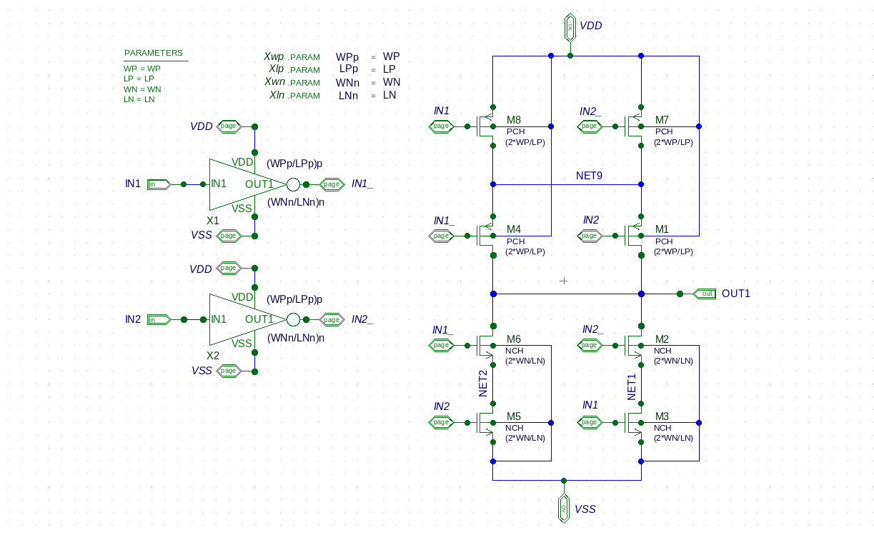
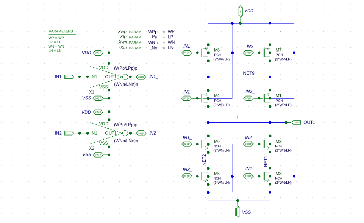
The 2-Input XNOR schematic and the 2-Input XOR schematic illustrate these gates constructed with the INVERTER and the W/L ratios sized to achieve the desired target performance. The 2-Input XNOR test schematic and the 2-Input XOR test schematic illustrate the 2-Input XNOR input deckand the 2-Input XOR input deckused to simulate the transient response (.TRANS analysis) and visually verify functionality for each gate. The 2-Input XNOR simulation output and the 2-Input XOR simulation output demonstrate these concepts.
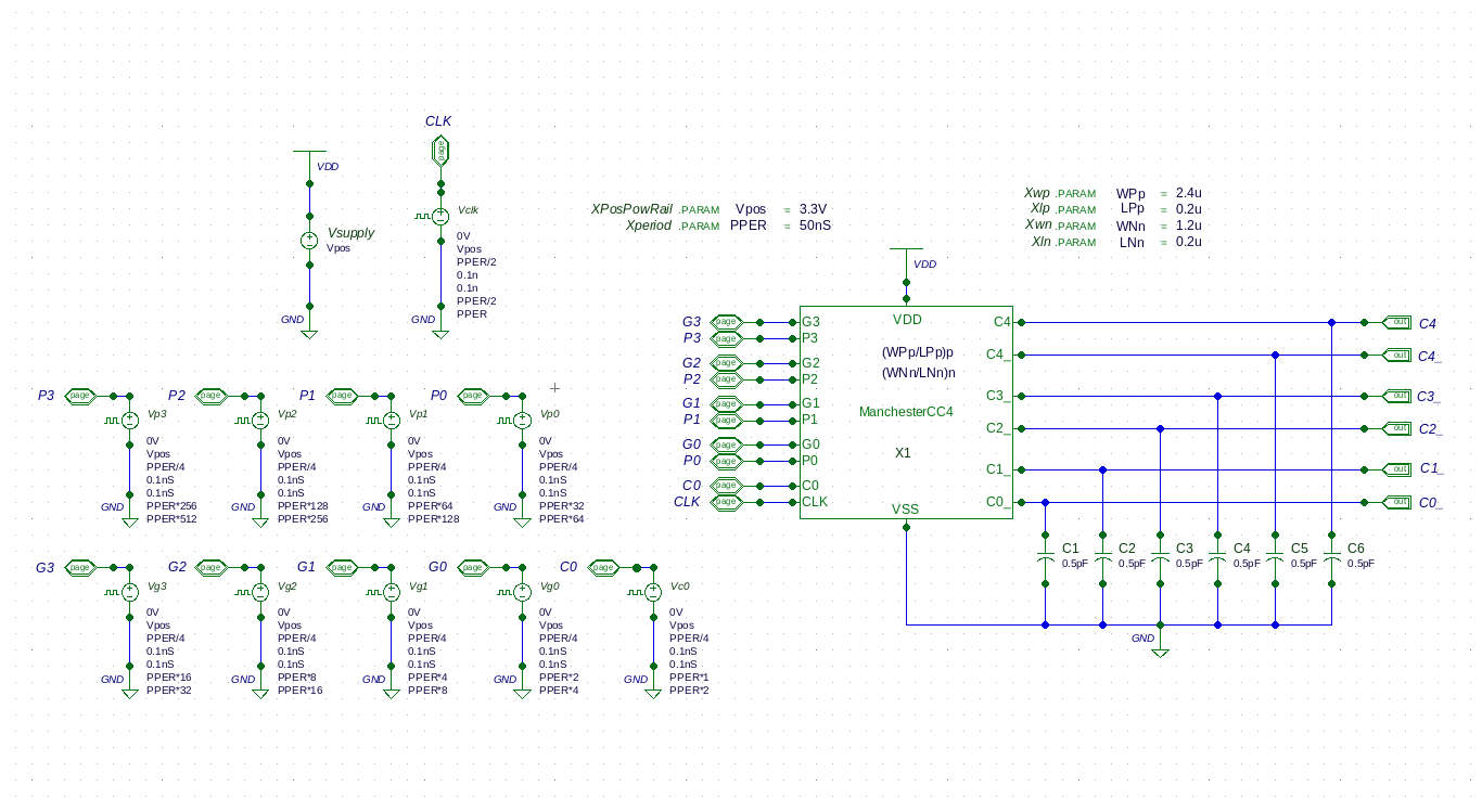
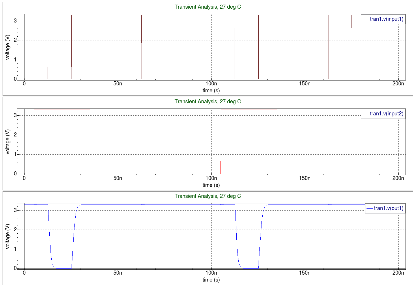
The MCC schematic illustrates the W/L ratios for the desired target performance. The MCC test schematic illustrates the MCC input deckused to simulate the transient response (.TRANS analysis) and visually verify functionality for all input combinations. The MCC simulation output demonstrates these concepts.
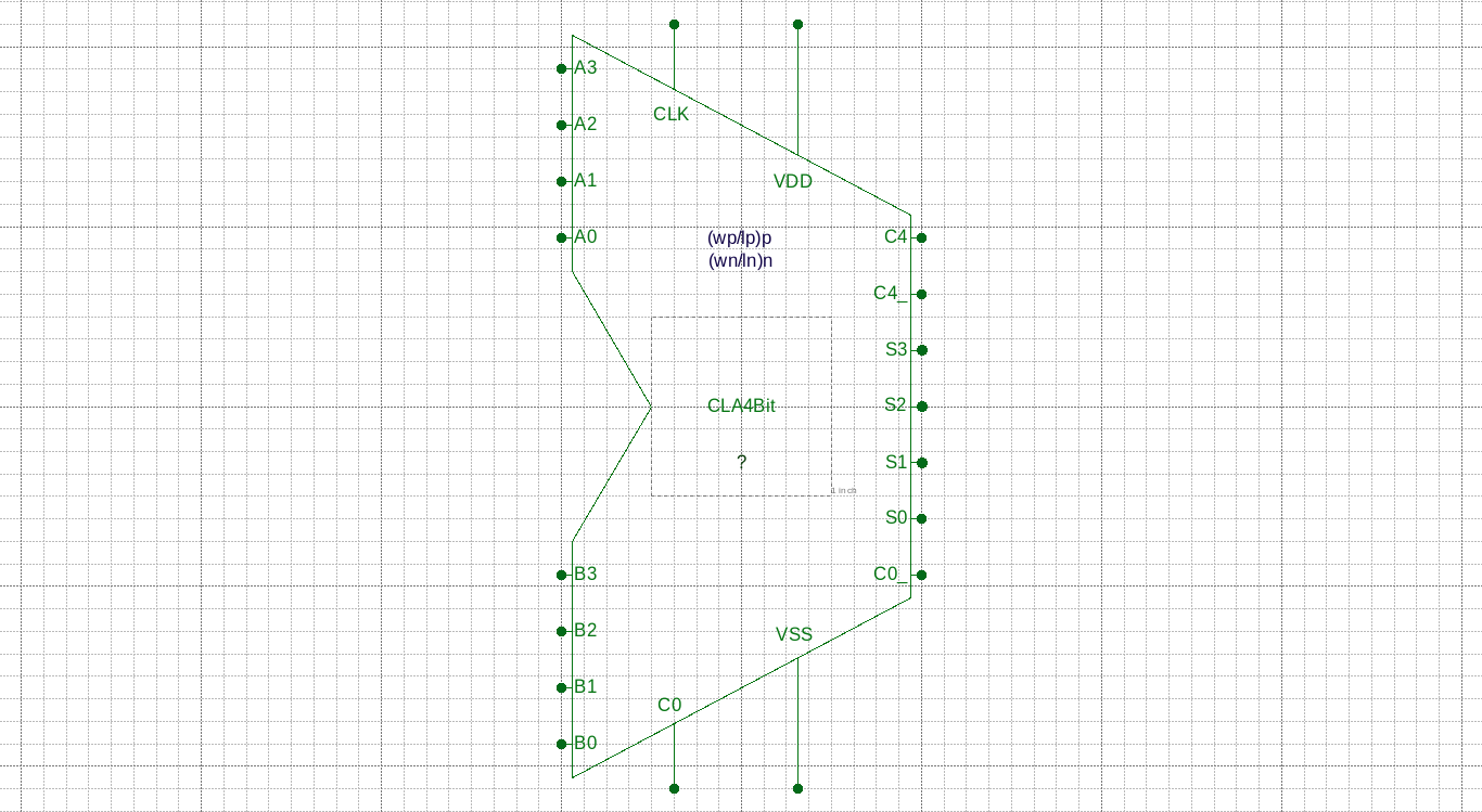
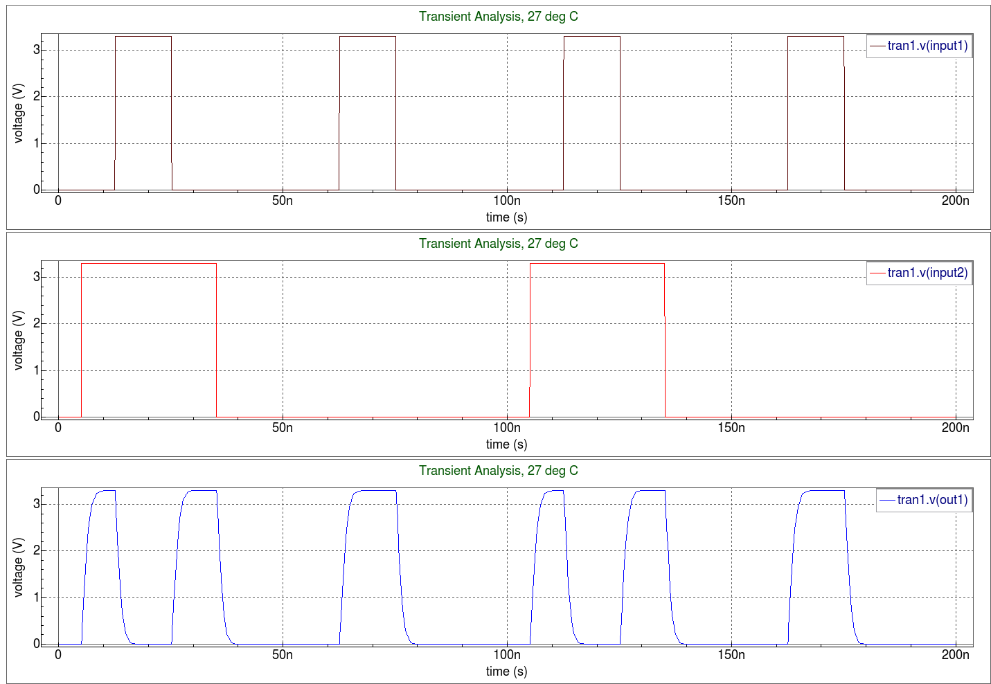
The 4-Bit CLA Adder schematic illustrates the full module constructed using the base subcircuits outlined previously (AND, XNOR, XOR, MCC). The 4-Bit CLA Adder test schematic illustrates the 4-Bit CLA Adder input deckused to simulate the transient response (.TRANS analysis) and visually verify functionality for all input combinations. The 4-Bit CLA Adder simulation output demonstrates these concepts.
test_and2.in
											* /home/CLA/test_and2
* Gateway 3.4.1.R Spice Netlist Generator
* Simulation timestamp: 07-Aug-2015 16:11:21
* Workspace name:       /home/CLA/CLA.workspace
* Simulation name:      /home/CLA/test_and2.schlr

* Schematic name: test_and2
X1 Input1 Input2 OUT1 VDD GND and2 LN=LNn LP=LPp WN=WNn WP=WPp
Vin2 Input2 GND PULSE(0V Vpos "0.1*PPER" 0.1nS 0.1nS "0.6*PPER" "2.0*PPER")
Vsupply VDD GND DC Vpos
Vin1 Input1 GND PULSE(0V Vpos "0.25*PPER" 0.1n 0.1n "0.25*PPER" PPER)
.PARAM Vpos=3.3V
.PARAM LNn=0.2u
.PARAM WPp=2.4u
.PARAM WNn=1.2u
.PARAM PPER=50nS
.PARAM LPp=0.2u
C1 OUT1 GND 1pF

* Schematic name: and2
.SUBCKT and2 IN1 IN2 OUT1 VDD VSS
.PARAM LNn=LN
.PARAM LPp=LP
.PARAM WNn=WN
.PARAM WPp=WP
X2 OUT_Nand2 OUT1 VDD VSS inverter LN=LNn LP=LPp WN=WNn WP=WPp
X1 IN1 IN2 OUT_Nand2 VDD VSS nand2 LN=LNn LP=LPp WN=WNn WP=WPp
.ENDS and2

* Schematic name: inverter
.SUBCKT inverter IN1 OUT1 VDD VSS
M2 OUT1 IN1 VDD VDD PCH L=LP W=WP
M1 OUT1 IN1 VSS VSS NCH L=LN W=WN
.ENDS inverter

* Schematic name: nand2
.SUBCKT nand2 IN1 IN2 OUT1 VDD VSS
M4 OUT1 IN1 VDD VDD PCH L=LP W=WP
M3 NET1 IN2 VSS VSS NCH L=LN W="2*WN"
M1 OUT1 IN2 VDD VDD PCH L=LP W=WP
M2 OUT1 IN1 NET1 VSS NCH L=LN W="2*WN"
.ENDS nand2

* Global Nodes Declarations
.GLOBAL GND

* End of the netlist

*
* Markers to save
*
.SAVE I(X1.VDD) I(Vsupply) V(Input1) V(Input2) V(OUT1)

* Schematic Netlist rebuilt at runtime

************* AND2 SIM - TRANSISTOR LEVEL ***********
*
*
**** MODEL CARDS ******
*
.include "./cla_transistor_models.inc"

*
*
*
**** ANALYSIS *****
.tran 0.001n PPER*4.0 0n 1n


.END
test_CLA_4Bit.in
											* /home/CLA/CLA_4Bit
* Gateway 3.4.1.R Spice Netlist Generator
* Simulation timestamp: 26-Aug-2015 10:33:16
* Workspace name:       /home/CLA/CLA.workspace
* Simulation name:      /home/CLA/CLA_4Bit.schlr

* Schematic name: CLA_4Bit
.PARAM LNn=0.2u
.PARAM Vpos=3.3V
.PARAM PPER=50nS
.PARAM WNn=1.2u
.PARAM LPp=0.2u
.PARAM WPp=2.4u
X1 A0 A1 A2 A3 B0 B1 B2 B3 C0 C4 C0_ C4_ CLK S0 S1 S2 S3 VDD GND CLA4Bit LN=LNn
+ LP=LPp WN=WNn WP=WPp
C7 C4 GND 1pF
C6 C4_ GND 1pF
C5 S3 GND 1pF
C4 S2 GND 1pF
C3 S1 GND 1pF
C2 S0 GND 1pF
Vc0 C0 GND PULSE(0V Vpos "PPER/4" 0.1nS 0.1nS "PPER*256" "PPER*512")
Vb3 B3 GND PULSE(0V Vpos "PPER/4" 0.1nS 0.1nS "PPER*128" "PPER*256")
Va3 A3 GND PULSE(0V Vpos "PPER/4" 0.1nS 0.1nS "PPER*64" "PPER*128")
Vb2 B2 GND PULSE(0V Vpos "PPER/4" 0.1nS 0.1nS "PPER*32" "PPER*64")
Va2 A2 GND PULSE(0V Vpos "PPER/4" 0.1nS 0.1nS "PPER*16" "PPER*32")
Vb1 B1 GND PULSE(0V Vpos "PPER/4" 0.1nS 0.1nS "PPER*8" "PPER*16")
Va1 A1 GND PULSE(0V Vpos "PPER/4" 0.1nS 0.1nS "PPER*4" "PPER*8")
Vb0 B0 GND PULSE(0V Vpos "PPER/4" 0.1nS 0.1nS "PPER*2" "PPER*4")
Va0 A0 GND PULSE(0V Vpos "PPER/4" 0.1nS 0.1nS "PPER*1" "PPER*2")
Vclk CLK GND PULSE(0V Vpos "PPER/2" 0.1n 0.1n "PPER/2" PPER)
C1 C0_ GND 1pF
Vsupply VDD GND DC Vpos

* Schematic name: and2
.SUBCKT and2 IN1 IN2 OUT1 VDD VSS
.PARAM LNn=LN
.PARAM LPp=LP
.PARAM WNn=WN
.PARAM WPp=WP
X2 OUT_Nand2 OUT1 VDD VSS inverter LN=LNn LP=LPp WN=WNn WP=WPp
X1 IN1 IN2 OUT_Nand2 VDD VSS nand2 LN=LNn LP=LPp WN=WNn WP=WPp
.ENDS and2

* Schematic name: CLA4Bit
.SUBCKT CLA4Bit A0 A1 A2 A3 B0 B1 B2 B3 C0 C4 C0_ C4_ CLK S0 S1 S2 S3 VDD VSS
.PARAM WPp=WP
.PARAM LNn=LN
.PARAM WNn=WN
.PARAM LPp=LP
X22 A0 B0 P0 VDD VSS xor2 LN=LNn LP=LPp WN=WNn WP=WPp
X20 A1 B1 P1 VDD VSS xor2 LN=LNn LP=LPp WN=WNn WP=WPp
X19 A2 B2 P2 VDD VSS xor2 LN=LNn LP=LPp WN=WNn WP=WPp
X18 A3 B3 P3 VDD VSS xor2 LN=LNn LP=LPp WN=WNn WP=WPp
X17 A0 B0 G0 VDD VSS and2 LN=LNn LP=LPp WN=WNn WP=WPp
X8 A1 B1 G1 VDD VSS and2 LN=LNn LP=LPp WN=WNn WP=WPp
X7 A2 B2 G2 VDD VSS and2 LN=LNn LP=LPp WN=WNn WP=WPp
X6 A3 B3 G3 VDD VSS and2 LN=LNn LP=LPp WN=WNn WP=WPp
X1 C0 C4 C0_ C1_ C2_ C3_ C4_ CLK G0 G1 G2 G3 P0 P1 P2 P3 VDD VSS ManchesterCC4
+ LN=LNn LP=LPp WN=WNn WP=WPp
X5 C0 P0 S0 VDD VSS xor2 LN=LNn LP=LPp WN=WNn WP=WPp
X4 C1_ P1 S1 VDD VSS xnor2 LN=LNn LP=LPp WN=WNn WP=WPp
X3 P2 C2_ S2 VDD VSS xnor2 LN=LNn LP=LPp WN=WNn WP=WPp
X2 P3 C3_ S3 VDD VSS xnor2 LN=LNn LP=LPp WN=WNn WP=WPp
.ENDS CLA4Bit

* Schematic name: inverter
.SUBCKT inverter IN1 OUT1 VDD VSS
M2 OUT1 IN1 VDD VDD PCH L=LP W=WP
M1 OUT1 IN1 VSS VSS NCH L=LN W=WN
.ENDS inverter

* Schematic name: ManchesterCC4
.SUBCKT ManchesterCC4 C0 C4 C0_ C1_ C2_ C3_ C4_ CLK G0 G1 G2 G3 P0 P1 P2 P3 VDD
+ VSS
X1 C4_ C4 VDD VSS inverter LN=LNn LP=LPp WN=WNn WP=WPp
.PARAM LPp=LP
.PARAM WPp=WP
.PARAM WNn=WN
.PARAM LNn=LN
M17 C4_ G3 NET12 VSS NCH L=LN W="3.0*WN"
M18 C4_ CLK VDD VDD PCH L=LP W="WP/3.0"
M19 NET12 CLK VSS VSS NCH L=LN W="3.5*WN"
M9 C2_ G1 NET11 VSS NCH L=LN W="2.0*WN"
M10 C2_ CLK VDD VDD PCH L=LP W="WP/3.0"
M11 NET11 CLK VSS VSS NCH L=LN W="2.5*WN"
M12 C3_ P2 C2_ VSS NCH L=LN W="1.0*WN"
M13 C4_ P3 C3_ VSS NCH L=LN W="1.0*WN"
M14 NET16 CLK VSS VSS NCH L=LN W="3.0*WN"
M15 C3_ CLK VDD VDD PCH L=LP W="WP/3.0"
M16 C3_ G2 NET16 VSS NCH L=LN W="2.5*WN"
M5 C2_ P1 C1_ VSS NCH L=LN W="2.0*WN"
M6 NET6 CLK VSS VSS NCH L=LN W="3.0*WN"
M7 C1_ CLK VDD VDD PCH L=LP W="WP/3.0"
M8 C1_ G0 NET6 VSS NCH L=LN W="2.5*WN"
M4 C1_ P0 C0_ VSS NCH L=LN W="2.0*WN"
M3 NET1 CLK VSS VSS NCH L=LN W="3.5*WN"
M2 C0_ CLK VDD VDD PCH L=LP W="WP/3.0"
M1 C0_ C0 NET1 VSS NCH L=LN W="3.0*WN"
.ENDS ManchesterCC4

* Schematic name: nand2
.SUBCKT nand2 IN1 IN2 OUT1 VDD VSS
M4 OUT1 IN1 VDD VDD PCH L=LP W=WP
M3 NET1 IN2 VSS VSS NCH L=LN W="2*WN"
M1 OUT1 IN2 VDD VDD PCH L=LP W=WP
M2 OUT1 IN1 NET1 VSS NCH L=LN W="2*WN"
.ENDS nand2

* Schematic name: xnor2
.SUBCKT xnor2 IN1 IN2 OUT1 VDD VSS
.PARAM WPp=WP
.PARAM LNn=LN
.PARAM LPp=LP
.PARAM WNn=WN
X2 IN2 IN2_ VDD VSS inverter LN=LNn LP=LPp WN=WNn WP=WPp
X1 IN1 IN1_ VDD VSS inverter LN=LNn LP=LPp WN=WNn WP=WPp
M7 NET9 IN2_ VDD VDD PCH L=LP W="2*WP"
M8 NET9 IN1 VDD VDD PCH L=LP W="2*WP"
M5 NET2 IN2 VSS VSS NCH L=LN W="2*WN"
M6 OUT1 IN1_ NET2 VSS NCH L=LN W="2*WN"
M4 OUT1 IN1_ NET9 VDD PCH L=LP W="2*WP"
M3 NET1 IN1 VSS VSS NCH L=LN W="2*WN"
M1 OUT1 IN2 NET9 VDD PCH L=LP W="2*WP"
M2 OUT1 IN2_ NET1 VSS NCH L=LN W="2*WN"
.ENDS xnor2

* Schematic name: xor2
.SUBCKT xor2 IN1 IN2 OUT1 VDD VSS
.PARAM LNn=LN
.PARAM LPp=LP
.PARAM WPp=WP
.PARAM WNn=WN
X2 IN2 IN2_ VDD VSS inverter LN=LNn LP=LPp WN=WNn WP=WPp
X1 IN1 IN1_ VDD VSS inverter LN=LNn LP=LPp WN=WNn WP=WPp
M7 NET9 IN2 VDD VDD PCH L=LP W="2*WP"
M8 NET9 IN1 VDD VDD PCH L=LP W="2*WP"
M5 NET2 IN2_ VSS VSS NCH L=LN W="2*WN"
M6 OUT1 IN1_ NET2 VSS NCH L=LN W="2*WN"
M4 OUT1 IN1_ NET9 VDD PCH L=LP W="2*WP"
M3 NET1 IN1 VSS VSS NCH L=LN W="2*WN"
M1 OUT1 IN2_ NET9 VDD PCH L=LP W="2*WP"
M2 OUT1 IN2 NET1 VSS NCH L=LN W="2*WN"
.ENDS xor2

* Global Nodes Declarations
.GLOBAL GND

* End of the netlist

*
* Markers to save
*
.SAVE I(X1.VDD) I(Vsupply) V(A0) V(A1) V(A2) V(A3) V(B0) V(B1) V(B2) V(B3) V(C0) V(C4) V(C0_) V(C4_) V(CLK) V(S0) V(S1) V(S2) V(S3)

* Schematic Netlist rebuilt at runtime

************* CLA_4BIT SIM - TRANSISTOR LEVEL ***********
*
*

**** MODEL CARDS ******
*
.include "./cla_transistor_models.inc"

*
*
**** ANALYSIS *****
.tran 0.001n PPER*600 0n 1n


.END
test_inverter.in
											* /home/CLA/test_inverter
* Gateway 3.4.1.R Spice Netlist Generator
* Simulation timestamp: 07-Aug-2015 15:16:27
* Workspace name:       /home/CLA/CLA.workspace
* Simulation name:      /home/CLA/test_inverter.schlr

* Schematic name: test_inverter
X1 IN1 OUT1 VDD GND inverter LN=LNn LP=LPp WN=WNn WP=WPp
.PARAM LNn=0.2u
.PARAM WNn=1.2u
.PARAM LPp=0.2u
.PARAM WPp=2.4u
.PARAM Vpos=3.3V
C1 OUT1 GND 1pF
Vinput IN1 GND DC "Vpos/3"
Vsupply VDD GND DC Vpos

* Schematic name: inverter
.SUBCKT inverter IN1 OUT1 VDD VSS
M2 OUT1 IN1 VDD VDD PCH L=LP W=WP
M1 OUT1 IN1 VSS VSS NCH L=LN W=WN
.ENDS inverter

* Global Nodes Declarations
.GLOBAL GND

* End of the netlist

*
* Markers to save
*
.SAVE I(X1.VDD) I(Vsupply) V(IN1) V(OUT1)

* Schematic Netlist rebuilt at runtime

************* INVERTER SIM - TRANSISTOR LEVEL ***********
*
*
**** MODEL CARDS ******
*
.include "./cla_transistor_models.inc"

*
*
*
**** ANALYSIS *****
.dc Vinput 0 Vpos 0.001

.END
test_ManchesterCC4.in
											* /home/CLA/test_ManchesterCC4
* Gateway 3.4.1.R Spice Netlist Generator
* Simulation timestamp: 07-Aug-2015 16:48:29
* Workspace name:       /home/CLA/CLA.workspace
* Simulation name:      /home/CLA/test_ManchesterCC4.schlr

* Schematic name: test_ManchesterCC4
.PARAM PPER=50nS
.PARAM WNn=1.2u
.PARAM LPp=0.2u
.PARAM LNn=0.2u
.PARAM WPp=2.4u
.PARAM Vpos=3.3V
X1 C0 C4 C0_ C1_ C2_ C3_ C4_ CLK G0 G1 G2 G3 P0 P1 P2 P3 VDD GND ManchesterCC4
+ LN=LNn LP=LPp WN=WNn WP=WPp
C6 C4 GND 0.5pF
C5 C4_ GND 0.5pF
C4 C3_ GND 0.5pF
C3 C2_ GND 0.5pF
C2 C1_ GND 0.5pF
Vp3 P3 GND PULSE(0V Vpos "PPER/4" 0.1nS 0.1nS "PPER*256" "PPER*512")
Vp2 P2 GND PULSE(0V Vpos "PPER/4" 0.1nS 0.1nS "PPER*128" "PPER*256")
Vp1 P1 GND PULSE(0V Vpos "PPER/4" 0.1nS 0.1nS "PPER*64" "PPER*128")
Vp0 P0 GND PULSE(0V Vpos "PPER/4" 0.1nS 0.1nS "PPER*32" "PPER*64")
Vg3 G3 GND PULSE(0V Vpos "PPER/4" 0.1nS 0.1nS "PPER*16" "PPER*32")
Vg2 G2 GND PULSE(0V Vpos "PPER/4" 0.1nS 0.1nS "PPER*8" "PPER*16")
Vg1 G1 GND PULSE(0V Vpos "PPER/4" 0.1nS 0.1nS "PPER*4" "PPER*8")
Vg0 G0 GND PULSE(0V Vpos "PPER/4" 0.1nS 0.1nS "PPER*2" "PPER*4")
Vc0 C0 GND PULSE(0V Vpos "PPER/4" 0.1nS 0.1nS "PPER*1" "PPER*2")
Vclk CLK GND PULSE(0V Vpos "PPER/2" 0.1n 0.1n "PPER/2" PPER)
C1 C0_ GND 0.5pF
Vsupply VDD GND DC Vpos

* Schematic name: inverter
.SUBCKT inverter IN1 OUT1 VDD VSS
M2 OUT1 IN1 VDD VDD PCH L=LP W=WP
M1 OUT1 IN1 VSS VSS NCH L=LN W=WN
.ENDS inverter

* Schematic name: ManchesterCC4
.SUBCKT ManchesterCC4 C0 C4 C0_ C1_ C2_ C3_ C4_ CLK G0 G1 G2 G3 P0 P1 P2 P3 VDD
+ VSS
X1 C4_ C4 VDD VSS inverter LN=LNn LP=LPp WN=WNn WP=WPp
.PARAM LPp=LP
.PARAM WPp=WP
.PARAM WNn=WN
.PARAM LNn=LN
M17 C4_ G3 NET12 VSS NCH L=LN W="3.0*WN"
M18 C4_ CLK VDD VDD PCH L=LP W="WP/3.0"
M19 NET12 CLK VSS VSS NCH L=LN W="3.5*WN"
M9 C2_ G1 NET11 VSS NCH L=LN W="2.0*WN"
M10 C2_ CLK VDD VDD PCH L=LP W="WP/3.0"
M11 NET11 CLK VSS VSS NCH L=LN W="2.5*WN"
M12 C3_ P2 C2_ VSS NCH L=LN W="1.0*WN"
M13 C4_ P3 C3_ VSS NCH L=LN W="1.0*WN"
M14 NET16 CLK VSS VSS NCH L=LN W="3.0*WN"
M15 C3_ CLK VDD VDD PCH L=LP W="WP/3.0"
M16 C3_ G2 NET16 VSS NCH L=LN W="2.5*WN"
M5 C2_ P1 C1_ VSS NCH L=LN W="2.0*WN"
M6 NET6 CLK VSS VSS NCH L=LN W="3.0*WN"
M7 C1_ CLK VDD VDD PCH L=LP W="WP/3.0"
M8 C1_ G0 NET6 VSS NCH L=LN W="2.5*WN"
M4 C1_ P0 C0_ VSS NCH L=LN W="2.0*WN"
M3 NET1 CLK VSS VSS NCH L=LN W="3.5*WN"
M2 C0_ CLK VDD VDD PCH L=LP W="WP/3.0"
M1 C0_ C0 NET1 VSS NCH L=LN W="3.0*WN"
.ENDS ManchesterCC4

* Global Nodes Declarations
.GLOBAL GND

* End of the netlist

*
* Markers to save
*
.SAVE I(X1.VDD) I(Vsupply) V(C0) V(C4) V(C0_) V(C1_) V(C2_) V(C3_) V(C4_) V(CLK) V(G0) V(G1) V(G2) V(G3) V(P0) V(P1) V(P2) V(P3)

* Schematic Netlist rebuilt at runtime

************* ManchesterCC4 SIM - TRANSISTOR LEVEL ***********
*
*
**** MODEL CARDS ******
*
.include "./cla_transistor_models.inc"

*
*
*
**** ANALYSIS *****
.tran 0.001n PPER*600 0n 1n


.END
test_nand2.in
											* /home/CLA/test_nand2
* Gateway 3.4.1.R Spice Netlist Generator
* Simulation timestamp: 07-Aug-2015 16:09:02
* Workspace name:       /home/CLA/CLA.workspace
* Simulation name:      /home/CLA/test_nand2.schlr

* Schematic name: test_nand2
.PARAM LNn=0.2u
.PARAM WNn=1.2u
.PARAM LPp=0.2u
.PARAM WPp=2.4u
X1 Input1 Input2 OUT1 VDD GND nand2 LN=LNn LP=LPp WN=WNn WP=WPp
.PARAM PPER=50nS
.PARAM Vpos=3.3V
Vin2 Input2 GND PULSE(0V Vpos "0.1*PPER" 0.1nS 0.1nS "0.6*PPER" "2.0*PPER")
Vin1 Input1 GND PULSE(0V Vpos "0.25*PPER" 0.1n 0.1n "0.25*PPER" PPER)
C1 OUT1 GND 1pF
Vsupply VDD GND DC Vpos

* Schematic name: nand2
.SUBCKT nand2 IN1 IN2 OUT1 VDD VSS
M4 OUT1 IN1 VDD VDD PCH L=LP W=WP
M3 NET1 IN2 VSS VSS NCH L=LN W="2*WN"
M1 OUT1 IN2 VDD VDD PCH L=LP W=WP
M2 OUT1 IN1 NET1 VSS NCH L=LN W="2*WN"
.ENDS nand2

* Global Nodes Declarations
.GLOBAL GND

* End of the netlist

*
* Markers to save
*
.SAVE I(X1.VDD) I(Vsupply) V(Input1) V(Input2) V(OUT1)

* Schematic Netlist rebuilt at runtime

************* NAND2 SIM - TRANSISTOR LEVEL ***********
*
*
**** MODEL CARDS ******
*
.include "./cla_transistor_models.inc"

*
*
*
**** ANALYSIS *****
.tran 0.001n PPER*4.0 0n 1n


.END
test_xnor2.in
											* /home/CLA/test_xnor2
* Gateway 3.4.1.R Spice Netlist Generator
* Simulation timestamp: 07-Aug-2015 16:12:12
* Workspace name:       /home/CLA/CLA.workspace
* Simulation name:      /home/CLA/test_xnor2.schlr

* Schematic name: test_xnor2
Vsupply VDD GND DC Vpos
Vin1 Input1 GND PULSE(0V Vpos "0.25*PPER" 0.1n 0.1n "0.25*PPER" PPER)
Vin2 Input2 GND PULSE(0V Vpos "0.1*PPER" 0.1nS 0.1nS "0.6*PPER" "2.0*PPER")
X1 Input1 Input2 OUT1 VDD GND xnor2 LN=LNn LP=LPp WN=WNn WP=WPp
.PARAM PPER=50nS
.PARAM WPp=2.4u
.PARAM Vpos=3.3V
.PARAM WNn=1.2u
.PARAM LNn=0.2u
.PARAM LPp=0.2u
C1 OUT1 GND 1pF

* Schematic name: inverter
.SUBCKT inverter IN1 OUT1 VDD VSS
M2 OUT1 IN1 VDD VDD PCH L=LP W=WP
M1 OUT1 IN1 VSS VSS NCH L=LN W=WN
.ENDS inverter

* Schematic name: xnor2
.SUBCKT xnor2 IN1 IN2 OUT1 VDD VSS
.PARAM WPp=WP
.PARAM LNn=LN
.PARAM LPp=LP
.PARAM WNn=WN
X2 IN2 IN2_ VDD VSS inverter LN=LNn LP=LPp WN=WNn WP=WPp
X1 IN1 IN1_ VDD VSS inverter LN=LNn LP=LPp WN=WNn WP=WPp
M7 NET9 IN2_ VDD VDD PCH L=LP W="2*WP"
M8 NET9 IN1 VDD VDD PCH L=LP W="2*WP"
M5 NET2 IN2 VSS VSS NCH L=LN W="2*WN"
M6 OUT1 IN1_ NET2 VSS NCH L=LN W="2*WN"
M4 OUT1 IN1_ NET9 VDD PCH L=LP W="2*WP"
M3 NET1 IN1 VSS VSS NCH L=LN W="2*WN"
M1 OUT1 IN2 NET9 VDD PCH L=LP W="2*WP"
M2 OUT1 IN2_ NET1 VSS NCH L=LN W="2*WN"
.ENDS xnor2

* Global Nodes Declarations
.GLOBAL GND

* End of the netlist

*
* Markers to save
*
.SAVE I(X1.VDD) I(Vsupply) V(Input1) V(Input2) V(OUT1)

* Schematic Netlist rebuilt at runtime

************* XNOR2 SIM - TRANSISTOR LEVEL ***********
*
*
**** MODEL CARDS ******
*
.include "./cla_transistor_models.inc"

*
*
*
**** ANALYSIS *****
.tran 0.001n PPER*4.0 0n 1n


.END
test_xor2.in
											* /home/CLA/test_xor2
* Gateway 3.4.1.R Spice Netlist Generator
* Simulation timestamp: 07-Aug-2015 16:13:13
* Workspace name:       /home/CLA/CLA.workspace
* Simulation name:      /home/CLA/test_xor2.schlr

* Schematic name: test_xor2
Vsupply VDD GND DC Vpos
Vin1 Input1 GND PULSE(0V Vpos "0.25*PPER" 0.1n 0.1n "0.25*PPER" PPER)
Vin2 Input2 GND PULSE(0V Vpos "0.1*PPER" 0.1nS 0.1nS "0.6*PPER" "2.0*PPER")
.PARAM WNn=1.2u
.PARAM Vpos=3.3V
.PARAM PPER=50nS
.PARAM LNn=0.2u
.PARAM LPp=0.2u
.PARAM WPp=2.4u
X1 Input1 Input2 OUT1 VDD GND xor2 LN=LNn LP=LPp WN=WNn WP=WPp
C1 OUT1 GND 1pF

* Schematic name: inverter
.SUBCKT inverter IN1 OUT1 VDD VSS
M2 OUT1 IN1 VDD VDD PCH L=LP W=WP
M1 OUT1 IN1 VSS VSS NCH L=LN W=WN
.ENDS inverter

* Schematic name: xor2
.SUBCKT xor2 IN1 IN2 OUT1 VDD VSS
.PARAM LNn=LN
.PARAM LPp=LP
.PARAM WPp=WP
.PARAM WNn=WN
X2 IN2 IN2_ VDD VSS inverter LN=LNn LP=LPp WN=WNn WP=WPp
X1 IN1 IN1_ VDD VSS inverter LN=LNn LP=LPp WN=WNn WP=WPp
M7 NET9 IN2 VDD VDD PCH L=LP W="2*WP"
M8 NET9 IN1 VDD VDD PCH L=LP W="2*WP"
M5 NET2 IN2_ VSS VSS NCH L=LN W="2*WN"
M6 OUT1 IN1_ NET2 VSS NCH L=LN W="2*WN"
M4 OUT1 IN1_ NET9 VDD PCH L=LP W="2*WP"
M3 NET1 IN1 VSS VSS NCH L=LN W="2*WN"
M1 OUT1 IN2_ NET9 VDD PCH L=LP W="2*WP"
M2 OUT1 IN2 NET1 VSS NCH L=LN W="2*WN"
.ENDS xor2

* Global Nodes Declarations
.GLOBAL GND

* End of the netlist

*
* Markers to save
*
.SAVE I(X1.VDD) I(Vsupply) V(Input1) V(Input2) V(OUT1)

* Schematic Netlist rebuilt at runtime

************* XOR2 SIM - TRANSISTOR LEVEL ***********
*
*
**** MODEL CARDS ******
*
.include "./cla_transistor_models.inc"

*
*
*
**** ANALYSIS *****
.tran 0.001n PPER*4.0 0n 1n


.END