003_abutment : Automatic Device Linking (Abutment)
Minimum Required Version: Expert 4.10.39.R
Device link improves the efficiency of layout design of CMOS logic circuits. By overlapping diffusion areas of MOSFET parameterized cells (PCells) that have a common net name, the PCells are automatically aligned and linked to each other.
It also recognizes whether an external connection exists from the connected pin and, if possible, can omit the diffusion contacts to minimize the spacing between the pair of gate regions.
In order to use the device link, a net name should be assigned to each pin on a MOSFET cell, as when it is supposed to be used within the schematic driven layout. Also, since the shapes of the diffusion area and contacts are controlled via PCell parameters, the MOSFET cell should be prepared as a PCell.
In addition, the device link requires a callback function written in LISA or JavaScript to control those PCell parameters. When multiple PCell instances are overlapped, or the Tools->Device Link->Link command is executed, this callback function is executed automatically so that each of the PCell parameters for the linked PCell instances is set.
The actual operation steps are as follows:
- Start Expert and select Tools->Script->Script Panel to open the XI script panel.
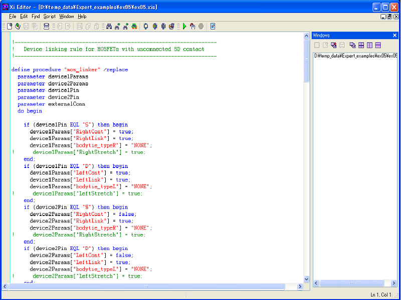
- Select File->Open in the XI script panel to load a sample XI script editing_ex03.xisand run it. It defines the callback function for the device link (see 1_script_panel.png ).
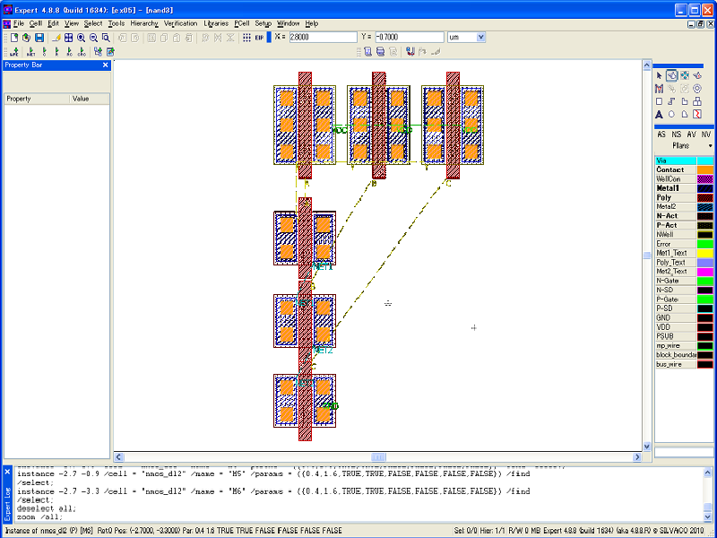
- Select File->Open in the Expert main window to load a project file exp_example_05.eld, and open the top cell NAND3.
- Select Tools->Netlist Driven Layout->Show Nets . Flight lines are displayed to indicate interconnect information between the placed PCell instances (see 2_initial_placement.png ).
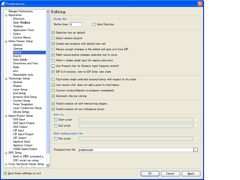
- Select Setup->Editor/Viewer to open the Preferences dialog.
- Open the Edit page in the dialog, check the Automatic Device Linking checkbox, and click OK to close the dialog (see 3_setup_dialog.png ).
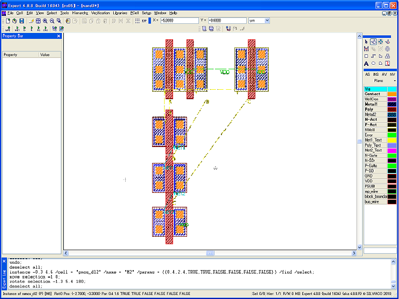
- Select a PCell instance of the cell CMOSP, which is placed in the middle of the upper row.
- Select Edit->Move to start moving the selected instance.
- Click the right mouse button twice to rotate it by 180 degrees. As a result, a pair of pins on the diffusion areas sharing a same net name will face each other.
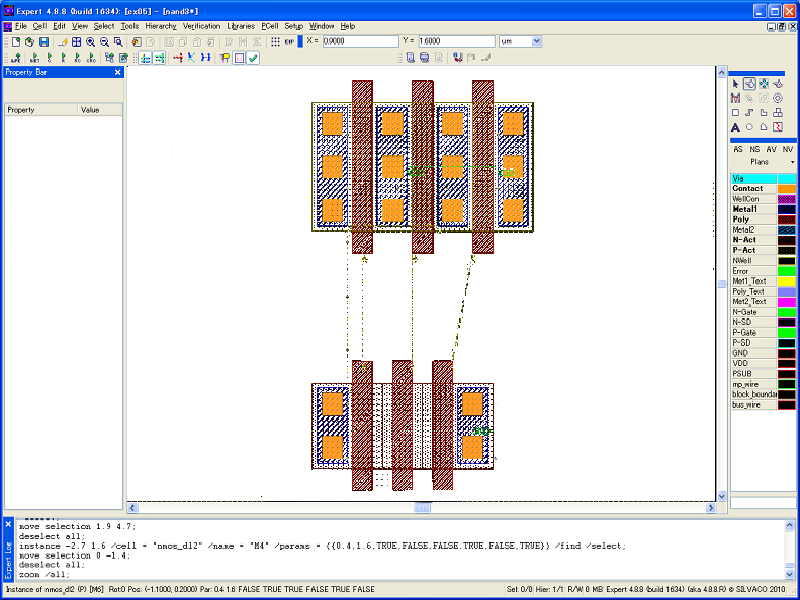
- Place the selected instance in order that the diffusion areas are overlapped with each other. The overlapped instances will be linked to each other automatically (see 4_link_cmosp.png ).
- Link the remaining instance at the right side as well.
- Repeat the same operations for CMOSN PCell instances in the lower row.
Since some of the connected pins don't have any external connections,s the contact objects between gates will be deleted, and the spacing between the gates will be minimized as defined in advance (see 5_link_cmosn.png ).
editing_ex03.xis
!------------------------------------------------------------------
!   Device linking rule for MOSFETs with unconnected SD contact
!------------------------------------------------------------------

define procedure "mos_linker" /replace
  parameter device1Params
  parameter device2Params
  parameter device1Pin
  parameter device2Pin
  parameter externalConn
  do begin

    if (device1Pin EQL "S") then begin
      device1Params["RightCont"] = true;
      device1Params["RightLink"] = true;
      device1Params["bodytie_typeR"] = "NONE";
!      device1Params["RightStretch"] = true;
    end;
    if (device1Pin EQL "D") then begin
      device1Params["LeftCont"] = true;
      device1Params["LeftLink"] = true;
      device1Params["bodytie_typeL"] = "NONE";
!      device1Params["LeftStretch"] = true;
    end;
    if (device2Pin EQL "S") then begin
      device2Params["RightCont"] = false;
      device2Params["RightLink"] = true;
      device2Params["bodytie_typeR"] = "NONE";
!      device2Params["RightStretch"] = true;
    end;
    if (device2Pin EQL "D") then begin
      device2Params["LeftCont"] = false;
      device2Params["LeftLink"] = true;
      device2Params["bodytie_typeL"] = "NONE";
!      device2Params["LeftStretch"] = true;
    end;

    if ((device1Pin EQL "S") and (device2Pin EQL "S")) then begin

!      device1Params["RightStretch"] = true;
!      device2Params["RightStretch"] = false;

    end;

    if ((device1Pin EQL "D") and (device2Pin EQL "D")) then begin

 !     device1Params["LeftStretch"] = true;
 !     device2Params["LeftStretch"] = false;

    end;

  end;

!------------------------------------------------------------------
!   Device linking rule for MOSFETs without unconnected SD contact
!------------------------------------------------------------------

define procedure "mos_linker_2" /replace
  parameter device1Params
  parameter device2Params
  parameter device1Pin
  parameter device2Pin
  parameter externalConn
  do begin

    if (device1Pin EQL "S") then begin
      device1Params["RightCont"] = externalConn;
      device1Params["RightLink"] = true;
      device1Params["bodytie_typeR"] = "NONE";
      device1Params["RightStretch"] = not externalConn;
    end;
    if (device1Pin EQL "D") then begin
      device1Params["LeftCont"] = externalConn;
      device1Params["LeftLink"] = true;
      device1Params["bodytie_typeL"] = "NONE";
      device1Params["LeftStretch"] = not externalConn;
    end;
    if (device2Pin EQL "S") then begin
      device2Params["RightCont"] = false;
      device2Params["RightLink"] = true;
      device2Params["bodytie_typeR"] = "NONE";
      device2Params["RightStretch"] = not externalConn;
    end;
    if (device2Pin EQL "D") then begin
      device2Params["LeftCont"] = false;
      device2Params["LeftLink"] = true;
      device2Params["bodytie_typeL"] = "NONE";
      device2Params["LeftStretch"] = not externalConn;
    end;

    if ((device1Pin EQL "S") and (device2Pin EQL "S")) then begin

!      device1Params["RightStretch"] = true;
!      device2Params["RightStretch"] = false;

    end;

    if ((device1Pin EQL "D") and (device2Pin EQL "D")) then begin

 !     device1Params["LeftStretch"] = true;
 !     device2Params["LeftStretch"] = false;

    end;

  end;

!------------------------------------------------------------------
!   Device linking rule for resistors
!------------------------------------------------------------------

define procedure "tsmc_res_linker" /replace
  parameter device1Params
  parameter device2Params
  parameter device1Pin
  parameter device2Pin
  parameter externalConn
  do begin

  display("device1Pin=" & device1Pin);
  display("device2Pin=" & device2Pin);


  if (device1Params["LinkDirection"] EQL "HORIZONTAL") then begin

    if (device1Pin EQL "P") then begin
      device1Params["RightLink"] = true;
    end;

    if (device1Pin EQL "N") then begin
      device1Params["LeftLink"] = true;
    end;

    if (device2Pin EQL "P") then begin
      device2Params["RightLink"] = true;
    end;

    if (device2Pin EQL "N") then begin
      device2Params["LeftLink"] = true;
    end;

  end;

  !-------------------------------------------------------------------
  !   for vertical link
  !-------------------------------------------------------------------

  if (device1Params["LinkDirection"] EQL "VERTICAL") then begin

    if (device1Pin NEQ device2Pin) then begin

      device2Params["SwapTerminals"] = not device2Params["SwapTerminals"];

      if (device1Pin EQL "P") then begin
        device1Params["RightLink"] = true;
      end;

      if (device1Pin EQL "N") then begin
        device1Params["LeftLink"] = true;
      end;

      if (device2Pin EQL "P") then begin
        device2Params["LeftLink"] = true;
      end;

      if (device2Pin EQL "N") then begin
        device2Params["RightLink"] = true;
      end;

    end;

    if ((device1Pin EQL device2Pin) and (device1Params["LinkDirection"] EQL "VERTICAL")) then begin

      device2Params["SwapTerminals"] = device2Params["SwapTerminals"];

      if (device1Pin EQL "P") then begin
        device1Params["RightLink"] = true;
      end;

      if (device1Pin EQL "N") then begin
        device1Params["LeftLink"] = true;
      end;

      if (device2Pin EQL "P") then begin
        device2Params["RightLink"] = true;
      end;

      if (device2Pin EQL "N") then begin
        device2Params["LeftLink"] = true;
      end;

    end;

  end; ! for vertical link

end;