clex25.in : Simulation versus Measurement
Requires: Clever, VictoryProcess
Minimum Versions: VictoryProcess: 7.22.1.R/Clever 3.11.20.R
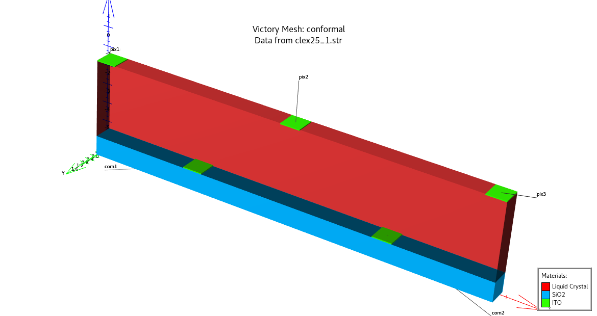
In this exampple, we will demonstrate how to simulate the dynamic LCD response using Clever LCD model and compared with reference data. In dynamic LCD mode, LC directors's response to input signal is the key point in a given Liquid Crystal material and electrode configuration. To get the time response of LC material, we employ VA(vertical Alignment) IPS(In-Plane-Switching) mode configuration. VA IPS LCD structure have three pixel electrodes at the same plane and two common electrode at the bottom surface. Two common electrode is grounded and two pixel electrodes are biased with same polarity. the centeral pixel electride(pix2) is biased on opposite polarity of "pix1" and "pix3".
Build 3D LCD structure using process simulator. First part of input is to make a 3D simulation structure using Victoryprocess process simulator. SpecifyMaskpoly statement define three pixel electrode and two common electrode which are normally grounded to zero. In Victoryprocess, Liquid crystal material is defined as user-defined material name "LC" and it is recognized as a liquid crystal material in Clever with liquid crystal parameters. Tonyplot3D plot show us generated three diemensional VA(Vertical Alignment) IPS(In-Plane-Switching) mode LCD structure. It consist of three Pixel electrodes at the top and two common electrodes at the bottom. User can simulate different gap, width of electrodes, and thickness of liquid crystal by modifying the value of 'g', 'w', and 'lc_thick' variable. The dimension of x is defined by "xmin" and "xmax" variable and ymin/ymax controll the dimension of y.
Electrical & Optical simulation of LC is performed in Clever.
First, we have to define LC's anisotropic permittivity, elastic constant, and rotation viscosity.
setPixelbias("pix2", 0,-0.5,-1,-1.5,-2,-2.5,-3,-3.5,-4,-4.5,-5,-5.5,-6,-6.5,-7,-7.5,-8) vmaxtrap=5
- which describe static dc bias on "pix2" electrode. It starts from 0 and end with -8 Volt
Interconnect Capacitance structure="clex25_dc" domainboundarycondition=cyclic skipcap
- perform dc static analysis in a given pixel voltage by "setpixelbias" command
setDynamicPixBias pixelfile="clex25_0.dat"
- it describe time pulse data from measurement file or other emulator.
Interconnect Capacitance structure="clex25_tran" domainboundarycondition=cyclic skipcap
- performs field solver calculation and save to file at each time. Clever appends .T'Time' clex25_tran filename at each time solution.
After getting solution for dc and transient, we plot voltage versus transmittance and contour of transmittance in each case.
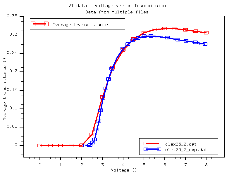
To get optical properties of LC's response during time pulse, we assumed crossed linear polarizers. "Optics" statement calculate the transmittance in given optical properties of material. To plot transmittance versus voltage, we extracted average transmittance value at DC bias and it is saved to clex25_2.dat file. Finally, tt is compared to measurement data(clex25_2_exp.dat).
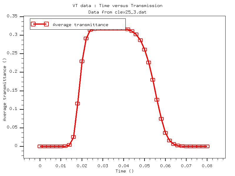
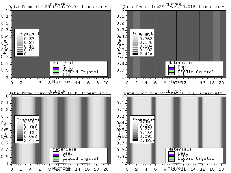
Finally, we plotted the time versus transmittance curve by assuming user-define input pulse(clex25_0.dat). It show typical transient behavior in rise time and falling time even symmetric steep input pulse is applied.
To load and run this example, select the Load example button in DeckBuild. This will copy the input file and any support files to your current working directory. Select the run button to execute the example.
Additional Info:
Input Deck
go VictoryProcess
#IPS-VA
# Liquid Crystal, Vol. 38, No. 4, April 2011, 507-510
# Fast-response vertical alignment liquid crystal display
# driven by in-plane switching
set spacing=2
set g=9
set w=1
set lc_thick=4
set xmin=0
set xmax=3*$w+2*$g
set ymin=0
set ymax=1
Init material="oxide" GasHeight=$lc_thick+2 Depth=1 \
from="$xmin,$ymin" to="$xmax,$ymax"
##################################################
# pixel electrode
# +V
SpecifyMaskPoly maskname=pixel p1="0,$ymin" p2="$w,$ymin" p3="$w,$ymax" p4="0,$ymax" electrode="pix1"
# -V
set x1=$w+$g
set x2=$w+$g+$w
SpecifyMaskPoly maskname=pixel p1="$x1,$ymin" p2="$x2,$ymin" p3="$x2,$ymax" p4="$x1,$ymax" electrode="pix2" add
# +V
set x1=2*$w+2*$g
set x2=3*$w+2*$g
SpecifyMaskPoly maskname=pixel p1="$x1,$ymin" p2="$x2,$ymin" p3="$x2,$ymax" p4="$x1,$ymax" electrode="pix3" add
set x1=$w+$g/2-$w/2
set x2=$x1+$w
# common
SpecifyMaskPoly maskname=common p1="$x1,$ymin" p2="$x2,$ymin" p3="$x2,$ymax" p4="$x1,$ymax" electrode="com1"
set x1=2*$w+$g+$g/2-$w/2
set x2=$x1+$w
# com2
SpecifyMaskPoly maskname=common p1="$x1,$ymin" p2="$x2,$ymin" p3="$x2,$ymax" p4="$x1,$ymax" electrode="com2" add
###################################################
line x position=0 spac=0.25
line x position=$w s=0.25
line x position=$w+$g/2 s=0.5
line x position=$w +$g s=0.25
line x position=$w+$g + $w s=0.25
line x position=$w+$g + $w + $g/2 s=0.5
line x position=$w+$g + $w + $g s=0.25
line x position=$xmax s=0.25
line y position=$ymin s=0.5
line y position=$ymax s=0.5
line z position=0 spacing=0.1
line z position=1 spacing=0.5
# VA-IPS
# pixel electrode
deposit material="ITO" thick=0.05 max
mask "pixel"
etch material="ITO" thick=0.05 min
strip
electrode material="ITO" mask="pixel"
# LC; cell gap 4um
deposit material="LC" thick=$lc_thick-0.05 min
# deposit material="LC" thick=$lc_thick min
# top common electrode
deposit material="ITO" thick=0.05 max
mask "common"
etch material="ITO" thick=0.05 max
strip
electrodes material="ITO" mask="common"
# electrodes material="ITO" name=com x=6 y=6 z=-4.025
deposit material="LC" thick=0.05 min
# sub
deposit oxide thick=1 max
line z loc=-5.0 s=0.5
line z loc=-$lc_thick s=0.1
line z loc=-$lc_thick+0.05 s=0.05
line z loc=-$lc_thick/2 s=0.5
line z loc=-0.05 s=0.05
line z loc=-0.0 s=0.1
save name=clex25_0
## Create a Conformal Mesh Structure File ##
go victorymesh
load in=clex25_0
remesh conformal
save out=clex25_1.str
tonyplot3d clex25_1.str -set clex25_0.set
# -png clex25_plot4.png
go clever
# read simulatioin structure
init structure="clex25_1.str"
# ITO metal conductivity
material ITO conductivity=1000
# LC properties
setLC epsParaDir=13.66 epsVertDir=3.66 splay=10.9e-12 twist=9.5e-12 bend=15.4e-12 \
cPenalty=1000 gama=0.1
# Specify the rubbing angle and the pre-tilt angle on the top and at the bottom of the LC region.
LCbndaryB partition(0 $xmax) rubAngle(0) tiltangle(90)
LCbndaryT partition(0 $xmax) rubAngle(0) tiltangle(90)
# numeric option
solver linearsolver=pam pamsolver=gmres ddprecond=RAS preconditioner=amp multilevel=0 \
fillratio=1e-4 lsmaxiter=100 lstolerance=1.0e-11 nlsmaxiter=100 nlstolerance=1.0e-8
option LSconvergeinfo=1 NLSconvergeinfo
setfixedbias "com1"=0 "com2"=0 numInitramp=5
setPixelbias("pix1", 0,0.5,1,1.5,2,2.5,3,3.5,4,4.5,5,5.5,6,6.5,7,7.5,8) vmaxtrap=5
setPixelbias("pix2", 0,-0.5,-1,-1.5,-2,-2.5,-3,-3.5,-4,-4.5,-5,-5.5,-6,-6.5,-7,-7.5,-8) vmaxtrap=5
setPixelbias("pix3", 0,0.5,1,1.5,2,2.5,3,3.5,4,4.5,5,5.5,6,6.5,7,7.5,8) vmaxtrap=5
# solve DC solution for plotting voltage versus transmittance
Interconnect Capacitance structure="clex25_dc" domainboundarycondition=cyclic skipcap
# Solve Transient
# loads pulse table
setDynamicPixBias pixelfile ="clex25_0.dat" vmaxtrap=5
Interconnect Capacitance structure="clex25_tran" domainboundarycondition=cyclic skipcap
# setdynamic waveform sinusoid elecname="pix1" tamplitude=6 \
# tfrequency=$freq tphase=0 tdecay=0.0
# Optical analysis
go clever
Init structure = "clex25_1.str"
system rm clex25_2.dat
system echo "VT data : Voltage versus Transmission" >> clex25_2.dat
system echo "17 2 2" >> clex25_2.dat
system echo "Voltage" >> clex25_2.dat
system echo "Average transmittance" >> clex25_2.dat
set V=0
loop steps=17
optics structure="clex25_dc.V$'V'.str" indexfile="clex25_1.dat" pixelvolt=$'V' \
wavelength=0.55 angle=0 theta=0 lightorient=frombot dx=0.125 dy=0.125 dzmax=0.025 \
topview="clex25_dc.V$'V'_linear" \
StartEndLayers(220, 45, 1.5, 1.5, 0.0044, 0; 220, -45, 1.5, 1.5, 0.0044, 0)
### average transmittance
extract init infile="clex25_dc.V$'V'_linear.str"
extract name="trans" 2d.area x.step=0.125 impurity="Transmittance" \
material="SiO2" y.min=$ymin y.max=$ymax x.min=0 x.max=$xmax
set ymax=abs($ymax-$ymin)
set ave_trans=$trans/($xmax*1e-4*$ymax*1e-4*1e-4)
# write to vt.dat file
system echo $'V' $'ave_trans' >> clex25_2.dat
set V=$V+0.5
l.end
# plot transmittance versus Voltage from dc solution
tonyplot -overlay clex25_2.dat clex25_2_exp.dat
# -png clex25_plot0.png
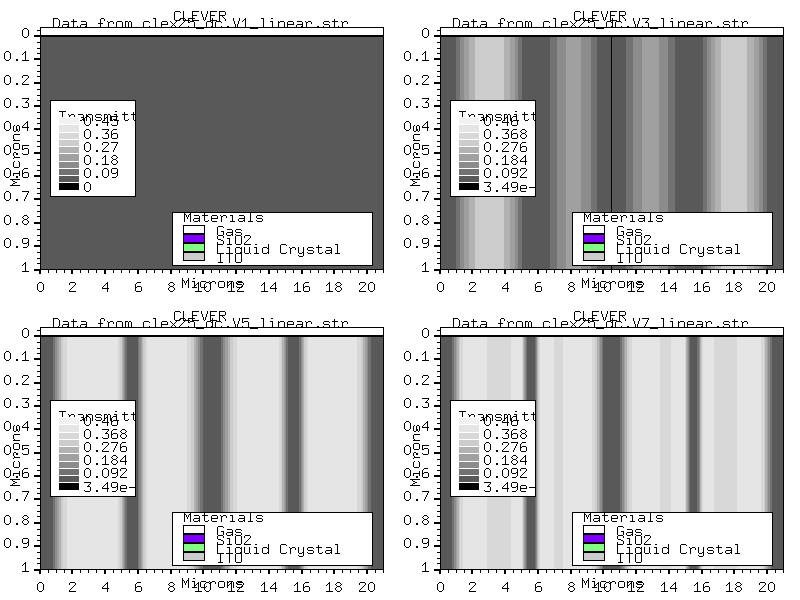
tonyplot clex25_dc.V1_linear.str clex25_dc.V3_linear.str clex25_dc.V5_linear.str clex25_dc.V7_linear.str -set clex25_1.set
# -png clex25_plot1.png
## for Transient ###
go clever
Init structure="clex25_1.str"
system rm clex25_3.dat
system echo "VT data : Time versus Transmission" >> clex25_3.dat
system echo "41 2 2" >> clex25_3.dat
system echo "Time" >> clex25_3.dat
system echo "Average transmittance" >> clex25_3.dat
set Time=0
loop steps=41
optics structure="clex25_tran.T$'Time'.str" indexfile="clex25_1.dat" \
wavelength=0.55 angle=0 theta=0 lightorient=frombot \
dx=0.125 dy=0.125 dzmax=0.025 topview="clex25_tran.T$'Time'_linear" \
StartEndLayers(220, 45, 1.5, 1.5, 0.0044, 0; 220, -45, 1.5, 1.5, 0.0044, 0)
### average transmittance
extract init infile="clex25_tran.T$'Time'_linear.str"
extract name="trans" 2d.area x.step=0.125 impurity="Transmittance" \
material="SiO2" y.min=$ymin y.max=$ymax x.min=0 x.max=$xmax
set ymax=abs($ymax-$ymin)
set ave_trans=$trans/($xmax*1e-4*$ymax*1e-4*1e-4)
#write to vt.dat file
system echo $'Time' $'ave_trans' >> clex25_3.dat
set Time=$Time+0.002
l.end
tonyplot clex25_3.dat
#-png clex25_plot2.png
tonyplot clex25_tran.T0.01_linear.str clex25_tran.T0.016_linear.str clex25_tran.T0.02_linear.str clex25_tran.T0.03_linear.str -set clex25_1.set
#-png clex25_plot3.png
quit