clex24.in : Dynamic Response Simulation of Liquid Crystal
Requires: Clever, Victoryprocess
Minimum Versions: VictoryProcess: 7.22.1.R/Clever 3.11.20.R
In this exampple, we will demonstrate how to simulate the dynamic LCD response using Clever LCD model. In dynamic LCD mode, LC directors's response to input signal is the key point in a given Liquid Crystal material and electrode configuration. To get the time response of LC material, we employ IPS(In-Plane-Switching) mode configuration. We demonstrate time dependent capacitance curve among electrodes and two dimensional transmittance contour at specific time where LC response is measured at rising, peak, and falling time. Addtionally, we simulated the transmittance curve with time which is very important characteristics of LCD.
Build 3D LCD structure using process simulator. First part of input is to make a 3D simulation structure using Victoryprocess process simulator. SpecifyMaskpoly statement define three pixel electrode and three common electrode which are normally grounded to zero. In Victoryprocess, Liquid crystal material is defined as user-defined material name "LC" and it is recognized as a liquid crystal material in Clever with liquid crystal parameters. Tonyplot3D plot show us generated three diemensional IPS(In-Plane-Switching) mode LCD structure. It consist of three Pixel electrodes and common electrodes.
Electrical & Optical simulation of LC is performed in Clever.
Before capacitance calculation, user need to define LC's anisotropic permittivity, elastic constant, and rotation viscosity.
setDynamicPixBias pixelfile="clex24_pulse.txt"
- it describes time pulse data from measurement file or other emulator.
Interconnect Capacitance domainboundarycondition=cyclic log="clex24_ips_3pix" structure="clex24_ips_3pix"
- performs field solver calculation and save to file at each time. Log="*" saves voltage of each electride as well as capacitance at simulated time.
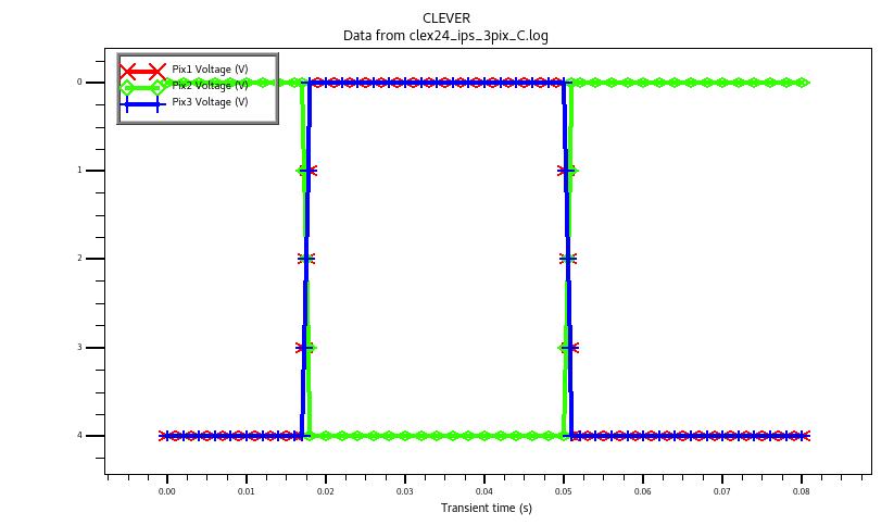
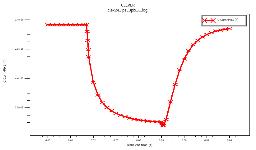
As of post-processing, we plot pulsed pixel electrode voltage at each time, which are described in pixelfile="*" file. "Pix1" and "Pix2" are biased on 4V whiile "Pix2" is bias on zero voltage. As you can see in capacitance versus time plot, the time responsive capacitance curve of between "Pix2" and "Com" show us typical time delay as respect to input pulse.
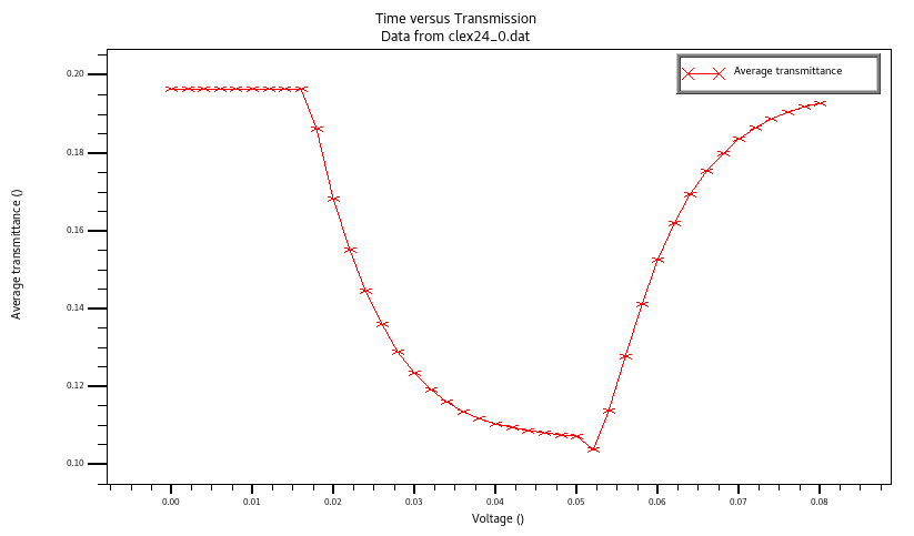
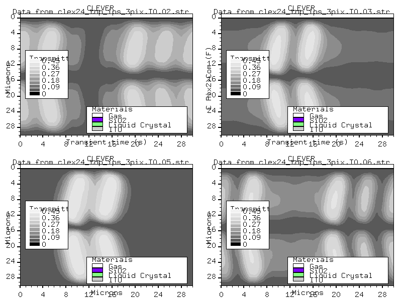
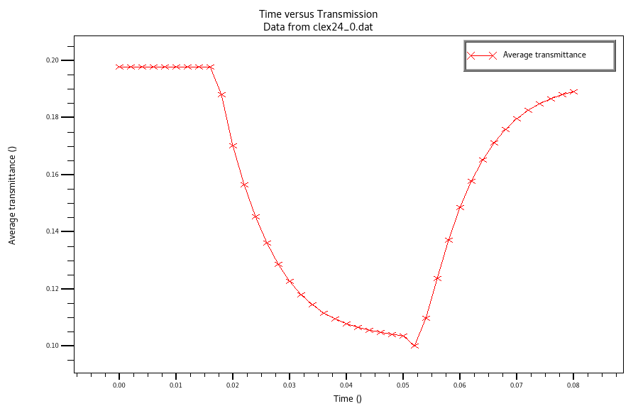
To get optical properties of LC's response during time pulse, We assumed ideal linear polarizers with LC's refactive index at 550nm wavelength. "Optics" statement calculate the transmittance in given optical properties of material. We plot two dimensional transmittance contour at each time where "Pix2" electrode is biased on at corresponding pixel voltage at this time. To plot transmittance versus time, we extracted average transmittance value at each time and it is saved to clex24_0.dat file.
To load and run this example, select the Load example button in DeckBuild. This will copy the input file and any support files to your current working directory. Select the run button to execute the example.
Additional Info:
Input Deck
											# This example demonstrates the LC director calculation of
# an in-plane switching (IPS) cell. The pixel layout of
# the IPS sub-pixel cell consists of two zigzag electrodes.
# A full-size pixel cell is composed of three sub-pixel cells.

go VictoryProcess

Init  material="oxide" GasHeight=5 Depth=1  from="0,0" to="30,30"

SpecifyMaskPoly maskname=ELEC p1="2.5,1" p2="0.5,15" p3="2.5,29" p4="4.5,29" p5="2.5,15" p6="4.5,1" electrode="Pix1"
SpecifyMaskPoly maskname=ELEC p1="12.5,1" p2="10.5,15" p3="12.5,29" p4="14.5,29" p5="12.5,15" p6="14.5,1" electrode="Pix2" add
SpecifyMaskPoly maskname=ELEC p1="22.5,1" p2="20.5,15" p3="22.5,29" p4="24.5,29" p5="22.5,15" p6="24.5,1" electrode="Pix3" add
SpecifyMaskPoly maskname=ELEC p1="7.5,1" p2="5.5,15" p3="7.5,29" p4="9.5,29" p5="7.5,15" p6="9.5,1" electrode="Com" add
SpecifyMaskPoly maskname=ELEC p1="17.5,1" p2="15.5,15" p3="17.5,29" p4="19.5,29" p5="17.5,15" p6="19.5,1" electrode="Com" add
SpecifyMaskPoly maskname=ELEC p1="27.5,1" p2="25.5,15" p3="27.5,29" p4="29.5,29" p5="27.5,15" p6="29.5,1" electrode="Com" add

# Cartesian mask="ELEC" spacing.x=0.5 spacing.y=0.5 all.point
# ondomain

line x position=0 spac=1
line x position=30 spac=1

line y position=0 spac=1
line y position=30 spac=1

line z position=-5 spacing=1
line z position=-3 spacing=0.1
line z position=-1.5 spacing=0.5
line z position=-0.05 spacing=0.1
line z position=0 spacing=0.1
line z position=1 spacing=0.5

# Pattern the pixel electrodes.
deposit material="ITO" thick=0.05 min
etch Mask="ELEC" material="ITO" thick=0.05 min
strip
electrode mask="ELEC" material="ITO"

deposit material="LC" thick=3 min

deposit oxide thick=1 min

save name=clex24_0

## Create a Conformal Mesh Structure File ##

go victorymesh
load in=clex24_0
remesh conformal
save out=clex24_1.str

tonyplot3d clex24_1.str -set clex24_0.set
# -png clex24_plot4.png


go clever

Init structure = "clex24_1.str"

material ITO conductivity=1000
material oxide permittivity=3.9

# Specify the anisotropic permittivity, the elastic constants, and the rotational viscosity of the LC.
setLC epsParaDir=10.7 epsVertDir=3.7 splay=14.4e-12 twist=6.9e-12 bend=18.3e-12 gama=0.1 cPenalty=1000

# Specify the rubbing angle and the pre-tilt angle on the top and at the bottom of the LC region.
LCbndaryB partition(0,30) rubAngle(90) tiltangle(1)
LCbndaryT partition(0,30) rubAngle(90) tiltangle(1)

# use pam solver & numeric options
solver linearsolver=pam pamsolver=gmres ddprecond=RAS preconditioner=amp multilevel=0 \
	fillratio=1.e-4 lsmaxiter=1e6 lstolerance=1.0e-6 nlsmaxiter=500 nlstolerance=1.0e-8

option LSconvergeinfo=1 NLSconvergeinfo

# Specify the transient input voltage defined in the tabular file "clex24_pulse_voltage_simple.txt".
# The initial bias is set to be established in 4 equal-interval steps via numinitpixramp.
setDynamicPixBias pixelfile="clex24_pulse.txt"  numinitpixramp=4 vmaxtrap=5

# Save the resultant structures in every 0.001 seconds.
Interconnect Capacitance domainboundarycondition=cyclic log="clex24_ips_3pix" \
	structure="clex24_ips_3pix"

# Save the parasitic capacitance netlist.
save spice="clex24_ips_3pix.net"

tonyplot clex24_ips_3pix_C.log -set clex24_1.set
# -png clex24_plot0.png
tonyplot clex24_ips_3pix_C.log -set clex24_2.set
# -png clex24_plot1.png

# O-type ideal polarizer
go clever

# Specify the optical constant for ITO and oxide at 0.55 microns.
optmaterial ITO 1.925 0.002
optmaterial oxide 1.477 0

system rm clex24_0.dat
system echo "Time versus Transmission" >> clex24_0.dat
system echo "41 2 2" >> clex24_0.dat
system echo "Time" >> clex24_0.dat
system echo "Average transmittance" >> clex24_0.dat

# Calculate and extract the transmittance profile
# from all transient structures.
set Time=0
loop steps=41
optics structure="clex24_ips_3pix.T$'Time'.str" indexfile="clex24_LC_index.txt" \
    wavelength=0.55 angle=0 lightorient=fromtop polanglestart=0 polangleend=90 \
    dx=0.25 dy=0.5 dzmax=0.1 polindexstart=1.5 polindexend=1.5 \
    topview="clex24_top_ips_3pix.T$'Time'"

### average transmittance
extract init infile="clex24_top_ips_3pix.T$'Time'.str"
extract name="trans" 2d.area x.step=0.125 impurity="Transmittance" \
  material="SiO2" y.min=0 y.max=30 x.min=0 x.max=30

set ave_trans=$trans/(30e-4*30e-4*1e-4)

# write to vt.dat file
system echo $'Time'  $'ave_trans' >> clex24_0.dat

# use structure file at every 20 ms time step
# from previous Clever LCD dynamic solution.
set Time=$Time+0.002
l.end

# plot 2D transmittance contour at specific time
tonyplot clex24_top_ips_3pix.T0.02.str clex24_top_ips_3pix.T0.03.str  clex24_top_ips_3pix.T0.05.str clex24_top_ips_3pix.T0.06.str -set clex24_3.set
# -png clex24_plot2.png

# plot transmittance versus time
tonyplot clex24_0.dat
# -png clex24_plot3.png

quit