 https://silvaco.com/wp-content/uploads/2020/03/simstd_Q3_2011_a3.jpg
1012
782
Ingrid Schwarz
/wp-content/uploads/2019/11/silvaco-logo.png
Ingrid Schwarz2011-07-01 17:10:212020-12-22 10:10:58Thermal Optimization on GaN HFET Using Flip Chip and Through Wafer via Structures
https://silvaco.com/wp-content/uploads/2020/03/simstd_Q3_2011_a3.jpg
1012
782
Ingrid Schwarz
/wp-content/uploads/2019/11/silvaco-logo.png
Ingrid Schwarz2011-07-01 17:10:212020-12-22 10:10:58Thermal Optimization on GaN HFET Using Flip Chip and Through Wafer via Structures https://silvaco.com/wp-content/uploads/2020/03/simstd_Q3_2011_a2.jpg
1012
782
Ingrid Schwarz
/wp-content/uploads/2019/11/silvaco-logo.png
Ingrid Schwarz2011-07-01 17:07:442020-08-11 18:40:393D Simulation of Ion Enhanced Chemical Etching with VICTORY Process
https://silvaco.com/wp-content/uploads/2020/03/simstd_Q3_2011_a2.jpg
1012
782
Ingrid Schwarz
/wp-content/uploads/2019/11/silvaco-logo.png
Ingrid Schwarz2011-07-01 17:07:442020-08-11 18:40:393D Simulation of Ion Enhanced Chemical Etching with VICTORY Process https://silvaco.com/wp-content/uploads/2020/03/simstd_Q3_2011_a1.jpg
1012
782
Ingrid Schwarz
/wp-content/uploads/2019/11/silvaco-logo.png
Ingrid Schwarz2011-07-01 16:57:072020-08-11 19:28:17Simulation of Transient Diffusion Enhancement of Boron with VICTORY Process in 3D, with the Plus-One Implantation Damage Model and the Five-Stream Diffusion Model
https://silvaco.com/wp-content/uploads/2020/03/simstd_Q3_2011_a1.jpg
1012
782
Ingrid Schwarz
/wp-content/uploads/2019/11/silvaco-logo.png
Ingrid Schwarz2011-07-01 16:57:072020-08-11 19:28:17Simulation of Transient Diffusion Enhancement of Boron with VICTORY Process in 3D, with the Plus-One Implantation Damage Model and the Five-Stream Diffusion Model https://silvaco.com/wp-content/uploads/2020/03/simstd_Q2_2011_a3.jpg
1012
782
Ingrid Schwarz
/wp-content/uploads/2019/11/silvaco-logo.png
Ingrid Schwarz2011-04-01 16:54:372020-12-22 10:08:07The Studies of Regular Texture Thickness and Finger Pattern of the Front Surface by Using Silvaco TCAD Tools
https://silvaco.com/wp-content/uploads/2020/03/simstd_Q2_2011_a3.jpg
1012
782
Ingrid Schwarz
/wp-content/uploads/2019/11/silvaco-logo.png
Ingrid Schwarz2011-04-01 16:54:372020-12-22 10:08:07The Studies of Regular Texture Thickness and Finger Pattern of the Front Surface by Using Silvaco TCAD Tools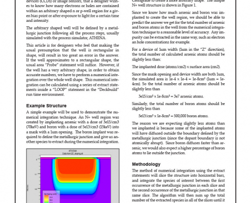 https://silvaco.com/wp-content/uploads/2020/03/simstd_Q2_2011_a2.jpg
1012
782
Ingrid Schwarz
/wp-content/uploads/2019/11/silvaco-logo.png
Ingrid Schwarz2011-04-01 16:49:022020-12-19 11:55:37Extracting Concentrations from Arbitrary Shaped Well Regions
https://silvaco.com/wp-content/uploads/2020/03/simstd_Q2_2011_a2.jpg
1012
782
Ingrid Schwarz
/wp-content/uploads/2019/11/silvaco-logo.png
Ingrid Schwarz2011-04-01 16:49:022020-12-19 11:55:37Extracting Concentrations from Arbitrary Shaped Well Regions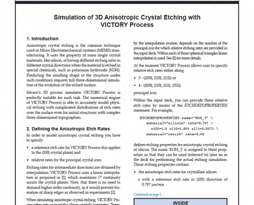 https://silvaco.com/wp-content/uploads/2020/03/simstd_Q2_2011_a1.jpg
1012
782
Ingrid Schwarz
/wp-content/uploads/2019/11/silvaco-logo.png
Ingrid Schwarz2011-04-01 16:44:232020-12-22 11:24:22Simulation of 3D Anisotropic Crystal Etching with VICTORY Process
https://silvaco.com/wp-content/uploads/2020/03/simstd_Q2_2011_a1.jpg
1012
782
Ingrid Schwarz
/wp-content/uploads/2019/11/silvaco-logo.png
Ingrid Schwarz2011-04-01 16:44:232020-12-22 11:24:22Simulation of 3D Anisotropic Crystal Etching with VICTORY Process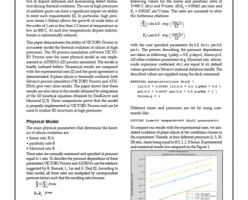 https://silvaco.com/wp-content/uploads/2020/03/simstd_Q1_2011_a3.jpg
1012
782
Ingrid Schwarz
/wp-content/uploads/2019/11/silvaco-logo.png
Ingrid Schwarz2011-02-01 16:30:282020-08-11 19:42:13Using VICTORY Process to Simulate Thermal Oxidation of Silicon at High Pressures of Ambient Gases
https://silvaco.com/wp-content/uploads/2020/03/simstd_Q1_2011_a3.jpg
1012
782
Ingrid Schwarz
/wp-content/uploads/2019/11/silvaco-logo.png
Ingrid Schwarz2011-02-01 16:30:282020-08-11 19:42:13Using VICTORY Process to Simulate Thermal Oxidation of Silicon at High Pressures of Ambient Gases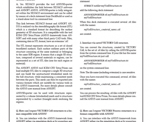 https://silvaco.com/wp-content/uploads/2020/03/simstd_Q1_2011_hints.jpg
1012
782
Ingrid Schwarz
/wp-content/uploads/2019/11/silvaco-logo.png
Ingrid Schwarz2011-01-01 16:32:532020-12-22 16:48:16Hints, Tips, and Solutions – Export 3D Structures from VICTORY Cell/Process to ANSOFT ANSYS
https://silvaco.com/wp-content/uploads/2020/03/simstd_Q1_2011_hints.jpg
1012
782
Ingrid Schwarz
/wp-content/uploads/2019/11/silvaco-logo.png
Ingrid Schwarz2011-01-01 16:32:532020-12-22 16:48:16Hints, Tips, and Solutions – Export 3D Structures from VICTORY Cell/Process to ANSOFT ANSYS https://silvaco.com/wp-content/uploads/2020/03/simstd_Q1_2011_a2.jpg
1012
782
Ingrid Schwarz
/wp-content/uploads/2019/11/silvaco-logo.png
Ingrid Schwarz2011-01-01 16:27:472020-12-22 10:18:49The Doping Effect Simulation on the OLED Devices Using ATLAS
https://silvaco.com/wp-content/uploads/2020/03/simstd_Q1_2011_a2.jpg
1012
782
Ingrid Schwarz
/wp-content/uploads/2019/11/silvaco-logo.png
Ingrid Schwarz2011-01-01 16:27:472020-12-22 10:18:49The Doping Effect Simulation on the OLED Devices Using ATLAS https://silvaco.com/wp-content/uploads/2020/03/simstd_Q1_2011_a1.jpg
1012
782
Ingrid Schwarz
/wp-content/uploads/2019/11/silvaco-logo.png
Ingrid Schwarz2011-01-01 16:24:142020-12-21 12:49:56Design Consideration & Performance Analysis of MCT Based Dual Band (MWIR/LWIR) Photodetector
https://silvaco.com/wp-content/uploads/2020/03/simstd_Q1_2011_a1.jpg
1012
782
Ingrid Schwarz
/wp-content/uploads/2019/11/silvaco-logo.png
Ingrid Schwarz2011-01-01 16:24:142020-12-21 12:49:56Design Consideration & Performance Analysis of MCT Based Dual Band (MWIR/LWIR) Photodetector