How to Mesh in 2D TCAD
Introduction
Meshing for process in ATHENA or electrical characterisation in ATLAS is one of the biggest challenges that a user faces. Poor meshing in both ATHENA and ATLAS can lead to simulation failures. Poor meshing can also lead to inaccurate electrical results, which is potentially even worse. The effect that the mesh can have on the electrical results has been illustrated in [1]. An optimum mesh will have a sufficient number of points to ensure accuracy yet it will not have an excessive number of points as this will lead to an increase in simulation time.
For a more fundamental discussion on meshing in ATHENA an excellent article can be found in [2]. Further information on base mesh definition in ATHENA can be found in [3].
In this article a more applied approach is considered with discussion given to a selection of mesh enhancement techniques and situations the user might face. A very simple structure is used throughout this article to highlight these techniques.
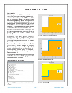
The deck used to create the basic structure used in this article is shown in Figure 1a. Images of the structure at key processing steps are shown in Figures 1b – e. Firstly, a trench region is etched from the silicon (Figure 1b), a liner oxide is then deposited (Figure 1c), followed by a poly trench re-fill (Figure 1d), finally the poly silicon is cleaned off (Figure 1e).
Please note that extremes and simplifications have been used in this article so as to clearly highlight and introduce a basic range of techniques.


