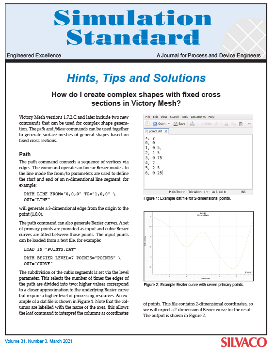
Victory Mesh versions 1.7.2.C and later include two new commands that can be used for complex shape genera-tion. The path and follow commands can be used together to generate surface meshes of general shapes based on fixed cross sections.
PathThe path command connects a sequence of vertices via edges. The command operates in line or Bezier modes. In the line mode the from/to parameters are used to define the start and end of an n-dimensional line segment, for example:
https://silvaco.com/wp-content/uploads/2021/03/Q1_SS_Mar2021-1.png724567Erick Castellon/wp-content/uploads/2019/11/silvaco-logo.pngErick Castellon2021-03-04 16:21:142021-03-04 17:24:37How do I create complex shapes with fixed cross sections in Victory Mesh?
We detect a local maximum in the design space of a pseudomorphic-channel high electron mobility transistor (PHEMT). The design has an OIP3 linearity figure-of-merit that is 10-15 dBm above the baseline for a similar 1 mm width control device, and is achieved at a gate bias on the order of 100 mA/mm or less, where the ratio of transconductance to the bias current gm1/ID is particularly large (7 volt-1).
https://silvaco.com/wp-content/uploads/2021/02/simstd_feb_2021_a1.jpg600470Erick Castellon/wp-content/uploads/2019/11/silvaco-logo.pngErick Castellon2021-02-03 19:16:132021-03-04 17:26:02Parabolic Grading of a PHEMT Channel Composition for Ultra-High and Broad OIP3 Peak
Gallium Nitride (GaN) based devices such as the High Electron Mobility Transistors (HEMTs) find wide applications in RF and Power domain due to its excellent intrinsic properties. Accordingly, such devices have also been explored for their radiation hardness which is inherent due to the strong bonding nature of the binary and ternary nitrides. Radiation-induced instabilities including the radiation-induced stress and changes to the material properties leading to the departure of expected results in practical applications. Due to the limited availability of the test structures and facilities required to analyze the reliability of said devices under ionizing radiations, the cost and time of production gets affected. In this regard, to cut down on the cost and time for production, device engineers require accurate and reliable tools that can accurately predict the robustness of their proposed device architectures in foreign environments. Silvaco’s Victory TCAD software is one such tool that can aid the device engineers in this aspect. In this work, we demonstrate the Total Ionizing Dose (TID) Effects on GaN HEMTs using the Radiation Effects Module (REM) available with Silvaco’s Victory TCAD suite.
https://silvaco.com/wp-content/uploads/2021/01/simstd_jan_2021_a1.png875668Graham Bell/wp-content/uploads/2019/11/silvaco-logo.pngGraham Bell2021-01-04 12:04:432021-01-11 17:21:14TCAD Investigation of Total Ionizing Dose (TID) Effects on Gallium Nitride HEMTs
In the simulation standard article, “Plasmonic Light Trapping Transforming Thin-Film Photovoltaics” from 2015, the finite difference time domain (FDTD) algorithm was used in 2D to propagate the light in thin film photovoltaic structures with and without metallic nanoparticles to simulate its plasmonic effect. The solid modeling module of Victory Mesh offers the capability to model such structures in 3D.
https://silvaco.com/wp-content/uploads/2020/12/simstd_dec_2020_a4.png909703Graham Bell/wp-content/uploads/2019/11/silvaco-logo.pngGraham Bell2020-12-02 10:31:342020-12-24 16:17:32Obtaining Spectral Sweeps from 3D Plasmonic Structures
In this paper the critical design features of a SiC superjunction trench MOS device were optimized using CAD to obtain a high breakdown voltage while minimizing any unnecessary increase in channel resistance.
https://silvaco.com/wp-content/uploads/2020/10/simstd_Q3_2020_a1.jpg724567Erick Castellon/wp-content/uploads/2019/11/silvaco-logo.pngErick Castellon2020-10-01 00:05:322020-10-05 18:04:17Optimizing a 2um, 1,500 Volt SiC Superjunction Trench-MOS Device Using TCAD
Conductive Bridge Random Access Memory (CBRAM) is a non-volatile memory device technology that can operate by consuming very low power. Another advantage of the CBRAM devices is its ability to be easily integrated into conventional back-end-of-line CMOS processes [1].
https://silvaco.com/wp-content/uploads/2020/10/simstd_Q3_2020_a2.jpg719546Erick Castellon/wp-content/uploads/2019/11/silvaco-logo.pngErick Castellon2020-10-01 00:04:372020-10-05 18:04:52TCAD Simulation of CBRAM Devices
Silvaco uses cookies to improve your user experience and to provide you with content we believe will be of interest to you. Learn detailed information on Privacy Policy. By using this website, you consent to the use of our cookies.
We may request cookies to be set on your device. We use cookies to let us know when you visit our websites, how you interact with us, to enrich your user experience, and to customize your relationship with our website.
Click on the different category headings to find out more. You can also change some of your preferences. Note that blocking some types of cookies may impact your experience on our websites and the services we are able to offer.
Essential Website Cookies
These cookies are strictly necessary to provide you with services available through our website and to use some of its features.
Because these cookies are strictly necessary to deliver the website, refuseing them will have impact how our site functions. You always can block or delete cookies by changing your browser settings and force blocking all cookies on this website. But this will always prompt you to accept/refuse cookies when revisiting our site.
We fully respect if you want to refuse cookies but to avoid asking you again and again kindly allow us to store a cookie for that. You are free to opt out any time or opt in for other cookies to get a better experience. If you refuse cookies we will remove all set cookies in our domain.
We provide you with a list of stored cookies on your computer in our domain so you can check what we stored. Due to security reasons we are not able to show or modify cookies from other domains. You can check these in your browser security settings.
Google Analytics Cookies
These cookies collect information that is used either in aggregate form to help us understand how our website is being used or how effective our marketing campaigns are, or to help us customize our website and application for you in order to enhance your experience.
If you do not want that we track your visit to our site you can disable tracking in your browser here:
Other external services
We also use different external services like Google Webfonts, Google Maps, and external Video providers. Since these providers may collect personal data like your IP address we allow you to block them here. Please be aware that this might heavily reduce the functionality and appearance of our site. Changes will take effect once you reload the page.
Google Webfont Settings:
Google Map Settings:
Google reCaptcha Settings:
Vimeo and Youtube video embeds:
Other cookies
The following cookies are also needed - You can choose if you want to allow them:
Privacy Policy
You can read about our cookies and privacy settings in detail on our Privacy Policy Page.

 https://silvaco.com/wp-content/uploads/2021/03/Q1_SS_Mar2021-1.png
724
567
Erick Castellon
/wp-content/uploads/2019/11/silvaco-logo.png
Erick Castellon2021-03-04 16:21:142021-03-04 17:24:37How do I create complex shapes with fixed cross sections in Victory Mesh?
https://silvaco.com/wp-content/uploads/2021/03/Q1_SS_Mar2021-1.png
724
567
Erick Castellon
/wp-content/uploads/2019/11/silvaco-logo.png
Erick Castellon2021-03-04 16:21:142021-03-04 17:24:37How do I create complex shapes with fixed cross sections in Victory Mesh?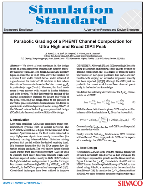 https://silvaco.com/wp-content/uploads/2021/02/simstd_feb_2021_a1.jpg
600
470
Erick Castellon
/wp-content/uploads/2019/11/silvaco-logo.png
Erick Castellon2021-02-03 19:16:132021-03-04 17:26:02Parabolic Grading of a PHEMT Channel Composition for Ultra-High and Broad OIP3 Peak
https://silvaco.com/wp-content/uploads/2021/02/simstd_feb_2021_a1.jpg
600
470
Erick Castellon
/wp-content/uploads/2019/11/silvaco-logo.png
Erick Castellon2021-02-03 19:16:132021-03-04 17:26:02Parabolic Grading of a PHEMT Channel Composition for Ultra-High and Broad OIP3 Peak https://silvaco.com/wp-content/uploads/2021/01/simstd_jan_2021_a1.png
875
668
Graham Bell
/wp-content/uploads/2019/11/silvaco-logo.png
Graham Bell2021-01-04 12:04:432021-01-11 17:21:14TCAD Investigation of Total Ionizing Dose (TID) Effects on Gallium Nitride HEMTs
https://silvaco.com/wp-content/uploads/2021/01/simstd_jan_2021_a1.png
875
668
Graham Bell
/wp-content/uploads/2019/11/silvaco-logo.png
Graham Bell2021-01-04 12:04:432021-01-11 17:21:14TCAD Investigation of Total Ionizing Dose (TID) Effects on Gallium Nitride HEMTs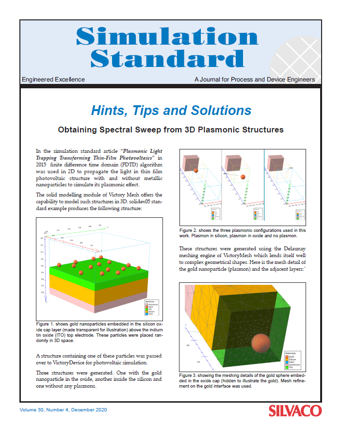 https://silvaco.com/wp-content/uploads/2020/12/simstd_dec_2020_a4.png
909
703
Graham Bell
/wp-content/uploads/2019/11/silvaco-logo.png
Graham Bell2020-12-02 10:31:342020-12-24 16:17:32Obtaining Spectral Sweeps from 3D Plasmonic Structures
https://silvaco.com/wp-content/uploads/2020/12/simstd_dec_2020_a4.png
909
703
Graham Bell
/wp-content/uploads/2019/11/silvaco-logo.png
Graham Bell2020-12-02 10:31:342020-12-24 16:17:32Obtaining Spectral Sweeps from 3D Plasmonic Structures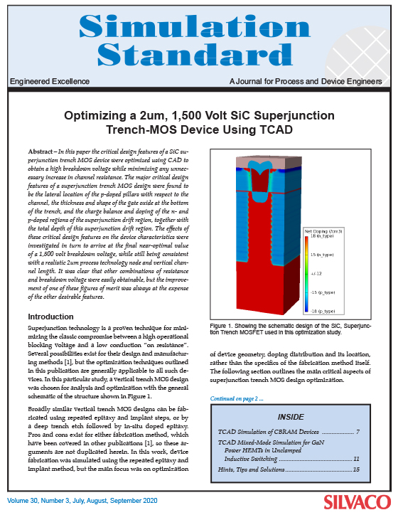 https://silvaco.com/wp-content/uploads/2020/10/simstd_Q3_2020_a1.jpg
724
567
Erick Castellon
/wp-content/uploads/2019/11/silvaco-logo.png
Erick Castellon2020-10-01 00:05:322020-10-05 18:04:17Optimizing a 2um, 1,500 Volt SiC Superjunction Trench-MOS Device Using TCAD
https://silvaco.com/wp-content/uploads/2020/10/simstd_Q3_2020_a1.jpg
724
567
Erick Castellon
/wp-content/uploads/2019/11/silvaco-logo.png
Erick Castellon2020-10-01 00:05:322020-10-05 18:04:17Optimizing a 2um, 1,500 Volt SiC Superjunction Trench-MOS Device Using TCAD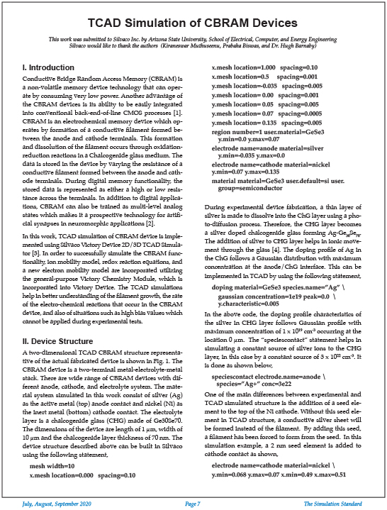 https://silvaco.com/wp-content/uploads/2020/10/simstd_Q3_2020_a2.jpg
719
546
Erick Castellon
/wp-content/uploads/2019/11/silvaco-logo.png
Erick Castellon2020-10-01 00:04:372020-10-05 18:04:52TCAD Simulation of CBRAM Devices
https://silvaco.com/wp-content/uploads/2020/10/simstd_Q3_2020_a2.jpg
719
546
Erick Castellon
/wp-content/uploads/2019/11/silvaco-logo.png
Erick Castellon2020-10-01 00:04:372020-10-05 18:04:52TCAD Simulation of CBRAM Devices