Simulation Standard Technical Journal
A Journal for Process and Device Engineers
Calibration of the Ion Enhanced Chemical Etching Model of VICTORY Process Using Virtual Wafer Fab
In this article we describe a technique to automatically calibrate parameters of an Ion Enhanced Chemical Etching model implemented in the 3D process simulator VICTORY Process to measurements published in [1]. We will briefly describe the model and show how an experiment applying this model can be set up in VWF to automate the calibration by carrying out several individual simulations without user interaction.
Using VICTORY Process to Model the Effect of Silicon Substrate Orientation on Oxidation Kinetics
Different crystal planes of silicon are known to have different oxidation rates, e.g. the silicon plane with Miller indices <111> is oxidized approximately 1.7 times faster then the <100> plane [1][2]. During an oxidation process the geometry of a 3D structure may change significantly and the silicon/oxide interface may pass through various crystal planes with different oxidation rates. Therefore, the orientation and type of the silicon wafer affects the resulting geometry of an oxidized structure on this wafer. This paper explains in details how VICTORY Process can be used to model this anisotropic behaviour.
A Semi-Empirical Model for the Simulation of Ion Milling in VICTORY Process
The three-dimensional process simulator VICTORY Process now includes a semi-empirical model for the simulation of ion milling. During ion milling, the mill (etch) rate depends in a complex way on the local beam’s incidence angle (angle between beam direction and the normal at a particular surface point). The function describing this relationship is called the angle dependent mill rate. A visual representation of such an angle dependent mill rate is shown in Figure 1.
Developing Custom Etching/Deposition Models in VICTORY Process
VICTORY Process is supplied with a wide range of models and data for an extensive set of materials, so that you can simulate many process steps without the need to make changes in the default setup. However, you may wish to expand its capability by using your proprietary data and models. Thanks to the open modeling interface used by VICTORY Process
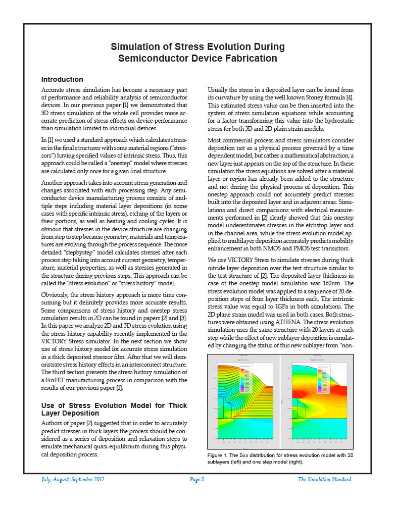
Simulation of Stress Evolution During Semiconductor Device Fabrication
Accurate stress simulation has become a necessary part of performance and reliability analysis of semiconductor devices. In our previous paper [1] we demonstrated that 3D stress simulation of the whole cell provides more accurate prediction of stress effects on device performance than simulation limited to individual devices.
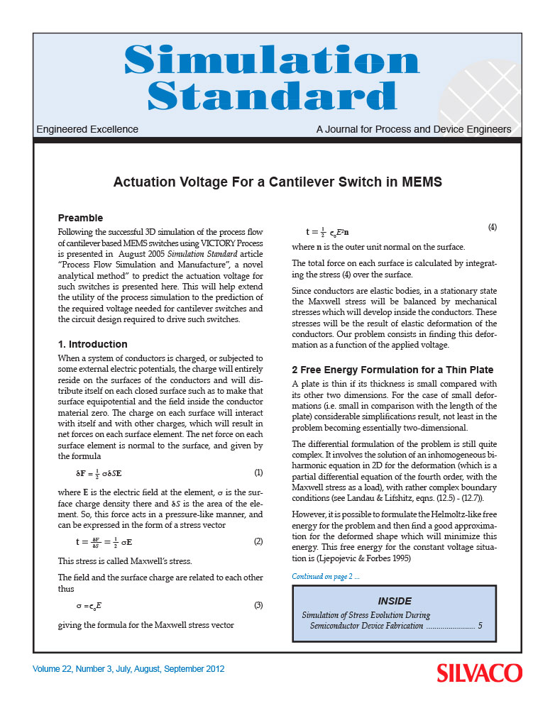
Actuation Voltage For a Cantilever Switch in MEMS
Following the successful 3D simulation of the process flow of cantilever based MEMS switches using VICTORY Process is presented in August 2005 Simulation Standard article “Process Flow Simulation and Manufacture”, a novel analytical method to predict the actuation voltage for such switches is presented here. This will help extend the utility of the process simulation to the prediction of the required voltage needed for cantilever switches and the circuit design required to drive such switches.

