Simulation Standard Technical Journal
A Journal for Process and Device Engineers

ZnO based LED: A Performance Optimization through TCAD Simulation
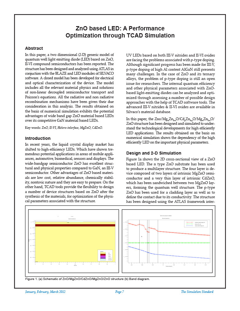
In this paper, a two dimensional (2-D) generic model of quantum well light emitting diode (LED) based on ZnO, II-VI compound semiconductors has been reported. The structure has been designed and analyzed using ATLAS in conjuction with the BLAZE and LED modules of SILVACO software. A closed model has been developed for electrical and optical characterization of the device. The model includes all the relevant material physics and solutions of non-linear decoupled semiconductor transport and Poisson’s equations. All the radiative and non radiative recombination mechanisms have been given their due consideration in this analysis. The results obtained on the basis of numerical simulation exhibits the potential advantages of wide band gap ZnO material based LEDs over its competitive GaN material based LEDs.

Normally-off AlGaN/GaN HFET with p-type GaN Gate and AlGaN Buffer
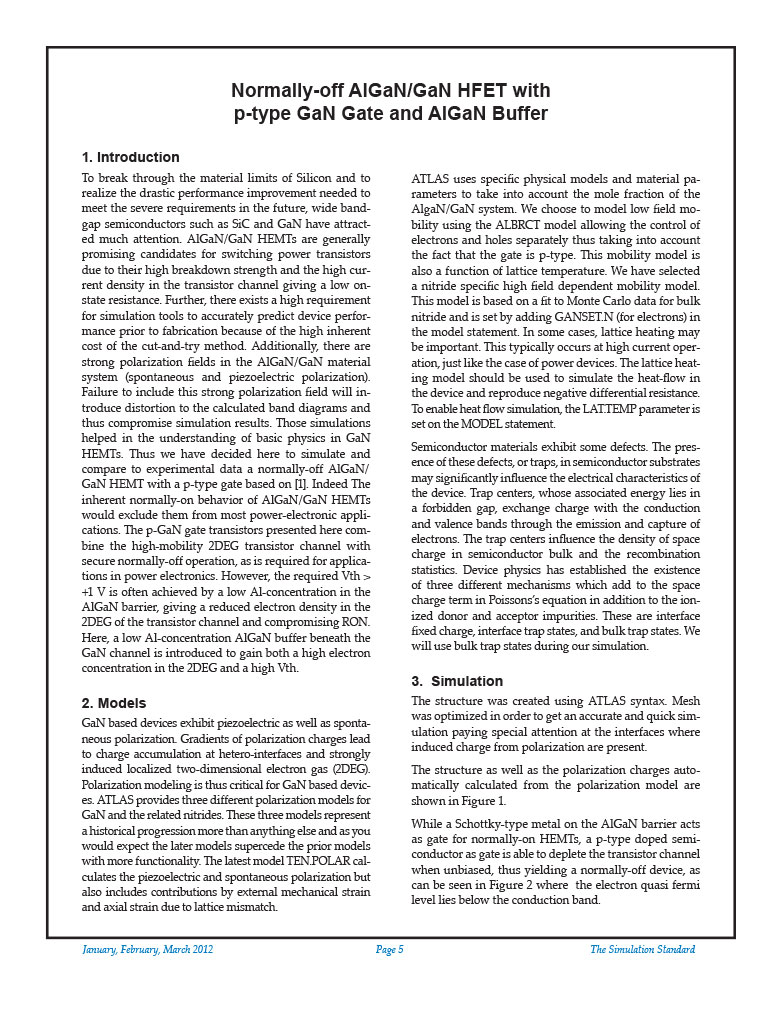
To break through the material limits of Silicon and to realize the drastic performance improvement needed to meet the severe requirements in the future, wide bandgap semiconductors such as SiC and GaN have attracted much attention. AlGaN/GaN HEMTs are generally promising candidates for switching power transistors due to their high breakdown strength and the high current density in the transistor channel giving a low on-state resistance. Further, there exists a high requirement for simulation tools to accurately predict device performance prior to fabrication because of the high inherent cost of the cut-and-try method.

Simulation of Stresses and Mobility Enhancement Factors in 3D Inverter Cell
The analysis and characterization of stress effects have become an integral part of semiconductor technology and device design. In a typical semiconductor process flow the stresses are generated primarily due to volume expansion or contraction of the adjacent materials during temperature variations. Stresses could also be generated during oxidation, silicidation, etching, and deposition processes or due to lattice expansion or contraction after introducing large doses of dopants. Simulation of process induced stresses is an important component of traditional TCAD analysis since these stresses could have adverse or positive effect on individual process steps or on final device characteristics.

High Light Extraction on OLED with Microcavity Effects
OLEDs have been researched for application in display devices due to their considerable advantages. In order to further improve and optimize devices for practical applications, the electrical and optical parts have to be considered.

Modelling of GaN/InGaN Tricolour Multiple Quantum Well Light Emitting Diodes
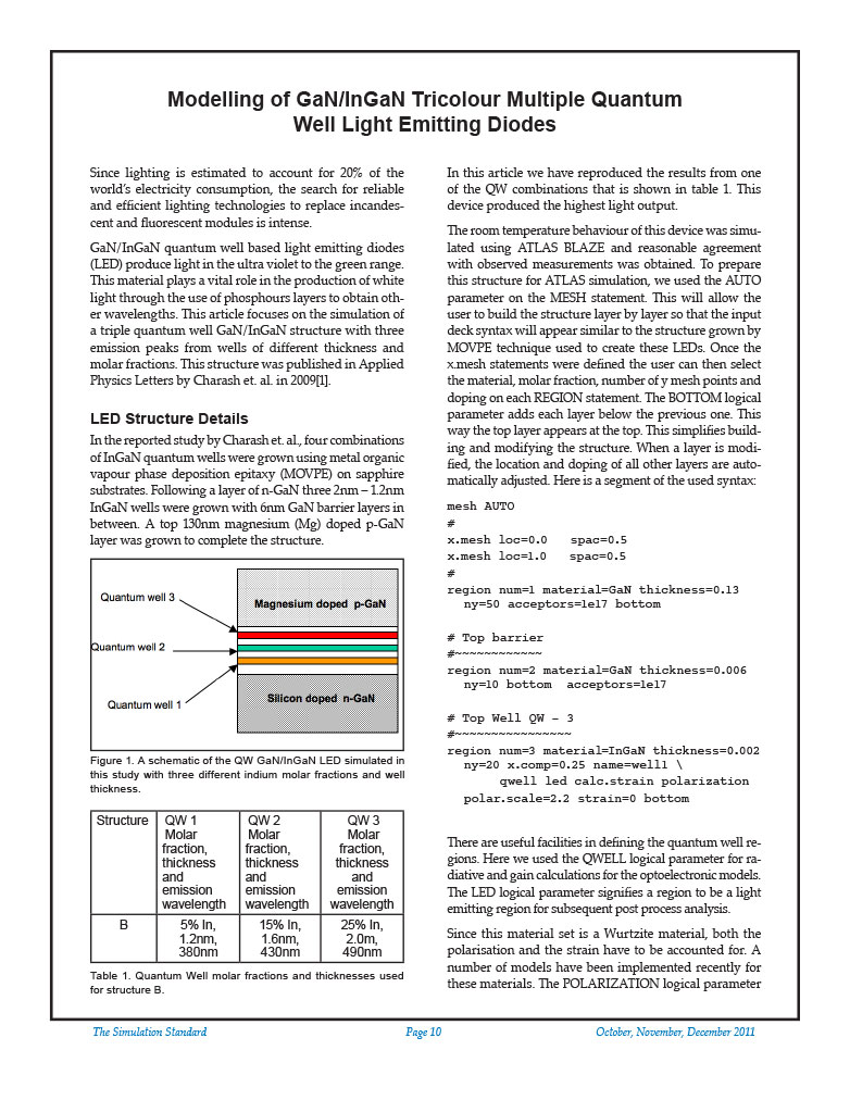
Since lighting is estimated to account for 20% of the world’s electricity consumption, the search for reliable and efficient lighting technologies to replace incandescent and fluorescent modules is intense.

InGaN/GaN Ridge Type with MQW Laser Diode Simulation Using ATLAS
The light source on short wavelenghts has been researched in GaN-based lser diodes (LDs). For high efficiency emitting devices, the wave-guide layer has been investigated to obtain more stable far field patterns and the multi-quantum well layers have been researched as a means of acheiving high quantum efficiency in blue-violet lasers.

