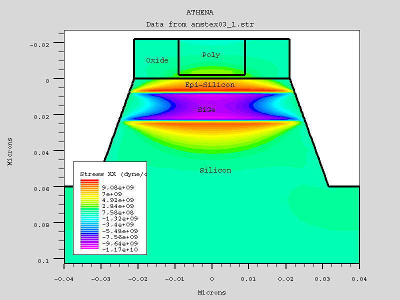
vwfex01 : Stress in MOSFET with Embedded SiGe Layer
Requires: VWF, ATHENA,
This example demonstrates simulation of stresses in a test MOSFET structure with an embedded SiGe layer. All important geometrical characterisics of the test structure, including thicknesses of different layers, spacer width, gate length, etc., are parametrized. This allows us to investigate the effects of parameter variations on important device characteristics using Virtual Wafer Fab (VWF).
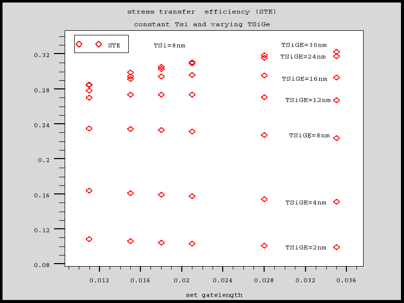
The important factor is the stress transfer efficiency (STE), specified as an absolute value of the ratio between the average stresses under the gate and initial stress in the SiGe buried layer.
Figs. 2, 3 and 4 of the following reference J.G. Fiorenza, et.al. "Detailed Simulation Study of a Reverse Embedded-SiGe Strained-Silicon MOSFET", IEEE Trans. on Electron Devices, v.55, No.2, p. 640, (2008). are shown.
To open and run this example, select the Help Load example button in the VWF explorer. This will import all examples into your database. Once imported, the examples will be available under the directory called examples.