opt_ex16 : HiSIM2 MOSFET Model Extraction
Requires: Utmost IV, SmartSpice, SmartView
Minimum Versions: Utmost IV 1.11.2.R, SmartSpice 4.16.1.R, SmartView 2.30.3.R
This example describes how to extract a standard HiSIM2 model. To extract a model which is scalable with geometry, multiple different device sizes must be included. In this example, twelve different geometry devices for DC and two geometry devices for capacitance at room temperature are included.
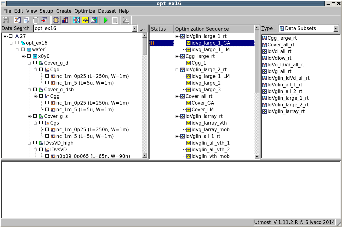
The project file opt_ex16.prj and the data file opt_ex16.uds for this example should be loaded into your database. When opened, the project will look as shown in opt_ex16_project.png .
The optimization sequence, which automates the parameter extraction, is divided into twelve sections. Some model parameters are optimized in multiple sections for better fitting.
Before starting the optimization sequence, the following process parameters are defined in the model library. The oxide thickness, tox, is set at this point. The other parameter values are used as starting values for further optimization during the sequence.
- tox:Physical oxide thickness
- nsubc:Substrate-impurity concentration
- nsubp:Maximum pocket concentration
- lover:Overlap length
- nover:Impurity concentration in overlap region
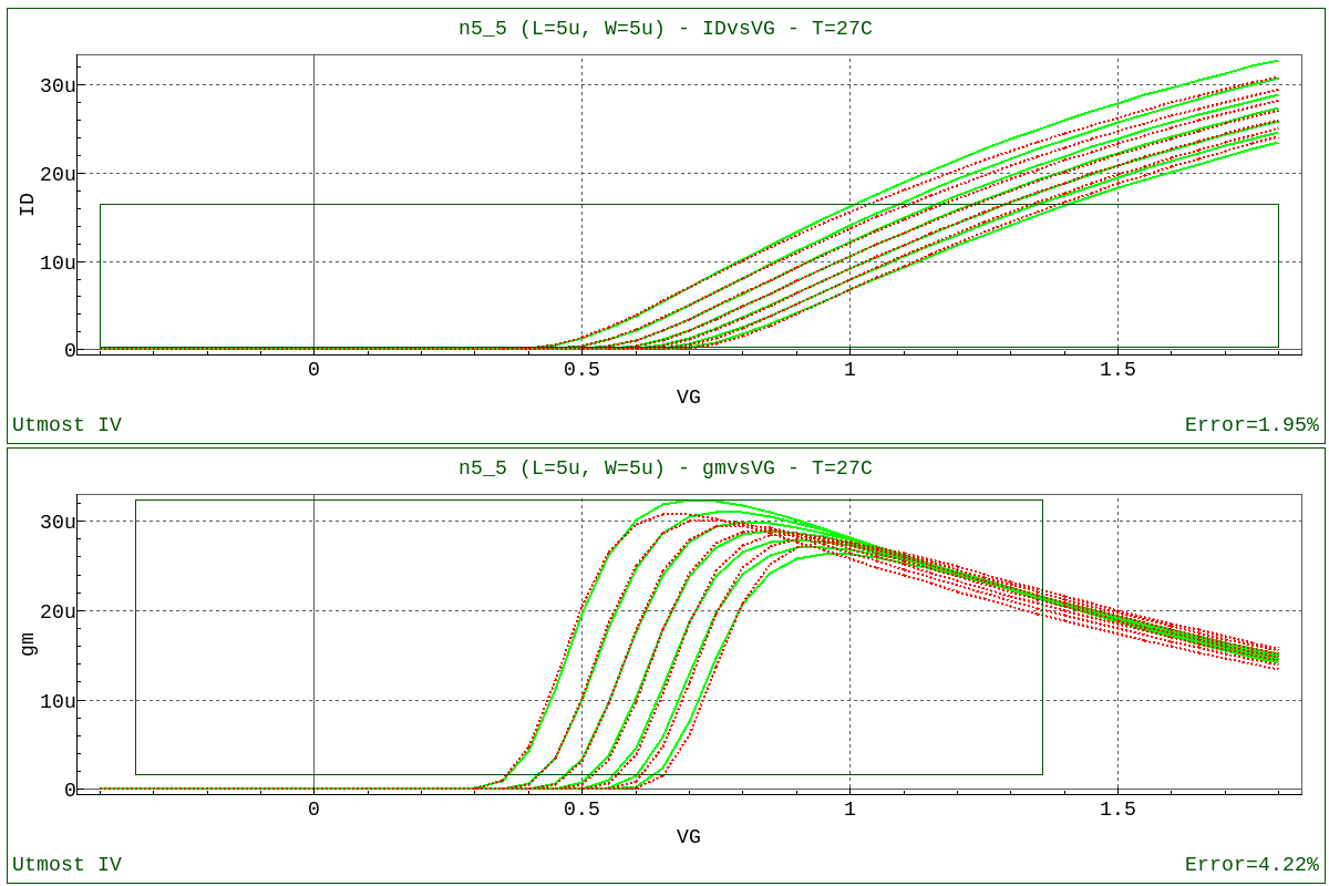
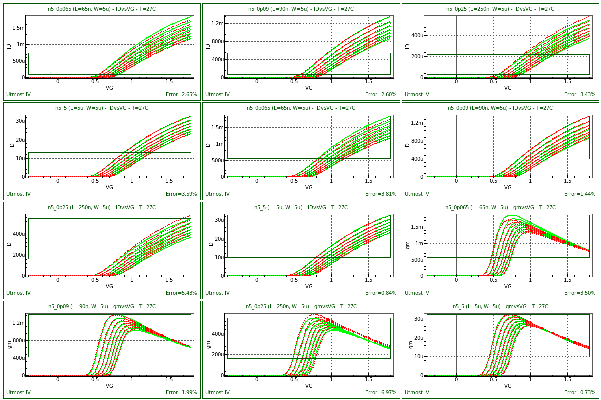
Section 1 : IdVglin_large_1_rt
This section optimizes the parameters for linear gate turn on characteristics at large size device. The data is the drain current vs. gate voltage characteristics at low drain voltage (IDvsVG_lin). This section has two steps. The first step uses the Genetic Algorithm(GA) optimizer and the second step uses the Levenberg-Marquardt Algorithm(LM) optimizer. The following parameters are optimized;
- nsubc:Substrate-impurity concentration
- vfbc:Flat-band voltage
- ndep:Depletion charge contribution on effective-electric field
- muecb0:Coulomb scattering
- muecb1:Coulomb scattering
- mueph0:Phonon scattering
- mueph1:Phonon scattering
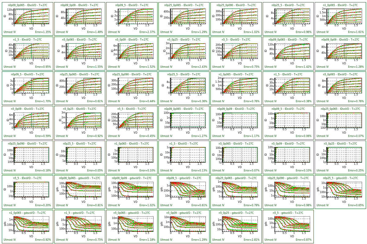
After this section is completed, the fit to measured data is as shown in opt_ex16_01.png .
Section 2 : Cgg_large_rt
This section optimizes the parameters for total gate capacitance (Cgg) characteristics. The data is Cgg and algorithm is LM. The following parameters are optimized;
- lover:Overlap length
- vfbover:Flat-band voltage in overlap region
- pgd1:Strength of poly-depletion effect
- pgd2:Threshold voltage of poly-depletion effect
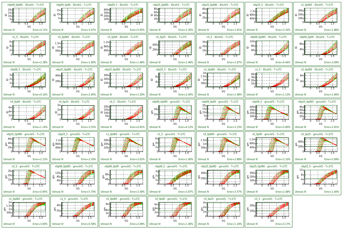
After this section is completed, the fit to measured data is shown in opt_ex16_02.png .
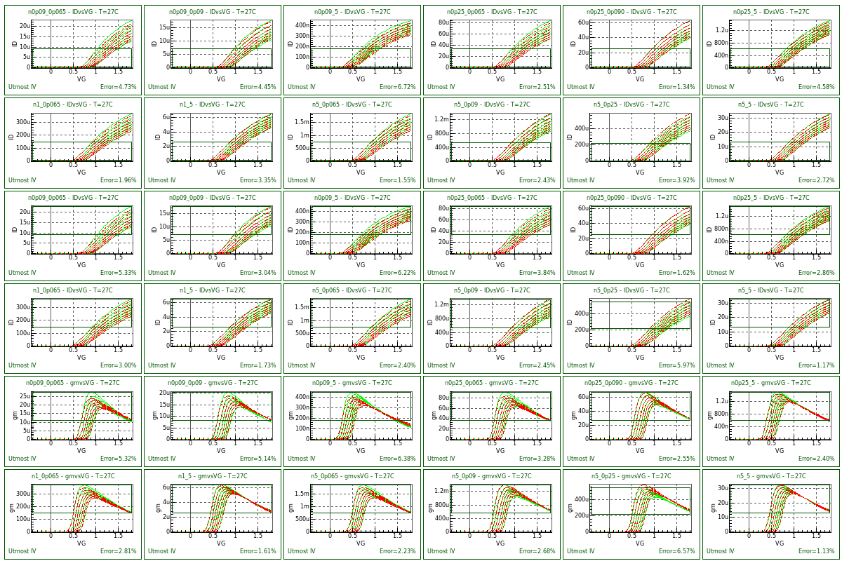
Section 3 : IdVglin_large_2_rt
This section optimizes the parameters for threshold, mobility and resistance characteristics at large size device. This section has three steps and all steps use LM. The following parameters are optimized;
- muesr0:Surface-roughness scattering
- muesr1:Surface-roughness scattering
- ninv:Inversion charge contribution on effective-electric field
The following model parameters, which have already been optimized previously, are again optimized to ensure the fit to the entire data.
- nsubc
- vfbc
- ndep
- muecb0
- muecb1
- mueph0
- mueph1
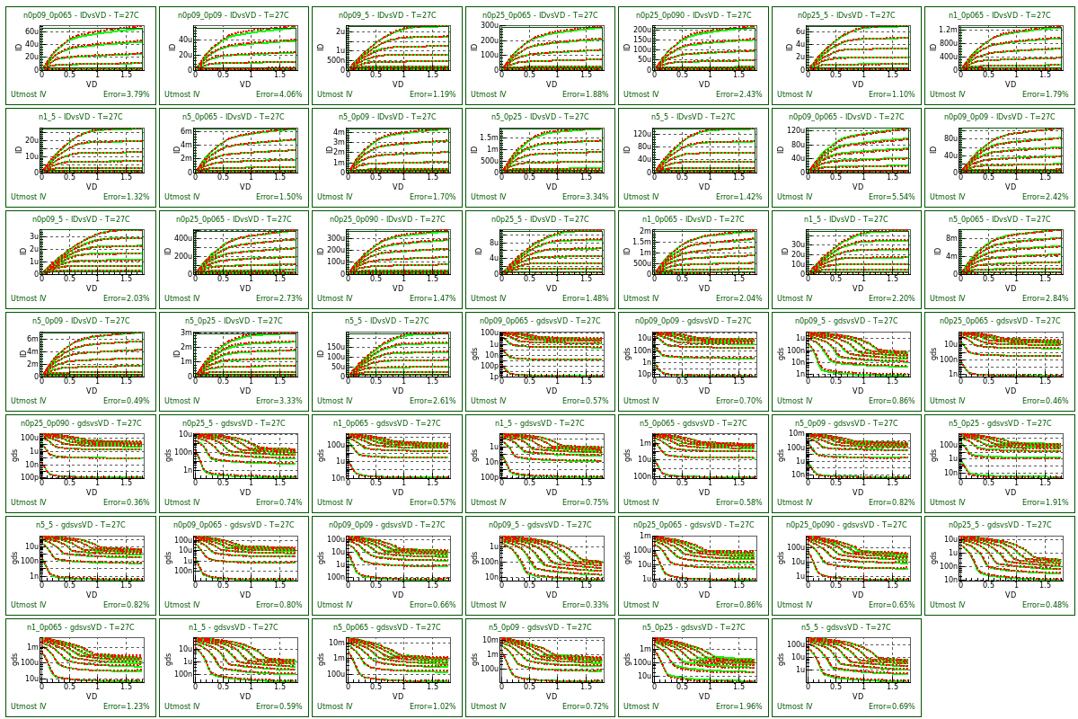
After this section is completed, the fit to measured data is shown in opt_ex16_03.png .
Section 4 : Cover_all_rt
This section optimizes the parameters for overlap capacitance characteristics. This uses the Cgg, Cgd and Cgs data. This section has two steps, the first step uses GA and the second step uses LM. The following parameters are optimized;
- xld:Gate-overlap length
- xwd:Gate-overlap width
- nover:Impurity concentration in overlap region
- pgd4:L dependence of poly-depletion effect
- cgdo:Gate-to-drain overlap capacitance
- cgso:Gate-to-source overlap capacitance
The following model parameters, which have already been optimized previously, are again optimized to ensure the fit to the entire data.
- lover
- vfbover
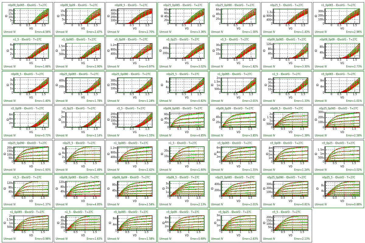
After this section is completed, the fit to measured data is shown in opt_ex16_04.png .
Section 5 : IdVglin_larray_rt
This section optimizes the parameters for threshold, mobility and resistance characteristics for devices with large width and various lengths. This section has two steps and all steps use LM. The following parameters are optimized;
- nsubp:Maximum pocket concentration
- lp:Pocket penetration length
- muephl:Length dependence of phonon mobility reduction
- muesrl:Length dependence of surface roughness mobility reduction
- ndepl:Modification of QB contribution for short-channel case
- parl2:Depletion width of channel/contact junction
- sc1:Magnitude of short-channel effect
- sc3:Vds dependence of short-channel effect
After this section is completed, the fit to measured data is shown in opt_ex16_05.png .
Section 6 : IdVglin_all_1_rt
This section optimizes the parameters for threshold, mobility and resistance characteristics for all device sizes. The data is IDvsVG_lin and this section has three steps, all of which use LM. The following parameters are optimized;
- muephs:Mobility modification due to small size
- muephw:Width dependence of phonon mobility reduction
- muepld:Length dependence of phonon mobility reduction
- muepwd:Width dependence of phonon mobility reduction
- muesrw:Change of surface roughness related mobility
- scp1:Magnitude of short-channel effect due to pocket
- scp3:Vds dependence of short-channel due to pocket
- wfc:Threshold voltage change due to capacitance change
- wl2:Threshold voltage shift due to small size effect
- wl2p:Threshold voltage shift due to small size effect
- wvth0:Threshold voltage shift
- ndepw:Modification of universal mobility for narrow width
- ndepwp:Modification of universal mobility for narrow width
The following model parameters, which have already been optimized previously, are again optimized to ensure the fit to the entire data.
- muephl
- muesrl
- ndep
- ndepl
- parl2
- ninv
- sc1
- sc3
- xld
- xwd
After this section is completed, the fit to measured data is shown in opt_ex16_06.png .
Section 7 : IdVglin_IdVd_all_rt
This section optimizes the parameters for threshold and low gate voltage region characteristics at all device sizes. The data is IDvsVG_lin and the drain current vs. drain voltage characteristics at low body voltage (IDvsVD_low), and this section has three steps. The first and third steps use LM, the second step uses GA. The following parameters are optimized;
- nsubcw:Modification of substrate concentration for narrow width
- nsbcwp:Modification of substrate concentration for narrow width
- nsubpl:Initial channel length of NSUBP reduction
- nsubpw:Modification of pocket concentration for narrow width
- nsubpwp:Modification of pocket concentration for narrow width
- clm1:Hardness coefficient of channel/contact junction
- clm2:Coefficient for QB contribution
- clm3:Coefficient for QI contribution
- clm5:Effect of pocket implantation
- clm6:Effect of pocket implantation
- gidl1:Magnitude of GIDL
- gidl2:Field dependence of GIDL
- gidl3:Vds dependence of GIDL
- gidl4:Threshold of Vds dependence
- gidl5:Correction of high-field contribution
- gidl6:Threshold of Vbs dependence
- gidl7:Correction of high-field contribution
- glksd1:Gate to source/drain current coefficient
- sc2:Vds dependence of short-channel effect
- scp2:Vds dependence of short-channel due to pocket
- sc4:Coupling of Vds-Vbs dependence
- sub1:Substrate current coefficient of magnitude
- sub1l:Lgate dependence SUB1
- sub2:Substrate current coefficient of exponential term
- svbs:Substrate current dependence on Vbs
- svgs:Substrate current dependence on Vgs
- svgsl:L dependence of SVGS
- svgsw:W dependence of SVGS
The following model parameters, which have already been optimized previously, are again optimized to ensure the fit to the entire data.
- nsubp
- parl2
- sc1
- sc3
- scp1
- scp3
- wfc
- wl2
- wl2p
- wvth0
After this section is completed, the fit to measured data is shown in opt_ex16_07.png .
Section 8 : IdVglin_all_2_rt
The purpose of this section is to tune the parameters that were optimized in the previous sections. This section optimizes the parameters for the linear region characteristics at all device sizes. This section has three steps and all steps use LM. The following parameters are re-optimized;
- mueph0
- mueph1
- muesr0
- muesr1
- muephl
- muephs
- muephw
- muepld
- muepwd
- muesrl
- muesrw
- nsubcw
- ndep
- ndepl
- ndepw
- ndepwp
- ninv
- sc1
- sc3
- scp1
- scp3
- wfc
- wl2
- wl2p
- wvth0
After this section is completed, the fit to measured data is shown in opt_ex16_08.png .
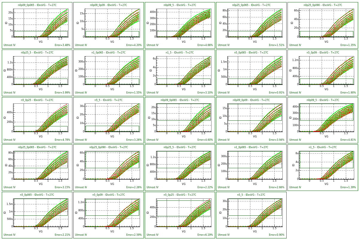
Section 9 : IdVdlow_rt
This section optimizes the parameters for saturation region characteristics at all device sizes. The data is IDvsVD_low. This section has three steps and all steps use LM. The following parameters are optimized;
- ninvd:Reduced resistance effect for small Vds
- mueslp:Length dependence of surface roughness mobility reduction
- mueswp:Change of surface roughness related mobility
- muepsp:Mobility modification due to small size
- vmax:Saturation velocity
- vover:Velocity overshoot effect
- voverp:Leff dependence of velocity overshoot
- vovers:Modification of maximum velocity due to small size
- voversp:Modification of maximum velocity due to small size
- svds:Substrate current dependence on Vds
- sub2l:L dependence of SUB2
- ndeplp:Modification of QB contribution for short-channel case
- ndepw:Modification of universal mobility for narrow width
- ndepwp:Modification of universal mobility for narrow width
The following model parameters, which have already been optimized previously, are again optimized to ensure the fit to the entire data.
- clm1
- clm2
- clm3
- clm5
- clm6
- muesr0
- muesr1
- muesrl
- muesrw
- muephs
- wvth0
- ninv
- wl2
- wl2p
- ndep
- ndepl
- sc2
- scp2
- sub1
- sub1l
- sub2
- svgs
- svgsl
- pgd1
- pgd2
- pgd4
After this section is completed, the fit to measured data is shown in opt_ex16_09.png .
Section 10 : IdVg_all_rt
This section optimizes the parameters for linear and saturation region characteristics at all device sizes. The data used are IDvsVG_lin and the drain current vs. gate voltage characteristics at high drain voltage (IDvsVG_sat) This section has one step which uses LM. The following parameters are optimized;
- sc3vbs:For diminishing of impunity gradient
- sc4:Coupling of Vds-Vbs dependence
- bs1:Body-coefficient modification by impurity profile
- bs2:Body-coefficient modification by impurity profile
- bb:High-field-mobility degradation
- svbs:Substrate current dependence on Vbs
- svbsl:Lgate dependence of SVBS
- svbslp:Lgate dependence of SVBS
The following model parameters, which have already been optimized previously, are again optimized to ensure the fit to the entire data.
- muephl
- muephs
- muephw
- muepld
- muepwd
- muesrl
- muesrw
- ndep
- ndepl
- ndepw
- ndepwp
- ninv
- sc1
- sc2
- sc3
- scp1
- scp3
- wfc
- wl2
- wl2p
- wvth0
After this section is completed, the fit to measured data is shown in opt_ex16_10.png .
Section 11 : IdVd_all_rt
This section optimizes the parameters for low and high body voltage characteristics at all device sizes. The data used are IDvsVD_low and the drain current vs. drain voltage characteristics at high body voltage (IDvsVD_high). This section has one step which uses LM. The following parameters are optimized;
- clm1
- clm2
- clm3
- clm5
- clm6
- wvth0
- ninv
- ninvd
- wl2
- wl2p
- ndep
- ndepl
- ndeplp
- ndepw
- ndepwp
- vmax
- vover
- voverp
- vovers
- voversp
- bs1
- bs2
- bb
- svbs
- svbsl
- svbslp
- pgd1
- pgd2
- pgd4
After this section is completed, the fit to measured data is shown in opt_ex16_11.png .
Section 12 : IdVg_IdVd_all_rt
The final section is for all geometry devices for the improvement of the entire fitting. All of the DC data is used, and the optimizer algorithm is LM. The following parameters are optimized;
- nsubc
- nsubp
- vfbc
- ndep
- muesr0
- muesr1
- muesrl
- muesrw
- sc1
- sc3
- sc4
- wfc
- wl2
- wl2p
- wvth0
- ninv
- ninvd
- mueslp
- mueswp
- vmax
- vover
- voverp
- vovers
- voversp
- bb
After this section is completed, the fit to measured data is shown in opt_ex16_12.png .
When the sequence is completed, the final model card can be exported into an external model library file as shown in opt_ex16.lib.
opt_ex16.lib
											.MODEL hisim2 NMOS (
+level    = 68             version  = '2.80'         corsrd   = 0
+corg     = 0              coiprv   = 1              copprv   = 1
+coadov   = 1              coisub   = 1              coiigs   = 1
+cogidl   = 1              coovlp   = 1              coflick  = 0
+coisti   = 1              conqs    = 0              cothrml  = 0
+coign    = 0              codfm    = 0              corbnet  = 0
+corecip  = 1              coqy     = 0              coqovsm  = 1
+codep    = 0              coddlt   = 0              bgtmp1   = 9.025e-05
+bgtmp2   = 1e-07          eg0      = 1.1785         tox      = 3e-09
+xld      = 0              lover    = 2.31277e-08    ddltmax  = 10
+ddltslp  = 0              ddltict  = 10             vfbover  = 0.175969
+nover    = 6.97345e+19    xwd      = 1.69796e-08    xl       = 0
+xw       = 0              saref    = 1e-06          sbref    = 1e-06
+ll       = 0              lld      = 0              lln      = 0
+wl       = 0              wl1      = 0              wl1p     = 1
+wl2      = -0.00140851    wl2p     = 1.09971        wld      = 0
+wln      = 0              web      = 0              wec      = 0
+rsh      = 0              rshg     = 0              xqy      = 1e-08
+xqy1     = 0              xqy2     = 2              qyrat    = 0.5
+rs       = 0              rd       = 0              vfbc     = -0.96247
+vfbcl    = 0              vfbclp   = 1              vbi      = 1.1
+nsubc    = 5.91496e+17    parl2    = 2.11778e-08    lp       = 8.48178e-09
+nsubp    = 9.48647e+18    nsubpl   = 0.001          nsubpfac = 1
+nsubpdlt = 0.01           nsubpw   = 0.000870403    nsubpwp  = 1.34001
+nsubpwpe = 0              scp1     = 0.811825       scp2     = 0
+scp3     = 9.41467e-10    sc1      = 5.93001        sc2      = 0
+sc3      = 0              sc4      = 0              sc3vbs   = -0.01
+pgd1     = 5.11888e-06    pgd2     = 0.3            pgd4     = 2.71656
+ndep     = 0.79632        ndepl    = 0.0199274      ndeplp   = 0.988503
+ndepw    = 0.00139971     ndepwp   = 1.43404        ninv     = 0.328159
+ninvd    = 0              muecb0   = 100            muecb0lp = 0
+muecb1   = 120.773        muecb1lp = 0              mueph0   = 0.31326
+mueph1   = 25751          muephw   = 0.01           muepwp   = 1
+muepwd   = 0              muephl   = -0.011291      mueplp   = 1
+muepld   = 1.1117e-09     muephs   = 0.00377578     muepsp   = 0.760251
+vtmp     = 0              wvth0    = 0.0184277      muesr0   = 2.01495
+muesr1   = 7.46963e+14    muesrl   = 0.00654517     muesrw   = 0.000389123
+mueswp   = 0.423638       mueslp   = 0.311361       muetmp   = 1.5
+bb       = 2.54647        sub1     = 0.00183906     sub2     = 10
+svgs     = 0.1            svbs     = 1              svbsl    = -5.82627e-07
+svds     = 1              slg      = 3e-08          sub1l    = 0.00185011
+sub2l    = 5.14366e-07    svgsl    = 0              svgslp   = 1
+svgswp   = 1              svgsw    = 0              svbslp   = 1.31121
+slgl     = 0              slglp    = 1              sub1lp   = 1
+nsti     = 5e+17          wsti     = 0              wstil    = 0
+wstilp   = 1              wstiw    = 0              wstiwp   = 1
+scsti1   = 0              scsti2   = 0              vthsti   = 0
+vdsti    = 0              muesti1  = 0              muesti2  = 0
+muesti3  = 1
+nsubpsti1 = 0
+nsubpsti2 = 0
+nsubpsti3 = 1
+lpext    = 1e-50          npext    = 8e+17          npextw   = 0
+npextwp  = 1              npextwpe = 0              scp21    = 0
+scp22    = 0              bs1      = 0              bs2      = 0.9
+tpoly    = 2e-07          cgbo     = 0              js0      = 5e-07
+js0sw    = 0              nj       = 1              njsw     = 1
+xti      = 2              cj       = 0.0005         cjsw     = 5e-10
+cjswg    = 5e-10          mj       = 0.5            mjsw     = 0.33
+mjswg    = 0.33           pb       = 1              pbsw     = 1
+pbswg    = 1              tcjbd    = 0              tcjbs    = 0
+tcjbdsw  = 0              tcjbssw  = 0              tcjbdswg = 0
+tcjbsswg = 0              xti2     = 0              cisb     = 0
+cvb      = 0              ctemp    = 0              cisbk    = 0
+cvbk     = 0              divx     = 0              clm1     = 0.945531
+clm2     = 1.40791        clm3     = 0.50005        clm5     = 1.13561
+clm6     = 1.58324        vmax     = 4.30426e+06    vover    = 0.404447
+voverp   = 1.07367        wfc      = 3.13049e-15    nsubcw   = 0
+nsubcwp  = 1              nsubcwpe = 0              nsubcmax = 1e+18
+qme1     = 0              qme2     = 1              qme3     = 0
+vovers   = 0.0789841      voversp  = 0.606834       gidl1    = 2
+gidl2    = 3e+07          gidl3    = 0.9            gidl4    = 0
+gidl5    = 0.2            gidl6    = 0              gidl7    = 1
+gleak1   = 50             gleak2   = 1e+07          gleak3   = 0.06
+gleak4   = 4              gleak5   = 7500           gleak6   = 0.25
+gleak7   = 1e-06          glksd1   = 1e-16          glksd2   = 5e+06
+glksd3   = -5e+06         glkb1    = 5e-16          glkb2    = 1
+glkb3    = 0              egig     = 0              igtemp2  = 0
+igtemp3  = 0              vzadd0   = 0.02           pzadd0   = 0.02
+nftrp    = 1e+10          nfalp    = 1e-19          falph    = 1
+cit      = 0              kappa    = 3.9            cgso     = 2.01794e-10
+cgdo     = 2.00111e-10    vdiffj   = 0.0006         dly1     = 1e-10
+dly2     = 0.7            dly3     = 8e-07          tnom     = 27
+ovslp    = 2.1e-07        ovmag    = 0.6            gbmin    = 1e-12
+rbpb     = 50             rbpd     = 50             rbps     = 50
+rbdb     = 50             rbsb     = 50             ibpc1    = 0
+ibpc2    = 0              mphdfm   = -0.3           ptl      = 0
+ptp      = 3.5            pt2      = 0              ptlp     = 1
+gdl      = 0              gdlp     = 0              gdld     = 0
+pt4      = 0              pt4p     = 1              muephl2  = 0
+mueplp2  = 1              nsubcw2  = 0              nsubcwp2 = 1
+muephw2  = 0              muepwp2  = 1              byptol   = 0
+lmin     = 0              lmax     = 1              wmin     = 0
+wmax     = 1              lbinn    = 1              wbinn    = 1
+pnsubc   = 0              wnsubc   = 0              lnsubc   = 0
+pvfbc    = 0              wvfbc    = 0              lvfbc    = 0
+pnsubp   = 1e+15          wnsubp   = 1e+15          lnsubp   = 1e+15
+pmuecb0  = 0              lmuecb0  = 0              wmuecb0  = 0
+pmuecb1  = 0              lmuecb1  = 0              wmuecb1  = 0
+pmueph1  = 0              lmueph1  = 0              wmueph1  = 0
+pmuesr1  = 0              lmuesr1  = 0              wmuesr1  = 0
+psc1     = 0              lsc1     = 0              wsc1     = 0
+pscp1    = 0              lscp1    = 0              wscp1    = 0
+psc2     = 0              lsc2     = 0              wsc2     = 0
+pscp2    = 0              lscp2    = 0              wscp2    = 0
+psc3     = 0              lsc3     = 0              wsc3     = 0
+pscp3    = 0              lscp3    = 0              wscp3    = 0
+pwvth0   = 0              lwvth0   = 0              wwvth0   = 0
+pwfc     = 0              lwfc     = 0              wwfc     = 0
+pwl2     = 0              lwl2     = 0              wwl2     = 0
+pninv    = 0              lninv    = 0              wninv    = 0
+pndep    = 0              lndep    = 0              wndep    = 0
+pvmax    = 0              lvmax    = 0              wvmax    = 0
+pclm1    = 0              lclm1    = 0              wclm1    = 0
+pclm2    = 0              lclm2    = 0              wclm2    = 0
+pclm3    = 0              lclm3    = 0              wclm3    = 0
+pgleak1  = 0              lgleak1  = 0              wgleak1  = 0
+pgleak2  = 0              lgleak2  = 0              wgleak2  = 0
+pgleak3  = 0              lgleak3  = 0              wgleak3  = 0
+pglksd1  = 0              lglksd1  = 0              wglksd1  = 0
+pnsti    = 0              lnsti    = 0              wnsti    = 0
+pvthsti  = 0              lvthsti  = 0              wvthsti  = 0
+pwsti    = 0              lwsti    = 0              wwsti    = 0
+plover   = 0              llover   = 0              wlover   = 0
+pvfbover = 0              lvfbover = 0              wvfbover = 0
+pnover   = 0              lnover   = 0              wnover   = 0 )
opt_ex16.uds
Utmost IV CSV Data Logfile Format Version 2 Copyright (c) 1984-2016 Silvaco, Inc. All rights reserved DataSetStart DataSetName, Cover_g_d MeasurementType, LCR BatchName, opt_ex16 WaferName, wafer1 DieName, x0y0 DeviceName, nc_1m_0p25 Temperature, 27 FabDate, 18 Apr 2013 UserDate, 18 Apr 2013 WaferDiameter, 0.2 DieLayout, FOUR_CROSSING DieSize, 0.02, 0.02 Attribute, L, 2.5e-07 Attribute, W, 0.001 NodeNames, D G S B LCRSource, G, D, 1e+06, V, 0.1 LCRTarget, CP Sweep, 1, V_LCR, LIN, -1.8, 1.8, 0.1, CALCULATED Constant, V, D, 0, 0.1, 0 Constant, V, S B, 0, 0.1, 0 Function, VG, V_LCR Plot, Cgd, XY (LIN LIN), VG, CP DataArray, CP 5.0784095800486e-13 5.105911075447e-13 5.1322045218573e-13 5.157272961606e-13 5.1815172702566e-13 5.2052488830806e-13 5.2286223113769e-13 5.2516344521977e-13 5.2741624667867e-13 5.2960180106237e-13 5.3169997895108e-13 5.3369328472409e-13 5.3556905181396e-13 5.3732009263211e-13 5.3894428579069e-13 5.4044361146425e-13 5.4182302991521e-13 5.4308949343735e-13 5.4435630866299e-13 5.4598070062177e-13 5.4842629613838e-13 5.6492826830215e-13 7.9446550525834e-13 1.3777115370856e-12 1.6529098660256e-12 1.7634486421213e-12 1.8191983421806e-12 1.8521873338929e-12 1.873718115882e-12 1.8886251998372e-12 1.8992880052587e-12 1.9070029245597e-12 1.9125311207198e-12 1.9163449747782e-12 1.9187498426537e-12 1.919948902822e-12 1.920079887935e-12 DataSetFinish DataSetStart DataSetName, Cover_g_d MeasurementType, LCR BatchName, opt_ex16 WaferName, wafer1 DieName, x0y0 DeviceName, nc_1m_5 Temperature, 27 FabDate, 18 Apr 2013 UserDate, 18 Apr 2013 WaferDiameter, 0.2 DieLayout, FOUR_CROSSING DieSize, 0.02, 0.02 Attribute, L, 5e-06 Attribute, W, 0.001 NodeNames, D G S B LCRSource, G, D, 1e+06, V, 0.1 LCRTarget, CP Sweep, 1, V_LCR, LIN, -1.8, 1.8, 0.1, CALCULATED Constant, V, D, 0, 0.1, 0 Constant, V, S B, 0, 0.1, 0 Function, VG, V_LCR Plot, Cgd, XY (LIN LIN), VG, CP DataArray, CP 5.0784095800486e-13 5.105911075447e-13 5.1322045218573e-13 5.157272961606e-13 5.1815172702566e-13 5.2052488830807e-13 5.2286223113768e-13 5.2516344521977e-13 5.2741624667866e-13 5.2960180106237e-13 5.316999789511e-13 5.336932847244e-13 5.3556905181771e-13 5.3732009268417e-13 5.3894428661323e-13 5.4044362584204e-13 5.4182330180724e-13 5.4309497072807e-13 5.4447255651955e-13 5.485581551297e-13 6.0752457591303e-13 1.8476737762172e-12 1.1704118632505e-11 2.0976303392477e-11 2.4489039998137e-11 2.6076434047558e-11 2.6958816851283e-11 2.7519241642363e-11 2.790740180401e-11 2.8192583307377e-11 2.8411041076735e-11 2.8583551864156e-11 2.8722876854059e-11 2.8837290056259e-11 2.8932392522203e-11 2.9012110474981e-11 2.9079275864671e-11 DataSetFinish DataSetStart DataSetName, Cover_g_dsb MeasurementType, LCR BatchName, opt_ex16 WaferName, wafer1 DieName, x0y0 DeviceName, nc_1m_0p25 Temperature, 27 FabDate, 18 Apr 2013 UserDate, 18 Apr 2013 WaferDiameter, 0.2 DieLayout, FOUR_CROSSING DieSize, 0.02, 0.02 Attribute, L, 2.5e-07 Attribute, W, 0.001 NodeNames, D G S B LCRSource, G, S D B, 1e+06, V, 0.1 LCRTarget, CP Sweep, 1, V_LCR, LIN, -1.8, 1.8, 0.1, CALCULATED Constant, V, S D B, 0, 0.1, 0 Function, VG, VB_D_S+V_LCR Plot, Cgg, XY (LIN LIN), VG, CP DataArray, CP 3.7575545071726e-12 3.7403502256582e-12 3.7170678654262e-12 3.6854190578049e-12 3.6419447363728e-12 3.5810286071314e-12 3.4933718124159e-12 3.3644178166784e-12 3.185357892251e-12 2.9620728193742e-12 2.6295005593573e-12 2.3761803947339e-12 2.1906469466583e-12 2.0675848836539e-12 1.9791082699864e-12 1.9117645795474e-12 1.8583849797252e-12 1.8147609464807e-12 1.778439350508e-12 1.7482955057441e-12 1.7236442651536e-12 1.7245306057797e-12 2.0703859360732e-12 2.9971398811907e-12 3.4380604051842e-12 3.6156748971655e-12 3.7053398732021e-12 3.7583433001869e-12 3.792807244151e-12 3.8164871694944e-12 3.8331996270829e-12 3.8450220340933e-12 3.8531715357189e-12 3.8584006407878e-12 3.8611928167287e-12 3.8618667465502e-12 3.8606354400865e-12 DataSetFinish DataSetStart DataSetName, Cover_g_dsb MeasurementType, LCR BatchName, opt_ex16 WaferName, wafer1 DieName, x0y0 DeviceName, nc_1m_5 Temperature, 27 FabDate, 18 Apr 2013 UserDate, 18 Apr 2013 WaferDiameter, 0.2 DieLayout, FOUR_CROSSING DieSize, 0.02, 0.02 Attribute, L, 5e-06 Attribute, W, 0.001 NodeNames, D G S B LCRSource, G, S D B, 1e+06, V, 0.1 LCRTarget, CP Sweep, 1, V_LCR, LIN, -1.8, 1.8, 0.1, CALCULATED Constant, V, S D B, 0, 0.1, 0 Function, VG, VB_D_S+V_LCR Plot, Cgg, XY (LIN LIN), VG, CP DataArray, CP 5.7122017400438e-11 5.6624820489714e-11 5.5993917690733e-11 5.5174901030402e-11 5.4081864332758e-11 5.2572754353705e-11 5.0401914954648e-11 4.7135867129528e-11 4.2120279301581e-11 3.5420390337341e-11 2.8457856468498e-11 2.3463367798231e-11 1.9990509802978e-11 1.7751455539571e-11 1.6157593834934e-11 1.4948927618595e-11 1.3991811097936e-11 1.3209595481525e-11 1.255509979485e-11 1.2001358438483e-11 1.1613006357271e-11 1.3255483169274e-11 2.945547788571e-11 4.4928460799725e-11 5.0811339499536e-11 5.3473646929532e-11 5.4954667123164e-11 5.5895635688607e-11 5.654736552808e-11 5.7026009101627e-11 5.7392364840427e-11 5.7681280001181e-11 5.7914157401899e-11 5.810487099916e-11 5.8262808514587e-11 5.8394545873723e-11 5.8504821382913e-11 DataSetFinish DataSetStart DataSetName, Cover_g_s MeasurementType, LCR BatchName, opt_ex16 WaferName, wafer1 DieName, x0y0 DeviceName, nc_1m_0p25 Temperature, 27 FabDate, 18 Apr 2013 UserDate, 18 Apr 2013 WaferDiameter, 0.2 DieLayout, FOUR_CROSSING DieSize, 0.02, 0.02 Attribute, L, 2.5e-07 Attribute, W, 0.001 NodeNames, D G S B LCRSource, G, S, 1e+06, V, 0.1 LCRTarget, CP Sweep, 1, V_LCR, LIN, -1.8, 1.8, 0.1, CALCULATED Constant, V, D B, 0, 0.1, 0 Constant, V, S, 0, 0.1, 0 Function, VG, V_LCR Plot, Cgs, XY (LIN LIN), VG, CP DataArray, CP 5.0784095800486e-13 5.105911075447e-13 5.1322045218573e-13 5.157272961606e-13 5.1815172702566e-13 5.2052488830806e-13 5.2286223113769e-13 5.2516344521977e-13 5.2741624667867e-13 5.2960180106237e-13 5.3169997895108e-13 5.3369328472409e-13 5.3556905181396e-13 5.3732009263212e-13 5.3894428579069e-13 5.4044361146425e-13 5.4182302991521e-13 5.4308949343735e-13 5.4435630866299e-13 5.4598070062177e-13 5.4842629613838e-13 5.6492826830215e-13 7.9446550525834e-13 1.3777115370856e-12 1.6529098660256e-12 1.7634486421213e-12 1.8191983421806e-12 1.8521873338929e-12 1.873718115882e-12 1.8886251998372e-12 1.8992880052587e-12 1.9070029245597e-12 1.9125311207198e-12 1.9163449747782e-12 1.9187498426537e-12 1.919948902822e-12 1.920079887935e-12 DataSetFinish DataSetStart DataSetName, Cover_g_s MeasurementType, LCR BatchName, opt_ex16 WaferName, wafer1 DieName, x0y0 DeviceName, nc_1m_5 Temperature, 27 FabDate, 18 Apr 2013 UserDate, 18 Apr 2013 WaferDiameter, 0.2 DieLayout, FOUR_CROSSING DieSize, 0.02, 0.02 Attribute, L, 5e-06 Attribute, W, 0.001 NodeNames, D G S B LCRSource, G, S, 1e+06, V, 0.1 LCRTarget, CP Sweep, 1, V_LCR, LIN, -1.8, 1.8, 0.1, CALCULATED Constant, V, D B, 0, 0.1, 0 Constant, V, S, 0, 0.1, 0 Function, VG, V_LCR Plot, Cgs, XY (LIN LIN), VG, CP DataArray, CP 5.0784095800486e-13 5.1059110754471e-13 5.1322045218572e-13 5.1572729616061e-13 5.1815172702566e-13 5.2052488830807e-13 5.2286223113768e-13 5.2516344521977e-13 5.2741624667866e-13 5.2960180106237e-13 5.316999789511e-13 5.336932847244e-13 5.3556905181771e-13 5.3732009268417e-13 5.3894428661323e-13 5.4044362584204e-13 5.4182330180724e-13 5.4309497072807e-13 5.4447255651955e-13 5.485581551297e-13 6.0752457591303e-13 1.8476737762172e-12 1.1704118632505e-11 2.0976303392477e-11 2.4489039998137e-11 2.6076434047558e-11 2.6958816851283e-11 2.7519241642363e-11 2.790740180401e-11 2.8192583307377e-11 2.8411041076735e-11 2.8583551864156e-11 2.8722876854059e-11 2.8837290056259e-11 2.8932392522203e-11 2.9012110474981e-11 2.9079275864671e-11 DataSetFinish DataSetStart DataSetName, IDvsVD_high MeasurementType, DC BatchName, opt_ex16 WaferName, wafer1 DieName, x0y0 DeviceName, n0p09_0p065 Temperature, 27 FabDate, 18 Apr 2013 UserDate, 18 Apr 2013 WaferDiameter, 0.2 DieLayout, FOUR_CROSSING DieSize, 0.02, 0.02 Attribute, L, 6.5e-08 Attribute, W, 9e-08 NodeNames, D G S B Sweep, 1, V, D, LIN, 0, 1.8, 0.05, CALCULATED, 0.1, 0 Sweep, 2, V, G, LIN, 0.6, 1.8, 0.2, CALCULATED, 0.1, 0 Constant, V, S, 0, 0.1, 0 Constant, V, B, -1.8, 0.1, 0 Target, I, D Function, gds, derivative(VD, ID) Plot, IDvsVD, XY (LIN LIN), VD, ID Plot, gds, XY (LIN LOG), VD, gds DataArray, ID -1.6108872724592e-14 5.9145606092032e-12 7.076378646344e-12 7.4883545550514e-12 7.7159769754933e-12 7.8787463809391e-12 8.0125124192581e-12 8.1305359594034e-12 8.238730380923e-12 8.3401504616607e-12 8.4365582228721e-12 8.5290609271743e-12 8.6184037102566e-12 8.7051272711808e-12 8.7896394186383e-12 8.872248490898e-12 8.9532003635366e-12 9.0326959885565e-12 9.1109030287866e-12 9.1879638750546e-12 9.2640013562133e-12 9.3391229051398e-12 9.4134237224369e-12 9.4869891882295e-12 9.5598967846983e-12 9.6322176285261e-12 9.7040177387992e-12 9.7753591057415e-12 9.846300590858e-12 9.9168987300055e-12 9.9872084442478e-12 1.00572836837e-11 1.0127178032562e-11 1.019694528873e-11 1.0266640007603e-11 1.0336318062338e-11 1.040603711597e-11 -4.3757339558599e-13 5.0486671847547e-09 6.0495957588502e-09 6.4043254570839e-09 6.6013734560401e-09 6.7421217912149e-09 6.8573583753715e-09 6.9587098075543e-09 7.0514230181848e-09 7.1382176112125e-09 7.2206596126158e-09 7.299729204617e-09 7.3760830259573e-09 7.4501860909485e-09 7.5223829094052e-09 7.5929382007866e-09 7.6620614696065e-09 7.7299225618406e-09 7.7966619054924e-09 7.8623975039595e-09 7.9272298883839e-09 7.9912457031647e-09 8.0545203703547e-09 8.1171201117828e-09 8.1791035123398e-09 8.240522748296e-09 8.3014245663264e-09 8.3618510738382e-09 8.4218403841524e-09 8.4814271486019e-09 8.5406429993172e-09 8.5995169207856e-09 8.6580755639163e-09 8.7163435133698e-09 8.7743435164972e-09 8.8320966805512e-09 8.8896225860453e-09 -8.3674642486169e-13 7.2926801225956e-07 1.0682684614107e-06 1.194387660748e-06 1.2450610060632e-06 1.2756120025092e-06 1.2995794323844e-06 1.3203815781579e-06 1.339236406771e-06 1.3567405895142e-06 1.3732431136357e-06 1.3889681590247e-06 1.4040687939967e-06 1.418654551784e-06 1.4328068770607e-06 1.4465882874785e-06 1.4600480618555e-06 1.4732259150031e-06 1.4861544569806e-06 1.4988608911772e-06 1.5113682197768e-06 1.5236961207779e-06 1.5358616000344e-06 1.5478794854486e-06 1.5597628080042e-06 1.5715231000299e-06 1.583170631873e-06 1.5947146020065e-06 1.6061632914137e-06 1.617524190216e-06 1.6288041024705e-06 1.6400092336177e-06 1.6511452639979e-06 1.6622174110842e-06 1.6732304824978e-06 1.6841889214351e-06 1.695096834921e-06 -1.7407874286465e-12 2.5000195610099e-06 4.4628606688048e-06 5.8952899282808e-06 6.8218290355476e-06 7.3348708668906e-06 7.6015126641419e-06 7.773455068044e-06 7.9124629152328e-06 8.035489049111e-06 8.1482232935538e-06 8.2534258677701e-06 8.3527951289673e-06 8.4474932092331e-06 8.5383584195578e-06 8.6260169876638e-06 8.7109497933243e-06 8.7935347613082e-06 8.8740748638094e-06 8.9528171944692e-06 9.0299663093163e-06 9.1056937794206e-06 9.1801451760989e-06 9.2534452759167e-06 9.3257020055719e-06 9.3970094779122e-06 9.4674503611027e-06 9.5370977508533e-06 9.6060166670327e-06 9.6742652625941e-06 9.7418958095286e-06 9.8089555100751e-06 9.8754871695908e-06 9.9415297588585e-06 1.0007118887259e-05 1.0072287203505e-05 1.0137064672454e-05 -3.1508771308672e-12 4.1459319950524e-06 7.7848264329459e-06 1.0911919509241e-05 1.3516771343886e-05 1.5583449186261e-05 1.7116107213794e-05 1.8157970408612e-05 1.8815925461406e-05 1.9260830465269e-05 1.9624128026412e-05 1.9945001909643e-05 2.0236446990573e-05 2.0506200512695e-05 2.07592140868e-05 2.099887320294e-05 2.1227616782108e-05 2.1447266676766e-05 2.1659221392145e-05 2.1864578437336e-05 2.2064215334491e-05 2.2258845123462e-05 2.2449055440791e-05 2.2635336669627e-05 2.2818102621826e-05 2.2997706000567e-05 2.3174450142121e-05 2.334859805826e-05 2.3520379489279e-05 2.3689996469828e-05 2.3857627768334e-05 2.4023432463059e-05 2.418755284906e-05 2.4350116821234e-05 2.4511239843258e-05 2.4671026586275e-05 2.4829572144079e-05 -5.214898471683e-12 5.5230407779302e-06 1.0586002892624e-05 1.5171284240461e-05 1.9276314795798e-05 2.2892362201727e-05 2.6005271092364e-05 2.8601444173702e-05 3.067599994531e-05 3.224495985222e-05 3.3364453966662e-05 3.4154318708072e-05 3.4789945711699e-05 3.5377382803701e-05 3.5921944425187e-05 3.6426266423864e-05 3.6897725231335e-05 3.7342417102553e-05 3.7764912790319e-05 3.8168707522442e-05 3.8556545427354e-05 3.8930625933606e-05 3.9292740118303e-05 3.9644365258563e-05 3.9986732970325e-05 4.0320879731493e-05 4.0647685150656e-05 4.0967901436335e-05 4.1282176394383e-05 4.1591071576397e-05 4.1895076740825e-05 4.2194621475611e-05 4.249008461288e-05 4.2781801910311e-05 4.3070072360515e-05 4.3355163406296e-05 4.3637314996539e-05 -8.1184540666004e-12 6.6441280184173e-06 1.2882815649888e-05 1.8691382010243e-05 2.4061798190882e-05 2.8985554822202e-05 3.3452323515669e-05 3.7449846587144e-05 4.0964657057277e-05 4.3984100718286e-05 4.650045909768e-05 4.8518633381328e-05 5.006845852125e-05 5.1221737971593e-05 5.2113273016394e-05 5.292222447851e-05 5.37230397325e-05 5.4487756997667e-05 5.5208892380896e-05 5.5891887597073e-05 5.6542393252748e-05 5.7164867938625e-05 5.7762852633495e-05 5.8339246326466e-05 5.8896478780792e-05 5.9436618785089e-05 5.9961446536625e-05 6.0472505422397e-05 6.0971141139569e-05 6.1458532446884e-05 6.1935716006136e-05 6.2403606820438e-05 6.2863015257783e-05 6.3314661350411e-05 6.3759186878461e-05 6.4197165627761e-05 6.4629111700488e-05 DataSetFinish DataSetStart DataSetName, IDvsVD_high MeasurementType, DC BatchName, opt_ex16 WaferName, wafer1 DieName, x0y0 DeviceName, n0p09_0p09 Temperature, 27 FabDate, 18 Apr 2013 UserDate, 18 Apr 2013 WaferDiameter, 0.2 DieLayout, FOUR_CROSSING DieSize, 0.02, 0.02 Attribute, L, 9e-08 Attribute, W, 9e-08 NodeNames, D G S B Sweep, 1, V, D, LIN, 0, 1.8, 0.05, CALCULATED, 0.1, 0 Sweep, 2, V, G, LIN, 0.6, 1.8, 0.2, CALCULATED, 0.1, 0 Constant, V, S, 0, 0.1, 0 Constant, V, B, -1.8, 0.1, 0 Target, I, D Function, gds, derivative(VD, ID) Plot, IDvsVD, XY (LIN LIN), VD, ID Plot, gds, XY (LIN LOG), VD, gds DataArray, ID -1.8430308240698e-14 2.3826037195172e-11 2.8300469181914e-11 2.980127926918e-11 3.0606319684551e-11 3.1174605438165e-11 3.1638544239519e-11 3.2046166712685e-11 3.2418706323222e-11 3.2767086286104e-11 3.3097589480341e-11 3.3414154906582e-11 3.3719428490606e-11 3.4015300304344e-11 3.4303180328154e-11 3.4584148751006e-11 3.4859063557835e-11 3.5128622778789e-11 3.5393405643871e-11 3.5653900810054e-11 3.5910526359346e-11 3.6163644366431e-11 3.6413571775418e-11 3.6660588710975e-11 3.6904944938507e-11 3.7146864994367e-11 3.7386552309017e-11 3.7624192583016e-11 3.7859956587796e-11 3.8094002523579e-11 3.8326478026701e-11 3.8557521915608e-11 3.8787265711338e-11 3.9015835005492e-11 3.9243350682571e-11 3.9469930054586e-11 3.9695687686882e-11 -2.462365838709e-13 2.3055274958443e-08 2.7697293874343e-08 2.9225332139511e-08 3.0039659857505e-08 3.0612741215478e-08 3.107824088022e-08 3.1485242105291e-08 3.1855789763127e-08 3.2201334946156e-08 3.2528485309086e-08 3.2841378279417e-08 3.3142782717848e-08 3.3434655747116e-08 3.3718444002098e-08 3.3995256416577e-08 3.42659685844e-08 3.4531288765711e-08 3.4791801345346e-08 3.5047996493107e-08 3.5300291076532e-08 3.5549043798082e-08 3.5794566424268e-08 3.6037132293483e-08 3.6276982882606e-08 3.6514332958614e-08 3.6749374678797e-08 3.6982280896092e-08 3.7213207854138e-08 3.7442297407278e-08 3.7669678866012e-08 3.7895470543913e-08 3.8119781064037e-08 3.8342710469833e-08 3.8564351175722e-08 3.8784788785234e-08 3.9004102580075e-08 -4.4366323639215e-13 9.0168574376878e-07 1.4392981727064e-06 1.7011194476111e-06 1.8064434524728e-06 1.8558814023753e-06 1.88985883816e-06 1.9181803257412e-06 1.9434256996484e-06 1.9666084892917e-06 1.9882774258258e-06 2.008778730734e-06 2.0283476231346e-06 2.0471516716285e-06 2.0653147491527e-06 2.0829312921628e-06 2.1000751964059e-06 2.1168055785435e-06 2.133170632366e-06 2.1492102867127e-06 2.164958086393e-06 2.1804425550512e-06 2.1956882037006e-06 2.2107162912806e-06 2.2255454080116e-06 2.2401919296518e-06 2.2546703760924e-06 2.2689936979418e-06 2.2831735081256e-06 2.2972202709524e-06 2.3111434578858e-06 2.3249516769672e-06 2.3386527811809e-06 2.3522539598303e-06 2.3657618160946e-06 2.3791824332548e-06 2.3925214182619e-06 -8.9824290160292e-13 2.2778568452053e-06 4.15248587698e-06 5.6299249356178e-06 6.713442117936e-06 7.4257071653335e-06 7.8350619737377e-06 8.0610656131647e-06 8.2141070917435e-06 8.3400756706233e-06 8.4519858198709e-06 8.5544948404893e-06 8.6499894639815e-06 8.739988654956e-06 8.8255540151168e-06 8.9074623129172e-06 8.9862994642801e-06 9.0625183017666e-06 9.1364761486235e-06 9.2084601193081e-06 9.2787046199148e-06 9.3474037370331e-06 9.4147201914125e-06 9.4807919311239e-06 9.545737069742e-06 9.6096576427183e-06 9.6726425054672e-06 9.7347695984348e-06 9.7961077386018e-06 9.8567180519705e-06 9.9166551305636e-06 9.9759679756306e-06 1.0034700773186e-05 1.0092893536773e-05 1.0150582644122e-05 1.0207801288302e-05 1.0264579802841e-05 -1.6036036261689e-12 3.5028413377978e-06 6.631416292769e-06 9.3793660148032e-06 1.1746564222035e-05 1.3727717216482e-05 1.5317218315925e-05 1.6518901153842e-05 1.7359497117552e-05 1.7906835784393e-05 1.8277945810974e-05 1.8579956936278e-05 1.884881804566e-05 1.9093753077288e-05 1.9320308701824e-05 1.9532246519413e-05 1.9732258065089e-05 1.9922362157532e-05 2.0104118842518e-05 2.0278758376245e-05 2.0447266292234e-05 2.0610442580168e-05 2.076894422731e-05 2.0923316495391e-05 2.1074016311882e-05 2.1221430010512e-05 2.1365886949922e-05 2.1507670082054e-05 2.1647024235213e-05 2.1784162666135e-05 2.1919272287745e-05 2.205251787439e-05 2.2184045470713e-05 2.2313985175206e-05 2.2442453428928e-05 2.2569554909793e-05 2.2695383984989e-05 -2.6437017671432e-12 4.5236796963095e-06 8.7164287578202e-06 1.2563534141052e-05 1.6059707425013e-05 1.919960955558e-05 2.1976590957991e-05 2.4382920190287e-05 2.6411453489734e-05 2.8059357230983e-05 2.9335125189935e-05 3.0269755342948e-05 3.0931546580524e-05 3.1435878240356e-05 3.1890960173443e-05 3.2319753652792e-05 3.2720263739678e-05 3.3096052361893e-05 3.3451011496099e-05 3.3788199665616e-05 3.4110027915473e-05 3.4418455433688e-05 3.4715109741143e-05 3.5001362039605e-05 3.5278378461779e-05 3.5547157519479e-05 3.5808558872503e-05 3.6063326148533e-05 3.6312105406226e-05 3.6555460258935e-05 3.6793884362996e-05 3.7027811788042e-05 3.7257625665861e-05 3.7483665429909e-05 3.7706232895201e-05 3.7925597380486e-05 3.8141999822009e-05 -4.122871706251e-12 5.3551525496501e-06 1.0422584645796e-05 1.5184996309215e-05 1.9633654078833e-05 2.3760663508268e-05 2.7558357504058e-05 3.1018950771654e-05 3.4134270632966e-05 3.6895854065577e-05 3.929572121754e-05 4.1328363604924e-05 4.2994685841272e-05 4.4308359154015e-05 4.5304528093991e-05 4.6051881392926e-05 4.6664317015692e-05 4.7253544917095e-05 4.7832474426319e-05 4.8384184984804e-05 4.8908486337066e-05 4.9408864093905e-05 4.9888302870782e-05 5.0349136341449e-05 5.0793260895565e-05 5.122228013913e-05 5.1637586309584e-05 5.2040407231681e-05 5.2431835532792e-05 5.281284857359e-05 5.3184323295699e-05 5.3547048090971e-05 5.39017327642e-05 5.4249017149797e-05 5.4589478689109e-05 5.4923639149081e-05 5.5251970274757e-05 DataSetFinish DataSetStart DataSetName, IDvsVD_high MeasurementType, DC BatchName, opt_ex16 WaferName, wafer1 DieName, x0y0 DeviceName, n0p09_5 Temperature, 27 FabDate, 18 Apr 2013 UserDate, 18 Apr 2013 WaferDiameter, 0.2 DieLayout, FOUR_CROSSING DieSize, 0.02, 0.02 Attribute, L, 5e-06 Attribute, W, 9e-08 NodeNames, D G S B Sweep, 1, V, D, LIN, 0, 1.8, 0.05, CALCULATED, 0.1, 0 Sweep, 2, V, G, LIN, 0.6, 1.8, 0.2, CALCULATED, 0.1, 0 Constant, V, S, 0, 0.1, 0 Constant, V, B, -1.8, 0.1, 0 Target, I, D Function, gds, derivative(VD, ID) Plot, IDvsVD, XY (LIN LIN), VD, ID Plot, gds, XY (LIN LOG), VD, gds DataArray, ID -9.5817505651048e-14 1.459200322773e-08 2.1817722414471e-08 2.4540258582383e-08 2.5287761892649e-08 2.550715746322e-08 2.562008045538e-08 2.5705882574393e-08 2.5780106202978e-08 2.5847182623677e-08 2.5909102314572e-08 2.5967037876747e-08 2.6021767993284e-08 2.6073842811848e-08 2.6123667801928e-08 2.6171551925382e-08 2.6217737183406e-08 2.6262417545364e-08 2.630575152753e-08 2.6347870820916e-08 2.6388886377538e-08 2.6428892812209e-08 2.6467971657384e-08 2.6506193817829e-08 2.6543621454593e-08 2.6580309453811e-08 2.6616306587998e-08 2.6651656445837e-08 2.668639818512e-08 2.6720567148756e-08 2.6754195373469e-08 2.6787312013451e-08 2.681994369595e-08 2.6852114821847e-08 2.6883847821419e-08 2.691516337328e-08 2.6946080562164e-08 -2.5713529340904e-13 4.8956064807102e-08 8.8186354264435e-08 1.1793854633724e-07 1.3866503722888e-07 1.5127731114424e-07 1.5745148447791e-07 1.597813154486e-07 1.6071727683981e-07 1.6130949057016e-07 1.6179891257065e-07 1.6223600155867e-07 1.6263661190286e-07 1.6300894169837e-07 1.6335843057673e-07 1.6368901675566e-07 1.6400366184783e-07 1.6430464952374e-07 1.6459377728179e-07 1.6487248564892e-07 1.6514194770008e-07 1.6540313243629e-07 1.6565685054024e-07 1.6590378800327e-07 1.6614453124863e-07 1.6637958618888e-07 1.6660939288637e-07 1.6683433697859e-07 1.6705475868947e-07 1.6727096001597e-07 1.6748321051837e-07 1.6769175203014e-07 1.6789680252264e-07 1.6809855930241e-07 1.6829720167641e-07 1.6849289318934e-07 1.6868578332282e-07 -5.3048496937996e-13 8.1263968456619e-08 1.5363425623126e-07 2.1694593471044e-07 2.7108038833985e-07 3.1595194006605e-07 3.5154362254756e-07 3.7800476710313e-07 3.9583563265098e-07 4.0617755097013e-07 4.1113881345572e-07 4.134688062005e-07 4.1498270238223e-07 4.1624540730537e-07 4.1738118170568e-07 4.1842560182438e-07 4.1939641308845e-07 4.203059045438e-07 4.2116352284273e-07 4.2197676668526e-07 4.227516781487e-07 4.2349317837541e-07 4.242053137443e-07 4.2489144106244e-07 4.255543687475e-07 4.2619646546264e-07 4.2681974440283e-07 4.2742592919575e-07 4.280165058128e-07 4.2859276375804e-07 4.291558289829e-07 4.2970669037179e-07 4.3024622119895e-07 4.3077519662571e-07 4.3129430806002e-07 4.3180417501337e-07 4.3230535445258e-07 -9.5271574312972e-13 1.087003751763e-07 2.0969467517698e-07 3.0272534213994e-07 3.8755930438923e-07 4.63976054069e-07 5.3176248584788e-07 5.9071395918938e-07 6.4064786448244e-07 6.8144218839734e-07 7.1312025906171e-07 7.3599717439129e-07 7.5087756321678e-07 7.5930591064022e-07 7.6371656538622e-07 7.6650861656171e-07 7.6879596728975e-07 7.7086390399096e-07 7.7278260579257e-07 7.7457940956604e-07 7.7627145220857e-07 7.7787197054552e-07 7.7939188693256e-07 7.8084042460205e-07 7.8222545446524e-07 7.8355373512874e-07 7.8483109602312e-07 7.8606258396388e-07 7.8725258335083e-07 7.8840491596944e-07 7.8952292441476e-07 7.9060954208635e-07 7.9166735205679e-07 7.9269863667537e-07 7.9370541943814e-07 7.9468950039463e-07 7.9565248519493e-07 -1.568029708917e-12 1.3134272742247e-07 2.5612780145305e-07 3.7408749238205e-07 4.8496747142582e-07 5.885188589529e-07 6.8449533093794e-07 7.7265025228946e-07 8.5273447080529e-07 9.2449644354353e-07 9.8768812086708e-07 1.0420834289428e-06 1.0875199775035e-06 1.1239735739871e-06 1.1516634678929e-06 1.1711749659488e-06 1.1836140342224e-06 1.1908352145556e-06 1.1952955677451e-06 1.1987705508034e-06 1.2018787065529e-06 1.2047744190345e-06 1.2075053597696e-06 1.210094978046e-06 1.2125593572491e-06 1.2149112503434e-06 1.217161398064e-06 1.2193191113402e-06 1.2213925869985e-06 1.2233891039249e-06 1.2253151585668e-06 1.2271765669412e-06 1.2289785465897e-06 1.2307257853671e-06 1.2324225007783e-06 1.2340724919596e-06 1.235679183999e-06 -2.4280538016819e-12 1.4972591069981e-07 2.9392049645427e-07 4.3233086656942e-07 5.6471255574878e-07 6.9082237269447e-07 8.1041708518424e-07 9.2325195013438e-07 1.0290789034341e-06 1.127644632614e-06 1.2186889859207e-06 1.3019447205249e-06 1.37714065977e-06 1.4440119539238e-06 1.50232277276e-06 1.5519067539083e-06 1.5927265331524e-06 1.6249458819818e-06 1.6490050926939e-06 1.6657101624066e-06 1.6763910538788e-06 1.6830806002355e-06 1.6879583273601e-06 1.6921815707878e-06 1.6960925641192e-06 1.6997890077896e-06 1.7033096752237e-06 1.7066766285337e-06 1.7099054392808e-06 1.7130083552434e-06 1.7159956064687e-06 1.7188760589227e-06 1.7216575779839e-06 1.7243472446014e-06 1.7269514916516e-06 1.7294761955545e-06 1.7319267397453e-06 -3.5928712826275e-12 1.6444812308049e-07 3.2425683657405e-07 4.791955499025e-07 6.2904023041904e-07 7.7356585336649e-07 9.1254570943969e-07 1.0457507091924e-06 1.1729484211965e-06 1.2939018669051e-06 1.4083681192165e-06 1.5160968410015e-06 1.6168290961128e-06 1.7102971304191e-06 1.796226407584e-06 1.8743419674862e-06 1.9443819221253e-06 2.0061210334788e-06 2.0594059461625e-06 2.1042002452532e-06 2.1406334332208e-06 2.1690479434532e-06 2.1900499287195e-06 2.2045980148971e-06 2.2141791743066e-06 2.2208398468623e-06 2.2262984981091e-06 2.2312582348164e-06 2.2359255963431e-06 2.2403737074887e-06 2.2446379283005e-06 2.2487401208998e-06 2.2526958588783e-06 2.256517203873e-06 2.2602140437808e-06 2.2637948257097e-06 2.2672669810302e-06 DataSetFinish DataSetStart DataSetName, IDvsVD_high MeasurementType, DC BatchName, opt_ex16 WaferName, wafer1 DieName, x0y0 DeviceName, n0p25_0p065 Temperature, 27 FabDate, 18 Apr 2013 UserDate, 18 Apr 2013 WaferDiameter, 0.2 DieLayout, FOUR_CROSSING DieSize, 0.02, 0.02 Attribute, L, 6.5e-08 Attribute, W, 2.5e-07 NodeNames, D G S B Sweep, 1, V, D, LIN, 0, 1.8, 0.05, CALCULATED, 0.1, 0 Sweep, 2, V, G, LIN, 0.6, 1.8, 0.2, CALCULATED, 0.1, 0 Constant, V, S, 0, 0.1, 0 Constant, V, B, -1.8, 0.1, 0 Target, I, D Function, gds, derivative(VD, ID) Plot, IDvsVD, XY (LIN LIN), VD, ID Plot, gds, XY (LIN LOG), VD, gds DataArray, ID -1.5175590055591e-13 1.9990480220128e-09 2.3916110423594e-09 2.5310917195469e-09 2.6082361839769e-09 2.6634175997864e-09 2.7087781403044e-09 2.7488157209898e-09 2.7855360906278e-09 2.8199745100422e-09 2.8527274733481e-09 2.884169480788e-09 2.9145524505858e-09 2.9440555922779e-09 2.9728122376997e-09 3.0009251951082e-09 3.0284760918106e-09 3.0555312821595e-09 3.0821457550424e-09 3.1083658139347e-09 3.134230974199e-09 3.1597753437211e-09 3.1850286519419e-09 3.2100170330168e-09 3.2347636328158e-09 3.2592890869637e-09 3.2836119027657e-09 3.3077487681063e-09 3.3317148041553e-09 3.3555237741784e-09 3.3791882576698e-09 3.4027197967587e-09 3.4261290202365e-09 3.4494257494389e-09 3.4726190890865e-09 3.4957175059101e-09 3.5187288739271e-09 -5.1861346419293e-13 1.0438588546999e-06 1.3725318595998e-06 1.4781127279908e-06 1.5281247851805e-06 1.5622882207453e-06 1.5901167252903e-06 1.6145779523803e-06 1.6369176822194e-06 1.6577809750607e-06 1.6775469777078e-06 1.6964580331694e-06 1.7146791159938e-06 1.7323283291496e-06 1.749493749564e-06 1.7662432890956e-06 1.7826307600451e-06 1.7986997715652e-06 1.814486329952e-06 1.8300206330742e-06 1.8453283456196e-06 1.8604315288856e-06 1.8753493341328e-06 1.8900985299419e-06 1.9046939103531e-06 1.9191486156338e-06 1.9334743878437e-06 1.9476817769449e-06 1.9617803088491e-06 1.9757786237817e-06 1.9896845912218e-06 2.0035054061548e-06 2.0172476702709e-06 2.0309174609241e-06 2.0445203900621e-06 2.0580616548715e-06 2.0715460680761e-06 -1.1002631156377e-12 6.8193579091042e-06 1.1782721410979e-05 1.4998784483492e-05 1.6748895406075e-05 1.7577871353519e-05 1.8037939668565e-05 1.8383027888929e-05 1.8681373710386e-05 1.895241465418e-05 1.9204259152863e-05 1.9441523547922e-05 1.9667251883125e-05 1.9883592758583e-05 2.0092127053885e-05 2.0294055066319e-05 2.049031200941e-05 2.0681642659811e-05 2.0868651315187e-05 2.1051836233496e-05 2.1231614000332e-05 2.1408337173056e-05 2.1582307322512e-05 2.175378485192e-05 2.1922996512346e-05 2.209014124095e-05 2.2255394757333e-05 2.2418913226198e-05 2.2580836208198e-05 2.2741289061188e-05 2.2900384912184e-05 2.3058226290392e-05 2.3214906490009e-05 2.3370510715621e-05 2.3525117051214e-05 2.3678797284974e-05 2.3831617462898e-05 -2.0617221104192e-12 1.3005669707767e-05 2.4197642645001e-05 3.3526605524845e-05 4.0912099241164e-05 4.6379590994582e-05 5.0087375709778e-05 5.23726151215e-05 5.3793316473202e-05 5.4864132007492e-05 5.5782430902083e-05 5.6607648102087e-05 5.7368058364808e-05 5.8079869886168e-05 5.8753528670844e-05 5.9396297746087e-05 6.0013476103527e-05 6.0609065286663e-05 6.1186169901336e-05 6.1747252865051e-05 6.2294305032573e-05 6.2828961714128e-05 6.3352584961364e-05 6.3866323078778e-05 6.4371154568022e-05 6.4867921177512e-05 6.5357353166684e-05 6.5840088902662e-05 6.6316690261761e-05 6.6787654878551e-05 6.7253425993541e-05 6.7714400448723e-05 6.817093523821e-05 6.8623352919839e-05 6.9071946120143e-05 6.9516981311234e-05 6.995870155798e-05 -3.4773004449231e-12 1.8419754385983e-05 3.5130429834413e-05 5.010421897802e-05 6.3292294013613e-05 7.4613219746624e-05 8.4023722606375e-05 9.1536492504196e-05 9.7228483683136e-05 0.00010128163075956 0.00010405966989528 0.00010613851733675 0.00010797648499514 0.00010965141109987 0.00011118062013769 0.00011259663438574 0.00011392482441937 0.00011518292470846 0.00011638363728112 0.00011753639098528 0.00011864840096465 0.00011972532642804 0.0001207716974332 0.00012179120274664 0.00012278689035798 0.00012376131096157 0.00012471662299781 0.00012565467107882 0.00012657704555555 0.00012748512845128 0.00012838012936313 0.00012926311386499 0.00013013502622618 0.00013099670776576 0.00013184891181726 0.0001326923160327 0.00013352753174646 -5.4748767883373e-12 2.2996771594089e-05 4.4413448045342e-05 6.4175492776853e-05 8.2269269765531e-05 9.8667472558282e-05 0.00011332751320892 0.00012620559959975 0.00013727089163496 0.00014651609251692 0.00015397167188832 0.00015973412723226 0.00016401451223068 0.00016720969273497 0.00016992167403995 0.00017255688396842 0.00017505553989078 0.00017737150426602 0.00017953153086278 0.00018156564402612 0.00018349654565518 0.00018534113491132 0.00018711233858831 0.00018882031473505 0.00019047322141344 0.00019207772556454 0.00019363935366264 0.00019516274182301 0.00019665181929059 0.00019810994618369 0.00019954001887717 0.00020094455192007 0.00020232574258174 0.00020368552231072 0.00020502559818536 0.00020634748661088 0.00020765253964365 -8.1962387519195e-12 2.6803270872948e-05 5.2184152356518e-05 7.6039407971052e-05 9.8333289994551e-05 0.00011903703147407 0.00013812284992005 0.00015556197838698 0.00017132486681657 0.00018538358033141 0.00019771572070555 0.00020831061212625 0.00021718048270765 0.00022438005503491 0.00023003682600703 0.00023439623313314 0.00023789235111593 0.00024115188775619 0.00024450712053483 0.00024776765379894 0.00025083383215729 0.00025372254063133 0.00025646283632025 0.0002590779218297 0.0002615855301823 0.0002639995688053 0.00026633126132597 0.00026858987256216 0.00027078318208673 0.00027291780806867 0.000274999438525 0.00027703300262681 0.00027902280145459 0.00028097261022912 0.00028288575979006 0.00028476520254121 0.00028661356465756 DataSetFinish DataSetStart DataSetName, IDvsVD_high MeasurementType, DC BatchName, opt_ex16 WaferName, wafer1 DieName, x0y0 DeviceName, n0p25_0p090 Temperature, 27 FabDate, 18 Apr 2013 UserDate, 18 Apr 2013 WaferDiameter, 0.2 DieLayout, FOUR_CROSSING DieSize, 0.02, 0.02 Attribute, L, 9e-08 Attribute, W, 2.5e-07 NodeNames, D G S B Sweep, 1, V, D, LIN, 0, 1.8, 0.05, CALCULATED, 0.1, 0 Sweep, 2, V, G, LIN, 0.6, 1.8, 0.2, CALCULATED, 0.1, 0 Constant, V, S, 0, 0.1, 0 Constant, V, B, -1.8, 0.1, 0 Target, I, D Function, gds, derivative(VD, ID) Plot, IDvsVD, XY (LIN LIN), VD, ID Plot, gds, XY (LIN LOG), VD, gds DataArray, ID -5.4619379372076e-14 5.2859801898266e-10 6.2794107769849e-10 6.6135117090724e-10 6.7930470213872e-10 6.9198528447719e-10 7.0233906532872e-10 7.1143711459908e-10 7.197533661884e-10 7.275316418688e-10 7.3491213966379e-10 7.4198272023053e-10 7.488023827868e-10 7.5541305820226e-10 7.6184591429746e-10 7.6812494115628e-10 7.7426917087489e-10 7.8029406487182e-10 7.8621243026743e-10 7.9203504770323e-10 7.9777111539593e-10 8.0342857198709e-10 8.0901433710066e-10 8.1453449431898e-10 8.1999443303819e-10 8.25398960203e-10 8.3075238962868e-10 8.3605861431962e-10 8.4132116573316e-10 8.4654326282816e-10 8.5172785309068e-10 8.5687764715398e-10 8.6199514824763e-10 8.6708267748645e-10 8.7214239574373e-10 8.7717632270235e-10 8.8218634862603e-10 -2.7284253915356e-13 4.1689692783926e-07 5.2429268239877e-07 5.5769811033972e-07 5.7403255241538e-07 5.8526271420716e-07 5.9436125004548e-07 6.0231497825319e-07 6.0955114246292e-07 6.1629147153111e-07 6.2266515716139e-07 6.2875391445814e-07 6.3461285904318e-07 6.4028115832378e-07 6.4578786015002e-07 6.5115527149877e-07 6.564010176977e-07 6.6153935441121e-07 6.6658203689584e-07 6.7153891617492e-07 6.7641836058681e-07 6.8122756182486e-07 6.8597276237576e-07 6.9065942803704e-07 6.9529238115309e-07 6.9987590516106e-07 7.0441382778755e-07 7.0890958809011e-07 7.1336629108806e-07 7.1778675272984e-07 7.2217353724279e-07 7.2652898841126e-07 7.3085525596654e-07 7.3515431800441e-07 7.3942800014815e-07 7.436779920235e-07 7.479058572814e-07 -5.6396383148535e-13 4.4518258892895e-06 7.5378422467616e-06 9.411597085439e-06 1.0348762718191e-05 1.0765221524712e-05 1.0999394266995e-05 1.1178582215668e-05 1.1334344110744e-05 1.1475900860806e-05 1.1607332126279e-05 1.1731036171968e-05 1.1848610907444e-05 1.1961187022938e-05 1.2069596597342e-05 1.2174471122209e-05 1.2276302376929e-05 1.2375481842475e-05 1.2472327079628e-05 1.2567099899465e-05 1.26600192059e-05 1.2751270283934e-05 1.2841011657307e-05 1.2929380246227e-05 1.301649531175e-05 1.3102461517702e-05 1.3187371339971e-05 1.3271306985639e-05 1.3354341938745e-05 1.3436542218008e-05 1.3517967409681e-05 1.3598671522946e-05 1.3678703703895e-05 1.3758108835743e-05 1.3836928046759e-05 1.3915199142759e-05 1.3992956899943e-05 -1.0829603078612e-12 9.2259831298739e-06 1.704723114449e-05 2.3474762041393e-05 2.8499927974541e-05 3.2149844425944e-05 3.4550332949667e-05 3.5970507553355e-05 3.6826694507943e-05 3.7461885238137e-05 3.8003261470859e-05 3.8489528337645e-05 3.8937248493844e-05 3.9355715748019e-05 3.9751020866062e-05 4.0127471915559e-05 4.0488249361954e-05 4.08357727264e-05 4.1171927276159e-05 4.1498211954299e-05 4.1815839465841e-05 4.2125805942129e-05 4.242894060868e-05 4.2725941947668e-05 4.3017404522986e-05 4.3303839214492e-05 4.3585688712856e-05 4.3863339548751e-05 4.4137131548915e-05 4.4407365354731e-05 4.4674308463247e-05 4.4938200127986e-05 4.5199255370236e-05 4.5457668289335e-05 4.5713614815355e-05 4.5967255014312e-05 4.6218734780964e-05 -1.8583176243907e-12 1.3475505451898e-05 2.5621255308519e-05 3.6406806087894e-05 4.5835288697331e-05 5.389804151295e-05 6.0584121924599e-05 6.5901778807108e-05 6.9901741622561e-05 7.2712342199042e-05 7.4592375028608e-05 7.5948309407561e-05 7.7110128880587e-05 7.815984470561e-05 7.9119197756925e-05 8.0007846417e-05 8.0840197181424e-05 8.1626601948455e-05 8.237476846636e-05 8.3090617359324e-05 8.377880381456e-05 8.4443055096642e-05 8.5086400294941e-05 8.5711332622778e-05 8.6319927271788e-05 8.6913928842011e-05 8.7494817335581e-05 8.8063858701369e-05 8.8622144039443e-05 8.9170620352533e-05 8.9710114912424e-05 9.024135474671e-05 9.076498235709e-05 9.1281568499159e-05 9.179162265066e-05 9.2295601646386e-05 9.2793916352173e-05 -2.966615139138e-12 1.7100867176993e-05 3.2994855544068e-05 4.761529608777e-05 6.0941583267421e-05 7.2962678492062e-05 8.3670234798845e-05 9.3056681506156e-05 0.00010111713575718 0.00010785506578269 0.00011329336012186 0.00011749442648143 0.00012059207317932 0.00012283764628942 0.0001246294720337 0.00012630466909489 0.00012789429790563 0.00012937714721099 0.0001307659686797 0.00013207621853597 0.00013331998965663 0.00013450663645788 0.00013564361484603 0.00013673702044705 0.00013779192700586 0.00013881261186863 0.00013980271548914 0.00014076535974179 0.00014170323877516 0.00014261869052319 0.00014351375399301 0.00014439021575191 0.0001452496480174 0.00014609344010637 0.00014692282456461 0.00014773889899397 0.00014854264357531 -4.4984567639115e-12 2.0137975290679e-05 3.9198390758105e-05 5.7099122718758e-05 7.3800793694142e-05 8.9276691118326e-05 0.00010350906842267 0.0001164864127604 0.00012820096364946 0.00013864728944601 0.00014782236744796 0.00015572790016993 0.00016237627640275 0.00016780188992354 0.00017207883678114 0.00017534634961678 0.00017784890085349 0.00017997511552032 0.00018207777072644 0.00018415302659717 0.00018612453535253 0.00018799125938427 0.00018976744263557 0.00019146529129405 0.00019309424036332 0.00019466181064752 0.00019617422621029 0.0001976367817424 0.00019905406480818 0.00020043009847481 0.00020176843921317 0.00020307224848456 0.00020434434795357 0.00020558726386961 0.00020680326382802 0.00020799438785825 0.00020916247392628 DataSetFinish DataSetStart DataSetName, IDvsVD_high MeasurementType, DC BatchName, opt_ex16 WaferName, wafer1 DieName, x0y0 DeviceName, n0p25_5 Temperature, 27 FabDate, 18 Apr 2013 UserDate, 18 Apr 2013 WaferDiameter, 0.2 DieLayout, FOUR_CROSSING DieSize, 0.02, 0.02 Attribute, L, 5e-06 Attribute, W, 2.5e-07 NodeNames, D G S B Sweep, 1, V, D, LIN, 0, 1.8, 0.05, CALCULATED, 0.1, 0 Sweep, 2, V, G, LIN, 0.6, 1.8, 0.2, CALCULATED, 0.1, 0 Constant, V, S, 0, 0.1, 0 Constant, V, B, -1.8, 0.1, 0 Target, I, D Function, gds, derivative(VD, ID) Plot, IDvsVD, XY (LIN LIN), VD, ID Plot, gds, XY (LIN LOG), VD, gds DataArray, ID -1.9208091595911e-13 4.4788319715229e-09 5.3724772088329e-09 5.5548676927412e-09 5.6091927087644e-09 5.6376828395385e-09 5.6585309574669e-09 5.6759375207108e-09 5.6913232214823e-09 5.7053474836091e-09 5.718377244677e-09 5.7306387234336e-09 5.7422815036567e-09 5.7534101208489e-09 5.764100999505e-09 5.7744121068952e-09 5.7843888060822e-09 5.7940675116129e-09 5.8034780769502e-09 5.8126454096287e-09 5.8215905988363e-09 5.8303317248753e-09 5.8388844547798e-09 5.8472624902614e-09 5.8554779111666e-09 5.8635414433719e-09 5.8714626709486e-09 5.8792502064878e-09 5.8869118295196e-09 5.8944546002459e-09 5.9018849539296e-09 5.9092087799501e-09 5.91643148858e-09 5.9235580678339e-09 5.9305931322275e-09 5.9375409648941e-09 5.9444055473881e-09 -5.9182376041316e-13 9.2501568917896e-08 1.5334405644327e-07 1.8763810324376e-07 2.0289288531618e-07 2.0787879089069e-07 2.0955398923292e-07 2.1049351318131e-07 2.1122931924839e-07 2.1186740667589e-07 2.1244049696392e-07 2.1296528032827e-07 2.1345252673231e-07 2.1390974836433e-07 2.1434237334997e-07 2.147544280026e-07 2.1514897015072e-07 2.1552837332311e-07 2.1589451698167e-07 2.162489163924e-07 2.1659281311015e-07 2.1692723918326e-07 2.1725306357822e-07 2.1757102634387e-07 2.1788176417222e-07 2.1818582982035e-07 2.1848370708116e-07 2.1877582247776e-07 2.1906255451193e-07 2.1934424106193e-07 2.1962118536262e-07 2.1989366088688e-07 2.2016191536613e-07 2.2042617412944e-07 2.2068664289831e-07 2.2094351014239e-07 2.2119694882683e-07 -1.3142390224715e-12 2.1232915039762e-07 3.9128100263809e-07 5.369962399139e-07 6.5013340448403e-07 7.3203526575679e-07 7.8519832120512e-07 8.1415609931721e-07 8.2665662204495e-07 8.3195371862015e-07 8.3530202043784e-07 8.3809805292891e-07 8.4061053994154e-07 8.4291024358906e-07 8.4503430277747e-07 8.4701078042274e-07 8.4886251776389e-07 8.5060820794527e-07 8.5226312008243e-07 8.5383973106813e-07 8.553482674325e-07 8.5679715293226e-07 8.5819336909551e-07 8.5954274167534e-07 8.6085016681623e-07 8.6211978919887e-07 8.6335514252183e-07 8.6455926061064e-07 8.6573476566747e-07 8.6688393871744e-07 8.6800877615522e-07 8.6911103539896e-07 8.7019227197027e-07 8.7125386979137e-07 8.7229706608783e-07 8.7332297197801e-07 8.7433258859204e-07 -2.4274276876769e-12 3.2133958584057e-07 6.1240266269571e-07 8.7252491044626e-07 1.1012053616458e-06 1.2980860541005e-06 1.462969546597e-06 1.5958943847081e-06 1.6973489437826e-06 1.7687357309919e-06 1.8131516062203e-06 1.8364834856956e-06 1.8477114593618e-06 1.8546828222865e-06 1.8604921386534e-06 1.8658131906578e-06 1.8707830108668e-06 1.8754489131951e-06 1.8798429658084e-06 1.8839932559644e-06 1.8879253461307e-06 1.8916623543603e-06 1.895224959345e-06 1.8986314936512e-06 1.9018981098562e-06 1.9050389854514e-06 1.9080665397263e-06 1.9109916456201e-06 1.9138238270628e-06 1.916571437201e-06 1.9192418161872e-06 1.9218414290147e-06 1.9243759848459e-06 1.9268505397132e-06 1.9292695845883e-06 1.9316371207494e-06 1.9339567219284e-06 -4.0376611981805e-12 4.1536487023115e-07 8.0410623207007e-07 1.1653847412781e-06 1.498441873617e-06 1.8025740786379e-06 2.0771269617899e-06 2.3214914479708e-06 2.5351086325402e-06 2.717502995838e-06 2.8683832721693e-06 2.9878662635975e-06 3.0768584877356e-06 3.1375792131915e-06 3.1742760055654e-06 3.1941350765049e-06 3.2060186387396e-06 3.2154348717887e-06 3.2240181518518e-06 3.2321126176779e-06 3.2398046695449e-06 3.2471326730047e-06 3.2541246458093e-06 3.2608054966216e-06 3.2671985490305e-06 3.2733258243532e-06 3.2792080298204e-06 3.2848644980822e-06 3.2903131487523e-06 3.2955704879353e-06 3.3006516427678e-06 3.3055704225147e-06 3.3103393972784e-06 3.3149699865166e-06 3.31947255148e-06 3.3238564873308e-06 3.328130307872e-06 -6.2659663616001e-12 4.9492753313811e-07 9.6672260531011e-07 1.4145328133431e-06 1.8375562945125e-06 2.2350162232718e-06 2.6061567070586e-06 2.9502382044496e-06 3.2665318042027e-06 3.5543142814772e-06 3.8128688988646e-06 4.0415028423639e-06 4.2396008443171e-06 4.4067416981946e-06 4.5428990298599e-06 4.6487208841259e-06 4.7258607340478e-06 4.7774022321073e-06 4.8085839376219e-06 4.8272887291107e-06 4.8410257930772e-06 4.8531733492721e-06 4.8645952869568e-06 4.8755013978733e-06 4.8859630494088e-06 4.896018280112e-06 4.9056946089756e-06 4.9150152637785e-06 4.9240013461902e-06 4.9326726801801e-06 4.9410481352803e-06 4.9491457247377e-06 4.9569826120578e-06 4.9645750884616e-06 4.9719385496453e-06 4.9790874834647e-06 4.9860354650063e-06 -9.2491625119754e-12 5.6145862051963e-07 1.1029475709152e-06 1.623655036527e-06 2.1228066667832e-06 2.5996390204883e-06 3.0533970971616e-06 3.483331839328e-06 3.8886964757825e-06 4.2687418577997e-06 4.6227112854423e-06 4.9498362893925e-06 5.2493367115126e-06 5.5204314643306e-06 5.7623702983704e-06 5.9745001557157e-06 6.1563784899894e-06 6.3079357779183e-06 6.4296719362288e-06 6.5228656726895e-06 6.5898215566445e-06 6.6343049395449e-06 6.6622972010969e-06 6.6815729731595e-06 6.6976944270127e-06 6.7126006896364e-06 6.7267977239543e-06 6.7404438167325e-06 6.7536091267304e-06 6.7663352537748e-06 6.778651732007e-06 6.7905820816976e-06 6.8021465574813e-06 6.8133635242319e-06 6.8242501606498e-06 6.8348228099779e-06 6.845097132553e-06 DataSetFinish DataSetStart DataSetName, IDvsVD_high MeasurementType, DC BatchName, opt_ex16 WaferName, wafer1 DieName, x0y0 DeviceName, n1_0p065 Temperature, 27 FabDate, 18 Apr 2013 UserDate, 18 Apr 2013 WaferDiameter, 0.2 DieLayout, FOUR_CROSSING DieSize, 0.02, 0.02 Attribute, L, 6.5e-08 Attribute, W, 1e-06 NodeNames, D G S B Sweep, 1, V, D, LIN, 0, 1.8, 0.05, CALCULATED, 0.1, 0 Sweep, 2, V, G, LIN, 0.6, 1.8, 0.2, CALCULATED, 0.1, 0 Constant, V, S, 0, 0.1, 0 Constant, V, B, -1.8, 0.1, 0 Target, I, D Function, gds, derivative(VD, ID) Plot, IDvsVD, XY (LIN LIN), VD, ID Plot, gds, XY (LIN LOG), VD, gds DataArray, ID -5.4346182334109e-13 4.4623986192327e-08 5.3440647059526e-08 5.6572141969543e-08 5.8303397199119e-08 5.9542084534803e-08 6.0560530427961e-08 6.1459542100591e-08 6.2284088799645e-08 6.3057397519e-08 6.3792859706275e-08 6.4498886935839e-08 6.5181139207968e-08 6.584364299732e-08 6.648939389825e-08 6.7120702107829e-08 6.7739401746162e-08 6.8346983610597e-08 6.8944682995222e-08 6.953353993202e-08 7.0114441839736e-08 7.0688154559186e-08 7.1255345483256e-08 7.1816601158251e-08 7.2372440923782e-08 7.2923327653025e-08 7.3469676329769e-08 7.4011860983737e-08 7.45502203612e-08 7.5085062607612e-08 7.5616669169478e-08 7.6145298071702e-08 7.6671186691395e-08 7.7194554120284e-08 7.7715603190595e-08 7.8234522221236e-08 7.8751486015429e-08 -1.1207614164797e-12 9.2284208520421e-06 1.3250923643195e-05 1.4686544970301e-05 1.5272853485521e-05 1.5636253381604e-05 1.5925021587371e-05 1.61773250214e-05 1.6407023723328e-05 1.6620951365417e-05 1.6823114122967e-05 1.7016093796963e-05 1.7201661439521e-05 1.7381091225116e-05 1.7555335786557e-05 1.7725130183642e-05 1.789105656765e-05 1.8053586086029e-05 1.8213107033497e-05 1.8369944372267e-05 1.8524373649979e-05 1.8676631168712e-05 1.882692157669e-05 1.8975423644574e-05 1.9122294734961e-05 1.9267674312743e-05 1.9411686739127e-05 1.9554443522161e-05 1.9696045149046e-05 1.9836582592478e-05 1.9976138559951e-05 2.0114788538203e-05 2.0252601672826e-05 2.038964151405e-05 2.0525966652977e-05 2.0661631267493e-05 2.0796685458384e-05 -2.3774608169605e-12 3.5562467087327e-05 6.3108214027571e-05 8.2757478480063e-05 9.5091670456134e-05 0.00010174004018923 0.00010519144783656 0.00010746699231263 0.00010932935267339 0.00011098674253243 0.00011251057360972 0.00011393600390477 0.00011528478146322 0.00011657183235193 0.00011780796164155 0.00011900127520628 0.00012015802617562 0.00012128315153282 0.00012238062652943 0.00012345370645922 0.00012450509620095 0.000125537072016 0.00012655157093658 0.00012755025762834 0.00012853457526148 0.00012950578480989 0.00013046499583066 0.00013141319087247 0.0001323512450511 0.00013327994191111 0.00013419998639939 0.00013511201556814 0.00013601660747491 0.00013691428863744 0.00013780554032031 0.00013869080386977 0.00013957048439017 -4.3462419314389e-12 6.1440196147899e-05 0.00011514901741329 0.00016083702484164 0.00019811372871186 0.00022702764242768 0.00024806057273313 0.00026215325095717 0.00027100131350856 0.00027704121597741 0.00028200224566081 0.00028637613086688 0.00029034534785432 0.00029402032096073 0.00029747014841173 0.00030074098797248 0.00030386550269253 0.00030686780017355 0.00030976625277172 0.00031257522578422 0.00031530619204344 0.00031796847958765 0.00032056978951417 0.0003231165644685 0.00032561425700818 0.00032806752904159 0.00033048040270754 0.0003328563763381 0.00033519851485503 0.00033750952113806 0.00033979179302296 0.00034204746930149 0.00034427846720159 0.00034648651319426 0.00034867316851985 0.00035083985049664 0.00035298784829205 -7.2073647944969e-12 8.4041091574411e-05 0.00016069573470834 0.00022973661586147 0.00029093852651855 0.00034399859363242 0.00038880666123911 0.00042548121897214 0.00045433226625291 0.00047591699594978 0.00049124040228286 0.00050206873536602 0.00051083755550267 0.00051892504870265 0.00052633313026684 0.00053311842721428 0.00053941658521087 0.00054533291481159 0.00055094175847251 0.00055629685928534 0.0005614384109703 0.00056639736425979 0.00057119812862257 0.00057586033860341 0.00058040005241222 0.00058483059117613 0.00058916314231122 0.00059340720317768 0.0005975709136885 0.00060166130992778 0.00060568452045134 0.00060964592026056 0.00061355025302941 0.0006174017291847 0.00062120410538736 0.0006249607495235 0.00062867469059365 -1.1198906559435e-11 0.00010328007200645 0.00019964071129542 0.00028861212459688 0.00037007234031906 0.00044391659197812 0.00051003386842258 0.000568347963499 0.00061885623811118 0.00066164603658745 0.00069690989314402 0.00072499619340752 0.00074652376535585 0.00076257900991385 0.00077500657738323 0.00078626709787425 0.00079741530337795 0.00080791835822677 0.00081764204013301 0.00082671344898125 0.0008352571890568 0.00084336643057554 0.00085111063505396 0.00085854305516427 0.00086570561313448 0.00087263203016196 0.00087934990638115 0.00088588215725663 0.00089224803886684 0.00089846390007535 0.00090454374700702 0.00091049967478075 0.00091634220306428 0.00092208054049911 0.00092772279558862 0.00093327614667525 0.00093874697480762 -1.6579006946168e-11 0.00011942258121838 0.00023253572106305 0.00033871758505912 0.00043771609984339 0.00052938051745182 0.00061362446956105 0.00069040583469712 0.00075971568027718 0.00082157591213264 0.0008760412808666 0.00092320567604757 0.0009632196621183 0.00099633064589408 0.0010229557574525 0.0010437961493589 0.0010600227769312 0.0010735686660401 0.0010868880823256 0.0011006441046469 0.0011138526604206 0.0011262256092143 0.0011378630098951 0.0011488872153739 0.0011593935540069 0.0011694547768903 0.0011791279229532 0.0011884589576255 0.0011974857427555 0.0012062399972086 0.0012147486469979 0.0012230347921697 0.0012311184227338 0.0012390169636506 0.0012467456992207 0.0012543181097673 0.0012617461354906 DataSetFinish DataSetStart DataSetName, IDvsVD_high MeasurementType, DC BatchName, opt_ex16 WaferName, wafer1 DieName, x0y0 DeviceName, n1_5 Temperature, 27 FabDate, 18 Apr 2013 UserDate, 18 Apr 2013 WaferDiameter, 0.2 DieLayout, FOUR_CROSSING DieSize, 0.02, 0.02 Attribute, L, 5e-06 Attribute, W, 1e-06 NodeNames, D G S B Sweep, 1, V, D, LIN, 0, 1.8, 0.05, CALCULATED, 0.1, 0 Sweep, 2, V, G, LIN, 0.6, 1.8, 0.2, CALCULATED, 0.1, 0 Constant, V, S, 0, 0.1, 0 Constant, V, B, -1.8, 0.1, 0 Target, I, D Function, gds, derivative(VD, ID) Plot, IDvsVD, XY (LIN LIN), VD, ID Plot, gds, XY (LIN LOG), VD, gds DataArray, ID -6.6184573411371e-13 2.8651694613751e-09 3.3277068400766e-09 3.4198260152237e-09 3.4501954153968e-09 3.4672351085946e-09 3.479924676635e-09 3.4905485280828e-09 3.4999441042417e-09 3.5085128673091e-09 3.5164792464826e-09 3.5239810981901e-09 3.5311091502312e-09 3.5379266865484e-09 3.5444799135791e-09 3.5508037484677e-09 3.5569255031053e-09 3.5628671067361e-09 3.5686465519273e-09 3.5742788698539e-09 3.5797768096616e-09 3.5851513254742e-09 3.590411934523e-09 3.5955669865417e-09 3.6006238705504e-09 3.605589176476e-09 3.6104688235561e-09 3.6152681638798e-09 3.619992067034e-09 3.6246449901956e-09 3.6292310368827e-09 3.633754006785e-09 3.6382174385149e-09 3.642624646714e-09 3.6469787546381e-09 3.6512827231136e-09 3.6555393723568e-09 -2.0608007158973e-12 2.6160850099408e-07 4.0463759032274e-07 4.6632205693779e-07 4.8581927490706e-07 4.9151318735617e-07 4.9423287939728e-07 4.9621165740825e-07 4.9787020466121e-07 4.9932779698979e-07 5.006418283198e-07 5.0184803275217e-07 5.0297054367508e-07 5.0402624371265e-07 5.0502726868316e-07 5.0598257045422e-07 5.0689891738009e-07 5.077815462822e-07 5.0863459508794e-07 5.0946139578621e-07 5.102646772103e-07 5.1104670800505e-07 5.1180939946266e-07 5.1255438086609e-07 5.1328305565214e-07 5.1399664395712e-07 5.1469621533315e-07 5.1538271425716e-07 5.1605698027656e-07 5.1671976410874e-07 5.1737174064795e-07 5.1801351957993e-07 5.1864565412505e-07 5.1926864830194e-07 5.1988296300985e-07 5.2048902115947e-07 5.210872114361e-07 -4.8229456080239e-12 7.7576064494015e-07 1.4056271824511e-06 1.8926745088283e-06 2.2437299981273e-06 2.4709102341734e-06 2.5943217869811e-06 2.646392420532e-06 2.666647408591e-06 2.6784683726183e-06 2.6881353750806e-06 2.6967801866058e-06 2.7046585612178e-06 2.7118969215855e-06 2.7185948105109e-06 2.7248363627124e-06 2.7306918408688e-06 2.7362191130354e-06 2.741465513116e-06 2.7464697104392e-06 2.7512633728284e-06 2.7558725571607e-06 2.7603188344773e-06 2.7646201850932e-06 2.7687917053044e-06 2.7728461635204e-06 2.7767944382475e-06 2.7806458639756e-06 2.7844085054624e-06 2.7880893763307e-06 2.791694614254e-06 2.7952296221806e-06 2.7986991828669e-06 2.8021075523316e-06 2.805458536573e-06 2.8087555549235e-06 2.8120016894524e-06 -9.088864194058e-12 1.2645803332881e-06 2.3936125108457e-06 3.3848348206191e-06 4.2369288270133e-06 4.9495263505519e-06 5.5234564473636e-06 5.9614355856575e-06 6.2697174930426e-06 6.4612433245162e-06 6.56054327008e-06 6.6059697258893e-06 6.6324136980272e-06 6.6540594687788e-06 6.673919482615e-06 6.6925213432922e-06 6.7100065191013e-06 6.7264688466001e-06 6.7419991176084e-06 6.7566866967e-06 6.770616583726e-06 6.7838672890683e-06 6.7965098569129e-06 6.8086077002099e-06 6.8202169205165e-06 6.831386881722e-06 6.8421608896038e-06 6.8525768891844e-06 6.8626681311864e-06 6.8724637827102e-06 6.8819894726377e-06 6.8912677706592e-06 6.9003186034112e-06 6.9091596134053e-06 6.9178064672285e-06 6.9262731194928e-06 6.9345720303926e-06 -1.5254211140003e-11 1.6932864093073e-06 3.2659278694925e-06 4.7145238035008e-06 6.0360993339692e-06 7.2280047798198e-06 8.287908484731e-06 9.2138098451089e-06 1.0004127381809e-05 1.0658008829101e-05 1.1176120080988e-05 1.1562172569971e-05 1.1825240618489e-05 1.1983022752409e-05 1.206606976718e-05 1.2113259132458e-05 1.2149694485106e-05 1.2182901905995e-05 1.221435570089e-05 1.22443538964e-05 1.2272999373953e-05 1.2300366629333e-05 1.232652920754e-05 1.2351562815774e-05 1.237554400945e-05 1.2398548327808e-05 1.2420648734493e-05 1.2441914520903e-05 1.2462410636967e-05 1.2482197362765e-05 1.250133023036e-05 1.2519860118496e-05 1.253783345946e-05 1.2555292512224e-05 1.2572275669443e-05 1.2588817775834e-05 1.2604950427119e-05 -2.3770284949167e-11 2.0607983762129e-06 4.0157541104408e-06 5.86126995693e-06 7.594007472722e-06 9.2107771119436e-06 1.0708522859502e-05 1.2084305334914e-05 1.3335281599614e-05 1.4458695807152e-05 1.5451917253433e-05 1.631260157246e-05 1.7039096929443e-05 1.7631226775344e-05 1.8091490303656e-05 1.842658776921e-05 1.8649380513944e-05 1.8782124645365e-05 1.8859006457751e-05 1.8913676487445e-05 1.8961725903346e-05 1.9007059150599e-05 1.9050522234118e-05 1.909235060031e-05 1.9132650773418e-05 1.9171497555116e-05 1.9208957555328e-05 1.9245095933396e-05 1.9279978170523e-05 1.9313670073509e-05 1.9346237154817e-05 1.9377743869023e-05 1.9408252910863e-05 1.9437824652364e-05 1.9466516735065e-05 1.9494383806239e-05 1.9521477350563e-05 -3.5142253548844e-11 2.3720301984443e-06 4.6518654524721e-06 6.836012353604e-06 8.921166214136e-06 1.0904095615215e-05 1.278163169976e-05 1.4550657327148e-05 1.620809085447e-05 1.7750865598205e-05 1.9175908715877e-05 2.0480129980204e-05 2.1660443252286e-05 2.2713861855529e-05 2.3637729106117e-05 2.4430152243928e-05 2.5090677437184e-05 2.5621166788389e-05 2.6026784036363e-05 2.6317152859079e-05 2.6508300644674e-05 2.6626061994651e-05 2.6704742035034e-05 2.6769633229688e-05 2.6829669579241e-05 2.6887056325522e-05 2.6942404878225e-05 2.6995952574753e-05 2.7047827657586e-05 2.7098117588689e-05 2.7146892347376e-05 2.7194214272179e-05 2.7240142554358e-05 2.7284735205492e-05 2.7328049756516e-05 2.7370143326267e-05 2.7411072359843e-05 DataSetFinish DataSetStart DataSetName, IDvsVD_high MeasurementType, DC BatchName, opt_ex16 WaferName, wafer1 DieName, x0y0 DeviceName, n5_0p065 Temperature, 27 FabDate, 18 Apr 2013 UserDate, 18 Apr 2013 WaferDiameter, 0.2 DieLayout, FOUR_CROSSING DieSize, 0.02, 0.02 Attribute, L, 6.5e-08 Attribute, W, 5e-06 NodeNames, D G S B Sweep, 1, V, D, LIN, 0, 1.8, 0.05, CALCULATED, 0.1, 0 Sweep, 2, V, G, LIN, 0.6, 1.8, 0.2, CALCULATED, 0.1, 0 Constant, V, S, 0, 0.1, 0 Constant, V, B, -1.8, 0.1, 0 Target, I, D Function, gds, derivative(VD, ID) Plot, IDvsVD, XY (LIN LIN), VD, ID Plot, gds, XY (LIN LOG), VD, gds DataArray, ID -2.2817221274321e-12 3.2664964976425e-07 3.9138996560241e-07 4.1436712732548e-07 4.2706363667837e-07 4.3614813269345e-07 4.4361798027495e-07 4.5021202361529e-07 4.562598661642e-07 4.6193180551133e-07 4.6732605972982e-07 4.7250433937439e-07 4.7750817631637e-07 4.8236711921906e-07 4.8710315285742e-07 4.9173323254448e-07 4.9627081952059e-07 5.0072685507982e-07 5.0511040506559e-07 5.0942910201845e-07 5.1368945822692e-07 5.1789709354353e-07 5.2205690517694e-07 5.2617319689909e-07 5.3024977917312e-07 5.342900479937e-07 5.382970478459e-07 5.4227352261079e-07 5.4622195718582e-07 5.501446118525e-07 5.5404355090959e-07 5.579206667239e-07 5.6177770007926e-07 5.6561625751093e-07 5.694378261622e-07 5.73243786592e-07 5.770354200874e-07 -4.4623827123042e-12 5.2662707426493e-05 7.7074765060776e-05 8.6166778183598e-05 8.9795897031654e-05 9.1975507989311e-05 9.3690300748537e-05 9.5184741524831e-05 9.6543773090072e-05 9.7808429979322e-05 9.900266668061e-05 0.00010014192974383 0.00010123682715847 0.00010229499638375 0.00010332214908801 0.00010432269209087 0.00010530011438981 0.00010625723838337 0.00010719638884457 0.00010811951018541 0.00010902825010939 0.0001099240207479 0.00011080804430537 0.00011168138778652 0.00011254498986229 0.00011339968196468 0.00011424620507131 0.00011508522322006 0.00011591733450779 0.00011674308012868 0.0001175629518669 0.00011837739835815 0.00011918683036054 0.0001199916252217 0.00012079213068815 0.00012158866817248 0.0001223815347792 -9.4558163658631e-12 0.00018651082159138 0.00033237244459966 0.00043795635213327 0.00050581329801669 0.00054349267725659 0.0005631064765974 0.00057566477303513 0.0005857749961804 0.00059471474223373 0.0006029082848069 0.00061055710704933 0.00061778346193979 0.00062467052330513 0.00063127821098902 0.00063765132494603 0.00064382433272112 0.00064982438583584 0.0006556733039616 0.00066138892425201 0.00066698604511219 0.00067247710269077 0.00067787266639797 0.00068318180891321 0.00068841238725942 0.00069357125963127 0.00069866445499726 0.00070369730743444 0.00070867456374562 0.00071360047056952 0.00071847884556193 0.00072331313606626 0.00072810646785976 0.00073286168595234 0.00073758138896666 0.00074226795829231 0.00074692357831267 -1.7221987266692e-11 0.00031651565684051 0.00059369548269907 0.0008299040337355 0.0010232220805879 0.0011740516254005 0.0012849057862235 0.0013603098527309 0.0014081303933594 0.0014402013112807 0.0014661500705674 0.0014889438896883 0.001509548193465 0.0015285651637319 0.0015463743789905 0.0015632275269322 0.0015793014086821 0.0015947257765626 0.0016095990787479 0.001623998019447 0.0016379836799763 0.0016516056010128 0.0016649045966936 0.0016779147491641 0.001690664856331 0.0017031795047072 0.0017154798790274 0.0017275843831479 0.0017395091231239 0.0017512682879465 0.0017628744531485 0.0017743388254848 0.0017856714420442 0.0017968813337186 0.0018079766605097 0.0018189648243671 0.0018298525531067 -2.8479349643325e-11 0.00043010700593434 0.0008223933290462 0.0011753823583348 0.0014878974611352 0.0017585816920045 0.001987174076054 0.0021746006962295 0.0023226850569295 0.0024342938516984 0.0025141777213833 0.0025704408539237 0.0026148894636529 0.0026557089617912 0.0026932542689318 0.0027275700470352 0.0027593259552539 0.0027890800874277 0.002817227874753 0.0028440536772246 0.0028697690168866 0.0028945360501103 0.0029184822035595 0.0029417096762174 0.0029643018478471 0.0029863277432288 0.003007845227919 0.0030289033495672 0.0030495440877903 0.0030698036849324 0.003089713673698 0.0031093016815787 0.0031285920682813 0.0031476064364179 0.003166364044767 0.0031848821457612 0.0032031762452251 -4.4145357890945e-11 0.00052699125696742 0.0010183645687835 0.0014712944190609 0.001884984960639 0.0022589525191735 0.0025928542473745 0.0028866388895853 0.0031406850922401 0.0033558271472171 0.0035333683939391 0.0036752552301483 0.0037845483519826 0.0038662780857162 0.0039287940127315 0.0039839662917582 0.0040387297349715 0.004090764470388 0.0041388935358992 0.0041836684350255 0.0042257305621973 0.0042655659505326 0.0043035354805893 0.0043399142774348 0.0043749178942645 0.0044087190501893 0.0044414586747282 0.0044732534814469 0.0045042013408515 0.0045343852014999 0.0045638760196167 0.0045927349913329 0.0046210152820623 0.004648763385526 0.0046760202050372 0.0047028219232176 0.0047292006821689 -6.5209364190808e-11 0.00060846990646584 0.0011842991498553 0.0017238087326806 0.0022254416904466 0.0026883715684699 0.0031122743734685 0.0034971845296913 0.0038433984310417 0.0041514245708347 0.0044219579861287 0.0046558763771774 0.004854287882165 0.0050186817723961 0.0051512294782349 0.0052552743087944 0.0053361304052832 0.0054024273768974 0.0054660184829541 0.0055322323432292 0.0055964592206972 0.005656593762044 0.0057130034768588 0.0057663058218074 0.0058169923626527 0.0058654370287972 0.0059119312151543 0.0059567084607556 0.0059999602647467 0.006041846466324 0.0060825023434854 0.0061220436629804 0.0061605703967443 0.006198169535415 0.0062349172685445 0.0062708807067565 0.0063061192288569 DataSetFinish DataSetStart DataSetName, IDvsVD_high MeasurementType, DC BatchName, opt_ex16 WaferName, wafer1 DieName, x0y0 DeviceName, n5_0p09 Temperature, 27 FabDate, 18 Apr 2013 UserDate, 18 Apr 2013 WaferDiameter, 0.2 DieLayout, FOUR_CROSSING DieSize, 0.02, 0.02 Attribute, L, 9e-08 Attribute, W, 5e-06 NodeNames, D G S B Sweep, 1, V, D, LIN, 0, 1.8, 0.05, CALCULATED, 0.1, 0 Sweep, 2, V, G, LIN, 0.6, 1.8, 0.2, CALCULATED, 0.1, 0 Constant, V, S, 0, 0.1, 0 Constant, V, B, -1.8, 0.1, 0 Target, I, D Function, gds, derivative(VD, ID) Plot, IDvsVD, XY (LIN LIN), VD, ID Plot, gds, XY (LIN LOG), VD, gds DataArray, ID -6.8564138492423e-13 2.1784094142981e-08 2.5882139784496e-08 2.7262485091426e-08 2.8005019773872e-08 2.8529661626389e-08 2.8958072197383e-08 2.9334535891732e-08 2.9678660782653e-08 3.0000536894666e-08 3.0305966125199e-08 3.0598584185158e-08 3.0880832221286e-08 3.1154444277967e-08 3.1420708795629e-08 3.168061778754e-08 3.1934958111881e-08 3.2184368884152e-08 3.2429379395585e-08 3.2670435087417e-08 3.2907915917164e-08 3.3142149710913e-08 3.3373422107417e-08 3.3601984120706e-08 3.3828057999645e-08 3.4051841841512e-08 3.4273513277299e-08 3.4493232453027e-08 3.4711144469598e-08 3.492738140004e-08 3.5142063973142e-08 3.5355302990924e-08 3.5567200531298e-08 3.5777850976924e-08 3.5987341900431e-08 3.6195754832817e-08 3.6403165726724e-08 -2.6554140347265e-12 1.3752745080899e-05 1.7790548808201e-05 1.9040741873533e-05 1.9619473947229e-05 2.000927662811e-05 2.0323882310645e-05 2.0598686755794e-05 2.0848542867263e-05 2.1081112910742e-05 2.1300874440607e-05 2.1510671579333e-05 2.1712429202889e-05 2.1907518354585e-05 2.2096957225466e-05 2.2281528232677e-05 2.2461849677222e-05 2.2638421555202e-05 2.2811655992703e-05 2.2981898162911e-05 2.3149441098157e-05 2.3314536455192e-05 2.3477402521193e-05 2.3638230288981e-05 2.3797188149674e-05 2.3954425574805e-05 2.4110076045999e-05 2.4264259415114e-05 2.4417083826781e-05 2.4568647300205e-05 2.4719039042393e-05 2.4868340547373e-05 2.5016626523136e-05 2.5163965678665e-05 2.5310421396327e-05 2.5456052309674e-05 2.5600912658088e-05 -5.7274728476715e-12 0.00010541182235582 0.00018089568808075 0.00022912592417465 0.00025503431826507 0.0002669666915801 0.00027327372306765 0.00027786998079147 0.00028180127923807 0.00028535246537835 0.00028863815370361 0.00029172266973485 0.00029464819853349 0.00029744440630213 0.00030013304494591 0.0003027305742834 0.00030524977856283 0.00030770080953382 0.00031009188296741 0.00031242975754012 0.0003147200727014 0.00031696759261587 0.00031917638596881 0.00032134996097897 0.00032349136848352 0.00032560328183515 0.00032768805967337 0.00032974779585096 0.00033178435958963 0.0003337994281075 0.00033579451337723 0.0003377709842585 0.00033973008494838 0.00034167295047361 0.00034360061978611 0.00034551404690124 0.00034741410853209 -1.0886394341739e-11 0.00020784278685494 0.00038472987168772 0.00053074873959906 0.00064594316260054 0.00073115142261866 0.0007889871627075 0.00082444587422236 0.00084557752335793 0.00086055673422347 0.00087306771949008 0.0008841918560762 0.00089437011566097 0.00090384077644827 0.00091275567875035 0.00092122049932516 0.00092931247252748 0.00093708993427505 0.00094459808717021 0.00095187270812642 0.00095894263139123 0.00096583146350505 0.00097255879847457 0.00097914109804338 0.00098559234188231 0.00099192451622945 0.00099814798687678 0.0010042717879092 0.0010103038481007 0.0010162511705078 0.0010221199764647 0.0010279158221736 0.0010336436939623 0.0010393080867645 0.0010449130692782 0.0010504623384535 0.0010559592598907 -1.8492769382503e-11 0.00029952024665639 0.00056909769068058 0.0008075724281264 0.0010150811990391 0.0011918880790926 0.0013384047470853 0.001455460486509 0.0015445726205867 0.0016084070259143 0.0016516432768948 0.0016818486773565 0.0017068691965535 0.0017294460420696 0.0017499858568706 0.001768905590102 0.001786543387545 0.0018031420321683 0.0018188798728649 0.0018338923663069 0.0018482851314844 0.0018621422097737 0.0018755315749892 0.0018885089645379 0.0019011206277947 0.0019134053459538 0.0019253959455273 0.0019371204508248 0.0019486029736887 0.0019598644087183 0.0019709229823859 0.0019817946910012 0.0019924936531641 0.0020030323957515 0.002013422087764 0.0020236727329147 0.0020337933192551 -2.9232940451226e-11 0.00037861130583871 0.00072945833766236 0.0010502794311399 0.001340394771968 0.0015997779681302 0.0018287793339403 0.0020279674432487 0.0021980618350129 0.0023399437765396 0.0024547597919999 0.0025441775095975 0.0026108559498854 0.0026591999380382 0.0026962756332733 0.0027298589311546 0.0027620425110154 0.0027920749860695 0.0028200621272235 0.0028463361783612 0.0028711711904473 0.0028947770419723 0.0029173184930087 0.0029389285776209 0.0029597169866387 0.0029797755331287 0.0029991819288339 0.0030180025265987 0.0030362943889707 0.0030541068927367 0.0030714829991919 0.0030884602751276 0.0031050717229685 0.0031213464618824 0.003137310290767 0.0031529861565259 0.00316839453043 -4.3899684319354e-11 0.0004457080678514 0.00086612647371731 0.0012584218131258 0.0016212386451788 0.0019539512751674 0.0022564879486631 0.0025291762391574 0.0027726022650638 0.0029875037502405 0.0031747034099531 0.0033350899680176 0.0034696644085358 0.0035796773191083 0.0036668780500774 0.003733898412101 0.0037848781722258 0.0038263864631906 0.0038661262390509 0.0039060033474489 0.0039440788197872 0.0039799692883283 0.0040139400243513 0.004046261341242 0.0040771431669994 0.0041067501981666 0.0041352165280552 0.0041626546837337 0.0041891611036306 0.0042148196229945 0.004239703833148 0.0042638787767948 0.0042874022309008 0.0043103257185777 0.0043326953326361 0.0043545524212748 0.0043759341470745 DataSetFinish DataSetStart DataSetName, IDvsVD_high MeasurementType, DC BatchName, opt_ex16 WaferName, wafer1 DieName, x0y0 DeviceName, n5_0p25 Temperature, 27 FabDate, 18 Apr 2013 UserDate, 18 Apr 2013 WaferDiameter, 0.2 DieLayout, FOUR_CROSSING DieSize, 0.02, 0.02 Attribute, L, 2.5e-07 Attribute, W, 5e-06 NodeNames, D G S B Sweep, 1, V, D, LIN, 0, 1.8, 0.05, CALCULATED, 0.1, 0 Sweep, 2, V, G, LIN, 0.6, 1.8, 0.2, CALCULATED, 0.1, 0 Constant, V, S, 0, 0.1, 0 Constant, V, B, -1.8, 0.1, 0 Target, I, D Function, gds, derivative(VD, ID) Plot, IDvsVD, XY (LIN LIN), VD, ID Plot, gds, XY (LIN LOG), VD, gds DataArray, ID -4.8035667196756e-13 1.9794275417253e-08 2.3198274818302e-08 2.417733340533e-08 2.4657712900862e-08 2.4983644731169e-08 2.5244039599594e-08 2.5469566247392e-08 2.5673539742959e-08 2.5862757648677e-08 2.6041103619807e-08 2.6210993614693e-08 2.6374037161159e-08 2.6531369200089e-08 2.6683827430153e-08 2.6832052910156e-08 2.6976551665748e-08 2.7117733080509e-08 2.7255935096769e-08 2.7391441374358e-08 2.7524493355594e-08 2.7655298991026e-08 2.7784039208043e-08 2.7910872811042e-08 2.8035940264744e-08 2.8159366664719e-08 2.8281264104561e-08 2.8401733587627e-08 2.8520866589378e-08 2.8638746348034e-08 2.8755448941663e-08 2.8871044194899e-08 2.8985596449245e-08 2.9099165222479e-08 2.9211805777841e-08 2.9323569618903e-08 2.9434504812733e-08 -1.4593508506627e-12 9.2841942003956e-06 1.2598578986157e-05 1.3603033763064e-05 1.3971283095945e-05 1.4186558674007e-05 1.4351043461117e-05 1.4490602060852e-05 1.4614902368244e-05 1.4728778829536e-05 1.4835038055942e-05 1.4935449464134e-05 1.5031195892428e-05 1.5123106938805e-05 1.5211788650909e-05 1.5297699340358e-05 1.5381195854543e-05 1.5462562941956e-05 1.5542032561276e-05 1.5619796994095e-05 1.5696018013482e-05 1.577083346232e-05 1.5844362084514e-05 1.59167071474e-05 1.5987959208525e-05 1.6058198264086e-05 1.6127495442042e-05 1.6195914354178e-05 1.6263512188743e-05 1.6330340602952e-05 1.6396446459119e-05 1.6461872437185e-05 1.6526657548486e-05 1.6590837569855e-05 1.6654445412883e-05 1.6717511439956e-05 1.6780063673988e-05 -3.3657134283836e-12 4.9845834918693e-05 8.7101720661572e-05 0.00011277637226281 0.00012845500598433 0.00013648661543426 0.00014014314447746 0.00014222340787537 0.00014382549031887 0.00014521334126024 0.00014646218686537 0.00014760776497403 0.00014867305549974 0.00014967432236076 0.00015062346777958 0.00015152938881327 0.00015239886515752 0.00015323715939019 0.00015404842871192 0.00015483601120361 0.0001556026277729 0.00015635052682547 0.00015708158951925 0.0001577974075105 0.00015849934122655 0.00015918856415158 0.00015986609692719 0.00016053283393576 0.00016118956426406 0.00016183698841442 0.00016247573176078 0.00016310635548573 0.00016372936554835 0.00016434522009742 0.0001649543356465 0.00016555709225407 0.00016615383730428 -6.4604140728617e-12 9.2387598617882e-05 0.00017200344792833 0.00023869853168554 0.00029284282002678 0.00033502214515635 0.0003659921604577 0.0003868466631428 0.00039940315094158 0.00040658774327029 0.00041150117045178 0.00041563407501617 0.00041936608288749 0.00042280202421736 0.0004259933197127 0.00042897761362237 0.00043178568792964 0.00043444310656321 0.00043697107725568 0.00043938717160306 0.00044170596129191 0.00044393956419451 0.00044609809985779 0.00044819006222241 0.00045022262116593 0.00045220186501339 0.00045413299512657 0.00045602048207802 0.00045786819123918 0.00045967948408627 0.00046145730023884 0.00046320422419031 0.00046492253984557 0.0004666142753149 0.000468281239891 0.00046992505472823 0.00047154717681345 -1.103748755511e-11 0.00013037940085883 0.00024879540200318 0.0003545430215593 0.00044747373798879 0.00052776377145815 0.0005957806370079 0.00065199152035245 0.00069692958768888 0.00073124340837572 0.00075585561963128 0.00077224497654786 0.00078282044323114 0.00079063198115792 0.00079750178856184 0.00080386923054104 0.00080984510327443 0.00081548250676205 0.00082081828631894 0.00082588321925818 0.00083070466237665 0.00083530725594016 0.00083971315674423 0.00084394218600521 0.00084801198612919 0.00085193819881718 0.00085573465589765 0.00085941357161459 0.00086298572757182 0.00086646064478219 0.00086984673997349 0.00087315146522479 0.00087638143123521 0.00087954251523533 0.00088263995491243 0.00088567842985069 0.00088866212902217 -1.7515346588426e-11 0.0001632334641034 0.00031554488179783 0.00045591338870032 0.00058383385006781 0.00069915514730667 0.00080198775035401 0.00089261769851771 0.00097143263585353 0.0010388680799342 0.0010953816254771 0.0011414656943893 0.0011777105900847 0.0012049235045126 0.0012243122158054 0.0012377767909198 0.0012480511275805 0.0012573233615955 0.0012660929097427 0.0012744139783945 0.0012823413199138 0.0012899163301351 0.0012971697086583 0.0013041266293691 0.0013108093247955 0.0013172381713645 0.0013234321104227 0.0013294087984722 0.0013351846596965 0.001340774913915 0.0013461936081428 0.0013514536600469 0.0013565669132892 0.0013615442017761 0.0013663954192346 0.0013711295909031 0.001375754940235 -2.6387984018287e-11 0.00019124293932194 0.00037264010867936 0.0005429992689798 0.00070157954280303 0.00084797437501733 0.00098205405575685 0.0011039048991792 0.0012137682899347 0.0013119855921525 0.00139895252103 0.0014750857009947 0.0015408046409905 0.0015965336638435 0.0016427287734766 0.0016799319211533 0.0017088518201272 0.001730480767592 0.0017462979590752 0.0017585487664572 0.0017696692703098 0.0017804513235368 0.001790778471038 0.001800662048189 0.0018101539620923 0.0018192938179746 0.001828110070989 0.0018366248726837 0.0018448569559792 0.0018528231055067 0.0018605388726366 0.001868018907639 0.0018752771027624 0.0018823266461664 0.0018891800379126 0.0018958490936363 0.001902344941606 DataSetFinish DataSetStart DataSetName, IDvsVD_high MeasurementType, DC BatchName, opt_ex16 WaferName, wafer1 DieName, x0y0 DeviceName, n5_5 Temperature, 27 FabDate, 18 Apr 2013 UserDate, 18 Apr 2013 WaferDiameter, 0.2 DieLayout, FOUR_CROSSING DieSize, 0.02, 0.02 Attribute, L, 5e-06 Attribute, W, 5e-06 NodeNames, D G S B Sweep, 1, V, D, LIN, 0, 1.8, 0.05, CALCULATED, 0.1, 0 Sweep, 2, V, G, LIN, 0.6, 1.8, 0.2, CALCULATED, 0.1, 0 Constant, V, S, 0, 0.1, 0 Constant, V, B, -1.8, 0.1, 0 Target, I, D Function, gds, derivative(VD, ID) Plot, IDvsVD, XY (LIN LIN), VD, ID Plot, gds, XY (LIN LOG), VD, gds DataArray, ID -2.6076660739627e-12 8.4531732662768e-09 9.7881346257923e-09 1.0053649183721e-08 1.0142177017773e-08 1.0192169162791e-08 1.0229454028299e-08 1.0260674684646e-08 1.0288285928036e-08 1.0313467914319e-08 1.0336880539304e-08 1.0358928942471e-08 1.037987960226e-08 1.0399918608025e-08 1.0419181948984e-08 1.0437772193098e-08 1.0455769589673e-08 1.0473238601189e-08 1.0490232151645e-08 1.0506794491753e-08 1.052296319499e-08 1.0538770588992e-08 1.0554244808833e-08 1.0569410590142e-08 1.058428987878e-08 1.0598902308339e-08 1.0613265580558e-08 1.0627395773195e-08 1.0641307592931e-08 1.0655014586054e-08 1.0668529316416e-08 1.0681863517807e-08 1.0695028226208e-08 1.0708033896207e-08 1.0720890504901e-08 1.0733607646051e-08 1.0746194604093e-08 -8.4043831387401e-12 1.1535741348339e-06 1.7423145282343e-06 1.9741274500784e-06 2.0413480006971e-06 2.0618499295639e-06 2.072686382925e-06 2.0808647539277e-06 2.0877673967117e-06 2.0938404273004e-06 2.0993172804161e-06 2.104346621128e-06 2.1090290847152e-06 2.113434935916e-06 2.1176145649631e-06 2.1216050666203e-06 2.1254344428384e-06 2.1291243333824e-06 2.1326918223941e-06 2.1361506584663e-06 2.1395120975074e-06 2.1427854957464e-06 2.1459787355628e-06 2.1490985370225e-06 2.1521506898203e-06 2.1551402288028e-06 2.1580715688255e-06 2.1609486098277e-06 2.16377481977e-06 2.1665533008861e-06 2.1692868431928e-06 2.1719779681487e-06 2.1746289646118e-06 2.1772419187116e-06 2.1798187388644e-06 2.1823611768764e-06 2.1848708433765e-06 -2.0003391578753e-11 3.7480226243268e-06 6.7540280196491e-06 9.0380913416264e-06 1.0642265489795e-05 1.1639460489282e-05 1.2147454586146e-05 1.2347357144161e-05 1.2428486449055e-05 1.2480968537666e-05 1.25254289484e-05 1.25654598228e-05 1.2601987529032e-05 1.2635558956984e-05 1.2666630001799e-05 1.2695590176893e-05 1.2722765281509e-05 1.2748423572213e-05 1.2772784328658e-05 1.279602655966e-05 1.2818296757346e-05 1.2839715377471e-05 1.2860382077934e-05 1.2880379882372e-05 1.2899778464387e-05 1.2918636729614e-05 1.2937004847486e-05 1.2954925854467e-05 1.2972436924433e-05 1.2989570380408e-05 1.3006354504846e-05 1.3022814192429e-05 1.3038971479176e-05 1.3054845973963e-05 1.3070455212572e-05 1.3085814949952e-05 1.3100939387865e-05 -3.7938921769644e-11 6.2527635837969e-06 1.1811033273822e-05 1.6664257270987e-05 2.0807076101913e-05 2.4239550616722e-05 2.6968763136773e-05 2.9013042057024e-05 3.041165152753e-05 3.1242835657259e-05 3.1650230729615e-05 3.1837464822133e-05 3.1957004977079e-05 3.2059481700809e-05 3.2154501269407e-05 3.2243716530292e-05 3.2327642859043e-05 3.2406691139909e-05 3.248128350898e-05 3.2551842782116e-05 3.2618773826445e-05 3.268245177765e-05 3.2743216647227e-05 3.2801372181755e-05 3.2857187219574e-05 3.2910898352959e-05 3.2962713143584e-05 3.30128134472e-05 3.306135860234e-05 3.3108488357482e-05 3.3154325487827e-05 3.3198978094756e-05 3.3242541603812e-05 3.3285100488108e-05 3.3326729748049e-05 3.3367496178459e-05 3.3407459412678e-05 -6.3861876742601e-11 8.4588971866349e-06 1.6297808820393e-05 2.3499775586815e-05 3.0050101290821e-05 3.5935875995347e-05 4.1145974003896e-05 4.5671179551998e-05 4.950477303933e-05 5.2644440871293e-05 5.509694239257e-05 5.6886816078682e-05 5.8069332731093e-05 5.8749145515463e-05 5.9099211037731e-05 5.9310799973271e-05 5.9484246533223e-05 5.9645164729226e-05 5.9798269925406e-05 5.994451915974e-05 6.0084285198591e-05 6.0217881643727e-05 6.0345641879907e-05 6.0467920575384e-05 6.0585082301466e-05 6.0697490043267e-05 6.0805496267136e-05 6.0909436790728e-05 6.1009627044486e-05 6.1106360176482e-05 6.1199906487318e-05 6.1290513775923e-05 6.1378408275039e-05 6.1463795936843e-05 6.1546863900814e-05 6.1627782028159e-05 6.17067043482e-05 -9.9663027401515e-11 1.0355625450793e-05 2.0166160381426e-05 2.9413451692934e-05 3.8080695130354e-05 4.6151896705325e-05 5.3611799732838e-05 6.0445805030071e-05 6.6639878183246e-05 7.2180527667356e-05 7.7055068766009e-05 8.1252609923846e-05 8.476643750025e-05 8.7598465181905e-05 8.9765845209162e-05 9.1309281023836e-05 9.2304350240091e-05 9.288009432403e-05 9.3221020837974e-05 9.3479273224001e-05 9.3712904046662e-05 9.393510796127e-05 9.4148727300408e-05 9.435458733167e-05 9.4553090328996e-05 9.474454289871e-05 9.4929236396485e-05 9.5107468386902e-05 9.52795460178e-05 9.5445783103291e-05 9.5606495313267e-05 9.5761995310568e-05 9.5912588581315e-05 9.6058570191994e-05 9.6200222464791e-05 9.6337813462997e-05 9.6471596013327e-05 -1.4745455919566e-10 1.1966201717415e-05 2.3456683653933e-05 3.4453736393626e-05 4.4940614838563e-05 5.4900977381601e-05 6.4318832134152e-05 7.317848219218e-05 8.146444311559e-05 8.9161338809666e-05 9.6253797934566e-05 0.00010272641189182 0.00010856388557264 0.00011375161387328 0.00011827702059934 0.0001221320122416 0.00012531669464686 0.00012784407600629 0.00012974532496951 0.00013107638426017 0.0001319299160806 0.00013245260512455 0.00013281846140516 0.00013313284370703 0.00013342779788584 0.00013371103772888 0.00013398478819157 0.0001342499589298 0.0001345070611021 0.00013475645617236 0.00013499844494308 0.00013523330552469 0.0001354613100235 0.00013568273103335 0.00013589784306945 0.00013610692159132 0.00013631024082666 DataSetFinish DataSetStart DataSetName, IDvsVD_low MeasurementType, DC BatchName, opt_ex16 WaferName, wafer1 DieName, x0y0 DeviceName, n0p09_0p065 Temperature, 27 FabDate, 18 Apr 2013 UserDate, 18 Apr 2013 WaferDiameter, 0.2 DieLayout, FOUR_CROSSING DieSize, 0.02, 0.02 Attribute, L, 6.5e-08 Attribute, W, 9e-08 NodeNames, D G S B Sweep, 1, V, D, LIN, 0, 1.8, 0.05, CALCULATED, 0.1, 0 Sweep, 2, V, G, LIN, 0.6, 1.8, 0.2, CALCULATED, 0.1, 0 Constant, V, S, 0, 0.1, 0 Constant, V, B, 0, 0.1, 0 Target, I, D Function, gds, derivative(VD, ID) Plot, IDvsVD, XY (LIN LIN), VD, ID Plot, gds, XY (LIN LOG), VD, gds DataArray, ID -2.3711604951212e-13 5.5429424677246e-08 6.6663229929939e-08 7.0639034560814e-08 7.2914139362708e-08 7.4550071275971e-08 7.5878531074293e-08 7.7035157853593e-08 7.8084627824124e-08 7.9061337080232e-08 7.9985219853437e-08 8.0868697903488e-08 8.1720010318247e-08 8.2544920935724e-08 8.3347646589263e-08 8.4131389164031e-08 8.4898655665142e-08 8.5651459365098e-08 8.6391451302626e-08 8.7120009331734e-08 8.7838300342183e-08 8.8547324956085e-08 8.924795043207e-08 8.9940935417599e-08 9.0626948928009e-08 9.1306585146748e-08 9.1980375141098e-08 9.2648796260603e-08 9.3312279766698e-08 9.3971217092822e-08 9.4625965030196e-08 9.5276850061064e-08 9.592417200803e-08 9.6568207129463e-08 9.7209210762305e-08 9.7847419591956e-08 9.8483052978322e-08 -3.3331853217959e-13 1.8056290356423e-06 2.7963624169149e-06 3.2361256969384e-06 3.4150599958031e-06 3.5126116410551e-06 3.5854642266051e-06 3.6471853946012e-06 3.7021584683978e-06 3.7524906568336e-06 3.7994301104034e-06 3.8437835092048e-06 3.8860986313124e-06 3.9267622430742e-06 3.9660569621834e-06 4.0041956875598e-06 4.0413431406857e-06 4.0776297628598e-06 4.1131609470023e-06 4.1480233412528e-06 4.1822892642572e-06 4.2160198709096e-06 4.2492674710247e-06 4.2820772607347e-06 4.3144886381948e-06 4.3465362193762e-06 4.3782506336534e-06 4.4096591550873e-06 4.4407862092923e-06 4.4716537848051e-06 4.5022817702394e-06 4.5326882330991e-06 4.5628896522448e-06 4.592901113185e-06 4.6227364732769e-06 4.6524085023716e-06 4.6819289738167e-06 -6.7256607923311e-13 4.5694818558553e-06 8.1814814060166e-06 1.0867521184636e-05 1.2700105540621e-05 1.3800149827012e-05 1.4394715828632e-05 1.4761473698949e-05 1.5051200097162e-05 1.5304971865462e-05 1.5534764042725e-05 1.5746406537852e-05 1.594379150009e-05 1.612976836259e-05 1.63064736889e-05 1.6475530383906e-05 1.6638187381144e-05 1.6795419388924e-05 1.6947998079877e-05 1.709654302686e-05 1.7241558397532e-05 1.738345964656e-05 1.7522593150939e-05 1.7659250826911e-05 1.7793681142903e-05 1.7926097516165e-05 1.8056684788791e-05 1.8185604277942e-05 1.8312997755882e-05 1.8438990618075e-05 1.8563694428913e-05 1.868720898561e-05 1.8809624005552e-05 1.8931020516709e-05 1.9051472011895e-05 1.9171045413664e-05 1.928980176786e-05 -1.2370297604474e-12 6.9912404076072e-06 1.3098770021347e-05 1.8302233528715e-05 2.2615437036585e-05 2.6054063282889e-05 2.8642146997104e-05 3.0439587032062e-05 3.1589046026118e-05 3.2343825953517e-05 3.2951431836229e-05 3.3501770995938e-05 3.4011337760899e-05 3.4486824817418e-05 3.4933094228031e-05 3.5354234823371e-05 3.5753765990459e-05 3.6134695355032e-05 3.6499569808243e-05 3.6850533868892e-05 3.7189389316553e-05 3.7517650691471e-05 3.7836594077981e-05 3.8147298538032e-05 3.8450680586193e-05 3.8747522532105e-05 3.9038495629728e-05 3.9324178930439e-05 3.960507463076e-05 3.9881620582126e-05 4.0154200512095e-05 4.0423152402454e-05 4.0688775382308e-05 4.0951335422598e-05 4.1211070060775e-05 4.14681923382e-05 4.172289384264e-05 -2.109445996463e-12 8.9500345353317e-06 1.7122622120015e-05 2.4480973959063e-05 3.1017791170469e-05 3.672886507843e-05 4.1610810313941e-05 4.5661831284481e-05 4.8887907100825e-05 5.1319869746948e-05 5.3043117547136e-05 5.4232671779015e-05 5.5154574891683e-05 5.6007165751431e-05 5.6821996171297e-05 5.7597419919472e-05 5.8336050155193e-05 5.9040982109781e-05 5.9715122891018e-05 6.0361225120294e-05 6.0981891750917e-05 6.1579553874641e-05 6.215645043273e-05 6.2714618838744e-05 6.3255896202429e-05 6.3781928210005e-05 6.4294182632629e-05 6.4793965093991e-05 6.5282435462272e-05 6.5760623835069e-05 6.6229445524892e-05 6.6689714750351e-05 6.7142156928942e-05 6.7587419583167e-05 6.8026081937293e-05 6.8458663315087e-05 6.8885630037318e-05 -3.3975644561234e-12 1.0488723554008e-05 2.030240176501e-05 2.9400479641413e-05 3.776690623083e-05 4.5388364138157e-05 5.225304675675e-05 5.835005335889e-05 6.3668872922537e-05 6.8200494799763e-05 7.1942478640582e-05 7.4910632601089e-05 7.7157757525583e-05 7.8797121427389e-05 8.0029230919368e-05 8.1118832229815e-05 8.2199471982497e-05 8.3254406236681e-05 8.4272654313702e-05 8.5255302609601e-05 8.6204514704886e-05 8.7122188318666e-05 8.8010082932896e-05 8.8869932251193e-05 8.970347123441e-05 9.051242317416e-05 9.1298475309742e-05 9.2063255500371e-05 9.2808314320429e-05 9.3535113314038e-05 9.4245018702866e-05 9.4939299403613e-05 9.5619128208281e-05 9.6285585141675e-05 9.6939662213375e-05 9.7582268973323e-05 9.8214237815195e-05 -5.2268296564148e-12 1.1674803008306e-05 2.2764552592638e-05 3.3229582810038e-05 4.3050804716876e-05 5.2211029527894e-05 6.0694411554297e-05 6.8486329553191e-05 7.5572808011467e-05 8.1939951749957e-05 8.7573941471297e-05 9.2462525767406e-05 9.6599382163258e-05 9.9992566349991e-05 0.0001026768913223 0.00010472885921729 0.00010628603165577 0.00010757088938469 0.0001088279495862 0.00011011079472301 0.00011137157232311 0.00011259812864238 0.00011379176488755 0.00011495443089682 0.00011608750412904 0.00011719205844691 0.0001182690887871 0.0001193196134827 0.00012034470567245 0.0001213454909425 0.00012232313118837 0.00012327880469415 0.00012421368713041 0.00012512893542762 0.00012602567508961 0.00012690499083806 0.0001277679193308 DataSetFinish DataSetStart DataSetName, IDvsVD_low MeasurementType, DC BatchName, opt_ex16 WaferName, wafer1 DieName, x0y0 DeviceName, n0p09_0p09 Temperature, 27 FabDate, 18 Apr 2013 UserDate, 18 Apr 2013 WaferDiameter, 0.2 DieLayout, FOUR_CROSSING DieSize, 0.02, 0.02 Attribute, L, 9e-08 Attribute, W, 9e-08 NodeNames, D G S B Sweep, 1, V, D, LIN, 0, 1.8, 0.05, CALCULATED, 0.1, 0 Sweep, 2, V, G, LIN, 0.6, 1.8, 0.2, CALCULATED, 0.1, 0 Constant, V, S, 0, 0.1, 0 Constant, V, B, 0, 0.1, 0 Target, I, D Function, gds, derivative(VD, ID) Plot, IDvsVD, XY (LIN LIN), VD, ID Plot, gds, XY (LIN LOG), VD, gds DataArray, ID -9.6904329976194e-14 2.8627537998724e-07 3.6636858073705e-07 3.9132852116009e-07 4.0345852695125e-07 4.1177208203197e-07 4.1843527177191e-07 4.241904332442e-07 4.2937469424937e-07 4.3416807697586e-07 4.3867638838913e-07 4.4296629850991e-07 4.4708230872391e-07 4.5105562546745e-07 4.5490907169828e-07 4.5865994114811e-07 4.6232173231953e-07 4.6590524558699e-07 4.6941930346206e-07 4.7287123947344e-07 4.7626724004072e-07 4.7961258999008e-07 4.82911853091e-07 4.8616900763094e-07 4.8938755014497e-07 4.9257057611011e-07 4.9572084365651e-07 4.9884082454013e-07 5.019327454108e-07 5.0499862158149e-07 5.0804028492917e-07 5.1105940714889e-07 5.1405751928929e-07 5.1703602828359e-07 5.1999623103091e-07 5.2293932646445e-07 5.2586642303281e-07 -1.9278789907874e-13 2.1107158073189e-06 3.5556083983772e-06 4.425749444754e-06 4.8656121760709e-06 5.0653217772337e-06 5.1799055283898e-06 5.2679674274366e-06 5.3439256728806e-06 5.412210559981e-06 5.4749697123706e-06 5.5335415105879e-06 5.5888373326524e-06 5.6415029465238e-06 5.6920093297875e-06 5.7407089729223e-06 5.7878720329997e-06 5.8337100879936e-06 5.8783920855167e-06 5.9220552844984e-06 5.964812922044e-06 6.0067596953124e-06 6.0479757564753e-06 6.0885296762398e-06 6.1284806787105e-06 6.1678803525502e-06 6.2067739796176e-06 6.2452015799576e-06 6.2831987434838e-06 6.3207972991429e-06 6.3580258587389e-06 6.3949102629959e-06 6.4314739505641e-06 6.4677382656908e-06 6.5037227166283e-06 6.5394451941353e-06 6.5749221220369e-06 -3.8559178300826e-13 4.0980858347792e-06 7.5244328513708e-06 1.0285162774474e-05 1.2406332365568e-05 1.3921709954526e-05 1.4895838269125e-05 1.5459709237891e-05 1.5806068359231e-05 1.6074925185241e-05 1.6310882975076e-05 1.6525349881233e-05 1.6723107090096e-05 1.6907294714847e-05 1.7080317569354e-05 1.7244072771214e-05 1.7400064762946e-05 1.7549491331352e-05 1.7693311843603e-05 1.7832300627459e-05 1.7967088100324e-05 1.8098192210616e-05 1.8226042426913e-05 1.8350998077848e-05 1.8473362436102e-05 1.8593393599303e-05 1.8711312954705e-05 1.8827311813205e-05 1.8941556648563e-05 1.9054193266999e-05 1.916535015093e-05 1.9275141160475e-05 1.9383667731967e-05 1.9491020679695e-05 1.959728168245e-05 1.9702524517997e-05 1.9806815990708e-05 -7.0043105294767e-13 5.7788013999183e-06 1.0953604251184e-05 1.5506323477505e-05 1.9437804656179e-05 2.2752147558054e-05 2.5455064145809e-05 2.7557844665121e-05 2.9090263933688e-05 3.0124047468957e-05 3.0798492775797e-05 3.1301706729743e-05 3.1748636156923e-05 3.2163632580925e-05 3.2552354045357e-05 3.2918254878394e-05 3.3264069503016e-05 3.3592172527644e-05 3.3904667697509e-05 3.4203411368737e-05 3.4490028556949e-05 3.4765932376707e-05 3.5032346413281e-05 3.529032787591e-05 3.5540789840518e-05 3.5784521607638e-05 3.6022206755905e-05 3.625443882309e-05 3.6481734742519e-05 3.6704546255999e-05 3.6923269556308e-05 3.7138253409903e-05 3.7349805991097e-05 3.7558200632326e-05 3.776368066711e-05 3.7966463515517e-05 3.8166743938892e-05 -1.1856088372492e-12 7.1318241300746e-06 1.3736764122742e-05 1.9788805555779e-05 2.5277651189881e-05 3.0196824063162e-05 3.454198793348e-05 3.8309938978094e-05 4.1498580558022e-05 4.4109590346635e-05 4.6156026934889e-05 4.7675940780017e-05 4.8750220837454e-05 4.9521330231449e-05 5.0170065348108e-05 5.0787574027392e-05 5.1377632324375e-05 5.1940285458194e-05 5.247790261068e-05 5.299263177737e-05 5.3486327688237e-05 5.3960682053212e-05 5.4417277662185e-05 5.4857599762709e-05 5.5283033748936e-05 5.5694861385075e-05 5.6094259502677e-05 5.6482301771628e-05 5.6859962991638e-05 5.7228125090822e-05 5.7587584089023e-05 5.7939057450262e-05 5.8283191418319e-05 5.8620568070508e-05 5.8951711931621e-05 5.9277096066213e-05 5.9597147301653e-05 -1.9032132988434e-12 8.1954533700566e-06 1.5935774177507e-05 2.3193249911272e-05 2.995291155301e-05 3.620294272154e-05 4.1933868349603e-05 4.7137934443136e-05 5.1808336505912e-05 5.5938692001568e-05 5.9523322837479e-05 6.2559273127832e-05 6.5051175497369e-05 6.7019419543327e-05 6.8510746610269e-05 6.9611304829546e-05 7.0463301035054e-05 7.1239840761072e-05 7.2010354100334e-05 7.2758649745748e-05 7.3479497704084e-05 7.4174814760273e-05 7.4846649973111e-05 7.5496579206577e-05 7.6125911248354e-05 7.6735834253625e-05 7.7327480184486e-05 7.7901946077306e-05 7.8460296329878e-05 7.9003558020083e-05 7.9532714784749e-05 8.0048701580255e-05 8.0552401105623e-05 8.1044641960576e-05 8.1526198316294e-05 8.1997790783301e-05 8.246008770326e-05 -2.9286973937063e-12 9.016558288833e-06 1.7640884757317e-05 2.5846154467899e-05 3.3615909706617e-05 4.0936035341948e-05 4.7794374430002e-05 5.4180508524974e-05 6.0085309306977e-05 6.5500420017542e-05 7.0417795901273e-05 7.4829510935149e-05 7.8728194811582e-05 8.2108636788184e-05 8.4971108958346e-05 8.7326572903504e-05 8.9203236938928e-05 9.0654094553701e-05 9.1767863854207e-05 9.268543787747e-05 9.3571738202774e-05 9.4475111067298e-05 9.5361050658081e-05 9.621962717116e-05 9.7052669659396e-05 9.7862508749395e-05 9.8650770339771e-05 9.94186184718e-05 0.0001001669882875 0.00010089671422579 0.00010160859184865 0.00010230340407856 0.00010298192933155 0.00010364494096347 0.00010429320303311 0.00010492746498747 0.0001055484559504 DataSetFinish DataSetStart DataSetName, IDvsVD_low MeasurementType, DC BatchName, opt_ex16 WaferName, wafer1 DieName, x0y0 DeviceName, n0p09_5 Temperature, 27 FabDate, 18 Apr 2013 UserDate, 18 Apr 2013 WaferDiameter, 0.2 DieLayout, FOUR_CROSSING DieSize, 0.02, 0.02 Attribute, L, 5e-06 Attribute, W, 9e-08 NodeNames, D G S B Sweep, 1, V, D, LIN, 0, 1.8, 0.05, CALCULATED, 0.1, 0 Sweep, 2, V, G, LIN, 0.6, 1.8, 0.2, CALCULATED, 0.1, 0 Constant, V, S, 0, 0.1, 0 Constant, V, B, 0, 0.1, 0 Target, I, D Function, gds, derivative(VD, ID) Plot, IDvsVD, XY (LIN LIN), VD, ID Plot, gds, XY (LIN LOG), VD, gds DataArray, ID -1.3714758072801e-13 7.6578755187647e-08 1.3969099620133e-07 1.8957992537079e-07 2.2667663836693e-07 2.517906837359e-07 2.6643894708512e-07 2.7322478745817e-07 2.7580505534274e-07 2.7703317043013e-07 2.7792119974911e-07 2.7868615410157e-07 2.7937794260693e-07 2.8001549216843e-07 2.8060992385693e-07 2.8116904015388e-07 2.816986513674e-07 2.8220320873644e-07 2.8268619242882e-07 2.8315037124308e-07 2.8359798272995e-07 2.8403086088113e-07 2.8445052828987e-07 2.8485826376425e-07 2.8525515269196e-07 2.85642125095e-07 2.860199847687e-07 2.8638943187352e-07 2.8675108065572e-07 2.8710547349889e-07 2.8745309217959e-07 2.877943669691e-07 2.8812968405871e-07 2.8845939166751e-07 2.8878380510524e-07 2.8910321099948e-07 2.8941787053643e-07 -3.0615370748591e-13 1.1632407436602e-07 2.2052178575072e-07 3.1239821685387e-07 3.9182303042252e-07 4.5870993510289e-07 5.1303844280846e-07 5.5493638319853e-07 5.8485615936262e-07 6.0387229196292e-07 6.1407210729236e-07 6.1877527281605e-07 6.2129778450285e-07 6.2319806647351e-07 6.2486537758074e-07 6.2638842069006e-07 6.2779918236547e-07 6.2911686439508e-07 6.3035578423301e-07 6.3152729714894e-07 6.3264059496845e-07 6.3370319978388e-07 6.3472131988348e-07 6.3570011915087e-07 6.366439247459e-07 6.3755638878382e-07 6.3844061510702e-07 6.392992593126e-07 6.4013460815271e-07 6.4094864293515e-07 6.4174309044778e-07 6.4251946410237e-07 6.4327909737092e-07 6.4402317111504e-07 6.4475273605068e-07 6.4546873131693e-07 6.4617199921059e-07 -5.8084907629866e-13 1.4935484703425e-07 2.8821164346579e-07 4.1626881695929e-07 5.3325749588579e-07 6.3892823575094e-07 7.3304401054907e-07 8.1537830627981e-07 8.8572550264496e-07 9.4393845866977e-07 9.9001907963722e-07 1.0242829918324e-06 1.0475817056431e-06 1.061560229775e-06 1.0689469134012e-06 1.0731124152344e-06 1.0762292290567e-06 1.0789779592582e-06 1.0815149120937e-06 1.0838871863649e-06 1.0861192518702e-06 1.0882288588966e-06 1.0902304449453e-06 1.092136189516e-06 1.0939565155302e-06 1.0957004076128e-06 1.0973756461016e-06 1.0989889919364e-06 1.1005463381276e-06 1.1020528361389e-06 1.1035130023084e-06 1.1049308078631e-06 1.1063097552333e-06 1.1076529428408e-06 1.1089631201612e-06 1.1102427345724e-06 1.1114939700281e-06 -9.9574592189547e-13 1.7607781042074e-07 3.431982900096e-07 5.0104749900184e-07 6.4932814765747e-07 7.8775143440823e-07 9.1603361996627e-07 1.0338921907587e-06 1.1410422198087e-06 1.2371949631283e-06 1.3220631523029e-06 1.3953818840195e-06 1.4569587738182e-06 1.5067654998789e-06 1.5450667458917e-06 1.5725622107459e-06 1.5905409041358e-06 1.6011195757319e-06 1.6073149247599e-06 1.6117940179154e-06 1.6156914208359e-06 1.6192996425573e-06 1.6226974989291e-06 1.6259178987367e-06 1.6289816201606e-06 1.6319046685388e-06 1.6347003915722e-06 1.6373803241818e-06 1.6399546186558e-06 1.6424323005596e-06 1.6448214395806e-06 1.6471292748762e-06 1.6493623141043e-06 1.6515264158673e-06 1.6536268606651e-06 1.6556684131449e-06 1.6576553753058e-06 -1.591056256787e-12 1.972818890392e-07 3.8697726120825e-07 5.6879061154871e-07 7.4243501621343e-07 9.0762562346633e-07 1.0640782704189e-06 1.211507719587e-06 1.3496252591431e-06 1.4781358927218e-06 1.5967357127026e-06 1.7051108770337e-06 1.8029411287452e-06 1.8899129935405e-06 1.9657498143708e-06 2.0302652912792e-06 2.0834409900208e-06 2.1255167088295e-06 2.1570770554088e-06 2.1791405182083e-06 2.1933156375623e-06 2.2020303973211e-06 2.2080853406921e-06 2.2131836921764e-06 2.2178707389009e-06 2.2222933765883e-06 2.2265037105787e-06 2.2305292922406e-06 2.2343890155232e-06 2.2380975909053e-06 2.2416672564567e-06 2.2451086016279e-06 2.2484310171676e-06 2.2516429596634e-06 2.254752116752e-06 2.2577655169867e-06 2.2606896051725e-06 -2.4135769209573e-12 2.1378746680944e-07 4.2117873450118e-07 6.2190677392578e-07 8.1570914568787e-07 1.0023218148552e-06 1.1814785942751e-06 1.3529104500804e-06 1.5163443731265e-06 1.6715018111945e-06 1.8180967040988e-06 1.9558333137433e-06 2.0844043544317e-06 2.2034904857992e-06 2.3127630865159e-06 2.4118933026208e-06 2.5005712641509e-06 2.5785391954638e-06 2.6456396700459e-06 2.7018749519679e-06 2.7474675332613e-06 2.7829123529526e-06 2.8090269113257e-06 2.8270413124024e-06 2.8387919293929e-06 2.8467797355448e-06 2.8531845706012e-06 2.858960682406e-06 2.8643891497639e-06 2.8695619196069e-06 2.8745207732066e-06 2.879290959094e-06 2.8838903956122e-06 2.8883329855702e-06 2.8926301591466e-06 2.8967917077603e-06 2.9008262652761e-06 -3.5177339228382e-12 2.2635292518777e-07 4.4733048288524e-07 6.6269612004292e-07 8.7221622244264e-07 1.0756535448054e-06 1.2727669938272e-06 1.4633114013808e-06 1.6470370367072e-06 1.8236888415008e-06 1.9930053636635e-06 2.1547173906316e-06 2.308546350857e-06 2.4542026833719e-06 2.591384600698e-06 2.7197780182362e-06 2.8390588986848e-06 2.9488998027665e-06 3.0489828602336e-06 3.1390213100318e-06 3.2187907013989e-06 3.2881684466027e-06 3.347177088115e-06 3.396024251645e-06 3.4351341012171e-06 3.4651747537367e-06 3.4871060395694e-06 3.5022984849238e-06 3.5127188438798e-06 3.5206500925912e-06 3.5275655398024e-06 3.5339908520789e-06 3.540095602215e-06 3.5459487249943e-06 3.5515872760408e-06 3.5570353357504e-06 3.5623102961493e-06 DataSetFinish DataSetStart DataSetName, IDvsVD_low MeasurementType, DC BatchName, opt_ex16 WaferName, wafer1 DieName, x0y0 DeviceName, n0p25_0p065 Temperature, 27 FabDate, 18 Apr 2013 UserDate, 18 Apr 2013 WaferDiameter, 0.2 DieLayout, FOUR_CROSSING DieSize, 0.02, 0.02 Attribute, L, 6.5e-08 Attribute, W, 2.5e-07 NodeNames, D G S B Sweep, 1, V, D, LIN, 0, 1.8, 0.05, CALCULATED, 0.1, 0 Sweep, 2, V, G, LIN, 0.6, 1.8, 0.2, CALCULATED, 0.1, 0 Constant, V, S, 0, 0.1, 0 Constant, V, B, 0, 0.1, 0 Target, I, D Function, gds, derivative(VD, ID) Plot, IDvsVD, XY (LIN LIN), VD, ID Plot, gds, XY (LIN LOG), VD, gds DataArray, ID -2.2181997214842e-13 3.0407587831638e-06 4.2591003691346e-06 4.6790636162903e-06 4.8597829436667e-06 4.9761696522836e-06 5.0689589616113e-06 5.1495729666475e-06 5.2225602476612e-06 5.2902637416994e-06 5.3540683319501e-06 5.4148609032296e-06 5.473243248951e-06 5.5296433257392e-06 5.5843776360636e-06 5.6376880668633e-06 5.6897646259866e-06 5.7407600397925e-06 5.7907994638449e-06 5.8399871511343e-06 5.8884111624418e-06 5.9361467783375e-06 5.9832590263947e-06 6.0298045904438e-06 6.075833278543e-06 6.1213891694666e-06 6.16651152072e-06 6.2112354967519e-06 6.2555927595865e-06 6.2996119527628e-06 6.3433191015259e-06 6.3867379465479e-06 6.4298902243537e-06 6.4727959046201e-06 6.5154733922776e-06 6.5579397006586e-06 6.6002105584808e-06 -4.6509753286394e-13 1.1891175274738e-05 2.0721554351814e-05 2.6699154075905e-05 3.0210139452592e-05 3.1977845464742e-05 3.2915707981146e-05 3.3580226904749e-05 3.4140393266551e-05 3.4642500870643e-05 3.5104649902291e-05 3.5536838393868e-05 3.5945590668058e-05 3.633547490633e-05 3.6709819788992e-05 3.7071124974522e-05 3.7421315970046e-05 3.7761909166097e-05 3.8094122026776e-05 3.841894864095e-05 3.8737212786301e-05 3.904960602798e-05 3.9356715626505e-05 3.9659045357261e-05 3.9957031301956e-05 4.0251054008548e-05 4.0541447984415e-05 4.0828509201076e-05 4.1112501095292e-05 4.139365941834e-05 4.1672196192381e-05 4.1948302966944e-05 4.2222153521246e-05 4.2493906123536e-05 4.2763705433253e-05 4.3031684112813e-05 4.3297963936078e-05 -8.8756977050646e-13 2.054777768168e-05 3.805230216403e-05 5.2526141074484e-05 6.4045955291275e-05 7.2689600234145e-05 7.8655998557452e-05 8.2393625297196e-05 8.4691154999572e-05 8.638148874534e-05 8.782799345816e-05 8.9125160397407e-05 9.0314595074779e-05 9.142127667936e-05 9.2462161406354e-05 9.3449514771535e-05 9.4392520976093e-05 9.529822127867e-05 9.6172118634802e-05 9.7018586551634e-05 9.7841153572855e-05 9.8642705501724e-05 9.9425631781394e-05 0.00010019193318904 0.00010094330225511 0.00010168118414627 0.00010240682335025 0.00010312129990162 0.00010382555780553 0.00010452042757174 0.0001052066442536 0.00010588486201998 0.00010655566602684 0.00010721958216622 0.00010787708513199 0.00010852860513984 0.0001091745329198 -1.5425366089638e-12 2.7966883185515e-05 5.3103675761101e-05 7.5307700346586e-05 9.4606476579075e-05 0.00011103744324375 0.00012463744909144 0.00013546327884244 0.00014363721384697 0.00014942655568309 0.00015335406785265 0.00015624331070626 0.00015878858800466 0.00016114098599631 0.00016331594643199 0.00016534259013821 0.00016724643206095 0.00016904723677229 0.00017076053178982 0.00017239877276071 0.00017397210227926 0.00017548887076819 0.0001769560144121 0.00017837933951355 0.00017976374127054 0.00018111337452742 0.0001824317883892 0.00018372203318169 0.00018498674600908 0.00018622821960935 0.00018744845808827 0.00018864922228457 0.00018983206689643 0.00019099837102754 0.00019214936345037 0.00019328614360687 0.00019440969803558 -2.5072737341991e-12 3.4116041275694e-05 6.5677658108951e-05 9.4523214112715e-05 0.00012061705769259 0.000143956358161 0.00016455547059175 0.0001824374719543 0.00019763190659955 0.00021018311240579 0.0002201754816579 0.000227781771006 0.00023333421186915 0.00023741646169198 0.00024086186816382 0.00024420172372881 0.00024740169597939 0.00025041955008968 0.00025327261718051 0.00025598272830774 0.00025856780387036 0.00026104247510481 0.00026341901858043 0.00026570793842125 0.00026791832520693 0.00027005809826678 0.00027213418516485 0.00027415266393333 0.0002761188805112 0.00027803754789595 0.00027991283078745 0.00028174841821108 0.00028354758595506 0.00028531325029053 0.00028704801420556 0.00028875420720822 0.00029043391794286 -3.8733884230433e-12 3.9119654445886e-05 7.5957714099547e-05 0.00011032955348775 0.00014216120030396 0.00017141200253287 0.00019806582440246 0.00022212436401991 0.0002436002248917 0.00026251200415111 0.00027888339312858 0.00029274926415246 0.0003041727038303 0.00031327559932539 0.00032028190143579 0.00032557688541337 0.00032979315975855 0.00033374729105727 0.00033777406062509 0.00034169380269241 0.00034543652158546 0.00034901391939256 0.00035244465807637 0.00035574391590979 0.0003589239331713 0.00036199504013682 0.00036496627024905 0.00036784569168672 0.00037064059199606 0.00037335758972916 0.00037600271007019 0.00037858144246776 0.00038109878887964 0.00038355930662003 0.00038596714757225 0.00038832609449288 0.00039063959238884 -5.742649910036e-12 4.3134407560826e-05 8.4236444830477e-05 0.00012311609757617 0.00015967971961107 0.00019386236109183 0.00022562291894811 0.0002549406453085 0.00028181018437653 0.00030623656661398 0.00032823097816475 0.00034780818902755 0.00036498700821594 0.00037979575442976 0.00039228484422898 0.00040254736021194 0.0004107465020882 0.00041715107114473 0.00042219330704739 0.0004265538522516 0.00043098718627995 0.00043558738546881 0.00044008648612528 0.00044441637305694 0.00044858856171641 0.00045261979249671 0.00045652300744769 0.00046030818307504 0.00046398350519543 0.00046755607638754 0.00047103229713711 0.00047441806591305 0.00047771888344018 0.00048093990740721 0.0004840859823119 0.00048716165751765 0.00049017119732586 DataSetFinish DataSetStart DataSetName, IDvsVD_low MeasurementType, DC BatchName, opt_ex16 WaferName, wafer1 DieName, x0y0 DeviceName, n0p25_0p090 Temperature, 27 FabDate, 18 Apr 2013 UserDate, 18 Apr 2013 WaferDiameter, 0.2 DieLayout, FOUR_CROSSING DieSize, 0.02, 0.02 Attribute, L, 9e-08 Attribute, W, 2.5e-07 NodeNames, D G S B Sweep, 1, V, D, LIN, 0, 1.8, 0.05, CALCULATED, 0.1, 0 Sweep, 2, V, G, LIN, 0.6, 1.8, 0.2, CALCULATED, 0.1, 0 Constant, V, S, 0, 0.1, 0 Constant, V, B, 0, 0.1, 0 Target, I, D Function, gds, derivative(VD, ID) Plot, IDvsVD, XY (LIN LIN), VD, ID Plot, gds, XY (LIN LOG), VD, gds DataArray, ID -1.2464188406115e-13 2.1532741882112e-06 3.0137766394169e-06 3.3075738206031e-06 3.4275721315612e-06 3.5019444772306e-06 3.5602481928654e-06 3.6104160680412e-06 3.6555273926673e-06 3.6971548731591e-06 3.7362240187781e-06 3.7733245665189e-06 3.8088543235357e-06 3.8430944308429e-06 3.8762515638647e-06 3.9084828050576e-06 3.9399109434176e-06 3.9706342553611e-06 4.0007329803569e-06 4.0302737458827e-06 4.0593126780462e-06 4.0878976443583e-06 4.1160699077077e-06 4.143865370903e-06 4.1713155300752e-06 4.1984482168359e-06 4.2252881843278e-06 4.2518575759876e-06 4.2781763048537e-06 4.3042623637089e-06 4.3301320810784e-06 4.3558003343574e-06 4.3812807286452e-06 4.4065857478814e-06 4.4317268834202e-06 4.456714744073e-06 4.4815591260475e-06 -2.6663232021394e-13 8.6490391796822e-06 1.5070737998735e-05 1.9448336874396e-05 2.207053583416e-05 2.3407397932829e-05 2.4082756174892e-05 2.4533171342151e-05 2.4903778216941e-05 2.5232187207676e-05 2.5531905723274e-05 2.5810194288723e-05 2.6071792936981e-05 2.6320027410872e-05 2.6557317275493e-05 2.6785471073124e-05 2.7005872937445e-05 2.7219604927929e-05 2.7427529231993e-05 2.7630344633161e-05 2.7828626122735e-05 2.8022853244397e-05 2.8213430758621e-05 2.8400703972134e-05 2.8584970294524e-05 2.876648808122e-05 2.8945483493587e-05 2.9122155888481e-05 2.9296682102142e-05 2.9469219891983e-05 2.9639910729364e-05 2.9808882086529e-05 2.9976249325235e-05 3.0142117268694e-05 3.0306581519455e-05 3.0469729571765e-05 3.0631641595026e-05 -5.1639121738756e-13 1.5073436375346e-05 2.7920143034569e-05 3.8543608509067e-05 4.702758932709e-05 5.346729104563e-05 5.8003780220097e-05 6.0901708045892e-05 6.2636797942311e-05 6.3812728238005e-05 6.478516794104e-05 6.5652112333156e-05 6.6444277542738e-05 6.7177760163611e-05 6.7863602663587e-05 6.8510144523234e-05 6.9123875753409e-05 6.9709914240481e-05 7.0272336383098e-05 7.0814420565974e-05 7.1338829156594e-05 7.1847745308642e-05 7.2342976298607e-05 7.2826032036813e-05 7.3298185119643e-05 7.3760517103258e-05 7.4213954438636e-05 7.4659296600874e-05 7.5097238284864e-05 7.5528387057924e-05 7.5953277508325e-05 7.6372382670939e-05 7.6786123321402e-05 7.7194875589565e-05 7.7598977238261e-05 7.799873287483e-05 7.8394417909778e-05 -9.0681345180636e-13 2.0619632138955e-05 3.9177260144996e-05 5.5587464348842e-05 6.9859835637085e-05 8.2034280548993e-05 9.2163827586938e-05 0.00010031206051822 0.00010656823240397 0.00011108668715948 0.00011415095099189 0.00011624043182165 0.00011792023363346 0.00011945436415331 0.0001208792603053 0.00012221058330837 0.00012346185272644 0.00012464386885059 0.00012576553839837 0.0001268343853537 0.00012785682749541 0.0001288383577473 0.00012978368452785 0.00013069684913005 0.00013158132623079 0.0001324401100851 0.00013327578805571 0.00013409060295309 0.00013488650562026 0.00013566519913153 0.00013642817586605 0.00013717674858012 0.00013791207645576 0.00013863518696066 0.00013934699422352 0.00014004831451347 0.00014073987862545 -1.4860558817481e-12 2.5248185071479e-05 4.8636525544218e-05 7.00368946729e-05 8.9407464891996e-05 0.00010674388029375 0.00012206645860884 0.0001354102353851 0.00014681793398302 0.00015633869008227 0.00016403621961077 0.00017001038279849 0.00017443285572274 0.00017759643401822 0.00017997074428359 0.00018208465204685 0.00018412332965753 0.00018606217319477 0.00018790127672676 0.00018965131990746 0.00019132174767687 0.0001929203417313 0.0001944537859862 0.00019592800033729 0.00019734830257515 0.00019871949211247 0.00020004590226735 0.00020133144086793 0.00020257962670746 0.00020379362423459 0.00020497627687171 0.00020613013871002 0.0002072575042281 0.00020836043576893 0.00020944078864145 0.0002105002338304 0.00021154027735607 -2.3130308859684e-12 2.9042998267084e-05 5.6426329876219e-05 8.2003544267977e-05 0.00010570247039241 0.00012748589942745 0.00014734403088207 0.00016528767598387 0.00018134130632172 0.00019553717212947 0.0002079115296411 0.00021850441299263 0.00022736497402457 0.00023456424638246 0.00024021544172082 0.00024450103036821 0.00024771271429098 0.0002503042579882 0.00025277196102429 0.00025523506439288 0.00025761190125129 0.00025988779860717 0.0002620719221484 0.0002641733057278 0.00026619895195037 0.00026815455484971 0.00027004504881597 0.00027187489212095 0.00027364820146342 0.00027536881363935 0.00027704031376126 0.00027866604938156 0.00028024913968139 0.00028179248379544 0.00028329876984244 0.0002847704850463 0.0002862099253907 -3.4566676225013e-12 3.2112455442935e-05 6.2750443220977e-05 9.1762575754371e-05 0.00011906055984044 0.00014458600782256 0.00016830609907419 0.00019020956294699 0.00021030185262292 0.00022860031745681 0.00024512983924828 0.00025991936488315 0.00027299993188241 0.00028440506540609 0.00029417463336656 0.00030236299625618 0.00030905132741673 0.00031436323984393 0.00031848549307746 0.0003217043170912 0.00032445717456743 0.00032720826590862 0.00033001791647835 0.00033275478501873 0.00033539110812615 0.00033793537589771 0.00034039707691844 0.00034278316437225 0.00034509884167495 0.00034734831770304 0.00034953524307444 0.00035166294031558 0.00035373452032005 0.00035575293829172 0.00035772101826502 0.00035964146200572 0.00036151684896866 DataSetFinish DataSetStart DataSetName, IDvsVD_low MeasurementType, DC BatchName, opt_ex16 WaferName, wafer1 DieName, x0y0 DeviceName, n0p25_5 Temperature, 27 FabDate, 18 Apr 2013 UserDate, 18 Apr 2013 WaferDiameter, 0.2 DieLayout, FOUR_CROSSING DieSize, 0.02, 0.02 Attribute, L, 5e-06 Attribute, W, 2.5e-07 NodeNames, D G S B Sweep, 1, V, D, LIN, 0, 1.8, 0.05, CALCULATED, 0.1, 0 Sweep, 2, V, G, LIN, 0.6, 1.8, 0.2, CALCULATED, 0.1, 0 Constant, V, S, 0, 0.1, 0 Constant, V, B, 0, 0.1, 0 Target, I, D Function, gds, derivative(VD, ID) Plot, IDvsVD, XY (LIN LIN), VD, ID Plot, gds, XY (LIN LOG), VD, gds DataArray, ID -3.3776904239843e-13 1.6192659559798e-07 2.7888981327577e-07 3.5523201438714e-07 3.9794333143732e-07 4.1662035612398e-07 4.2288390300746e-07 4.2538169314163e-07 4.2701758306225e-07 4.2837362043767e-07 4.2957340325652e-07 4.30661193408e-07 4.3166252589597e-07 4.3259505278335e-07 4.3347162970509e-07 4.3430184111846e-07 4.3509296799283e-07 4.3585064183406e-07 4.3657929463642e-07 4.3728247211322e-07 4.3796305455155e-07 4.3862341472859e-07 4.3926553248354e-07 4.3989107906569e-07 4.4050148012558e-07 4.4109796340869e-07 4.4168159534348e-07 4.4225330946041e-07 4.4281392872554e-07 4.4336418328552e-07 4.4390472471266e-07 4.4443613755063e-07 4.4495894875719e-07 4.4547363549182e-07 4.459806315891e-07 4.4648033297906e-07 4.4697310176774e-07 -7.9434302893566e-13 3.0873984401015e-07 5.7313105819131e-07 7.9327033053548e-07 9.6980513216463e-07 1.1040318485808e-06 1.1982665033211e-06 1.2566237628585e-06 1.2863583146549e-06 1.29881395603e-06 1.3048899888549e-06 1.3093373051726e-06 1.3132284308245e-06 1.316774940638e-06 1.3200453642882e-06 1.3230825277653e-06 1.3259207992603e-06 1.3285888578894e-06 1.3311106067679e-06 1.3335058951535e-06 1.3357911907591e-06 1.33798017877e-06 1.3400842721052e-06 1.3421130337921e-06 1.3440745207827e-06 1.3459755612808e-06 1.3478219775018e-06 1.3496187644235e-06 1.3513702333894e-06 1.3530801277766e-06 1.354751716496e-06 1.3563878698931e-06 1.3579911216482e-06 1.3595637195074e-06 1.3611076670679e-06 1.3626247583727e-06 1.3641166052157e-06 -1.540538102718e-12 4.3828529026551e-07 8.3663587248245e-07 1.1943117593381e-06 1.5107743281529e-06 1.7856570810492e-06 2.0187711875502e-06 2.2101607484499e-06 2.3602911569615e-06 2.4705001933327e-06 2.5437867770362e-06 2.5859132157408e-06 2.6065921575244e-06 2.6174819637447e-06 2.6255296654326e-06 2.632691465434e-06 2.6393514081105e-06 2.6456028110479e-06 2.6514910721527e-06 2.6570523547712e-06 2.6623193337189e-06 2.6673218581366e-06 2.6720869532606e-06 2.6766388469856e-06 2.6809990932282e-06 2.6851867654099e-06 2.6892186860664e-06 2.6931096668757e-06 2.6968727425487e-06 2.7005193891198e-06 2.7040597220492e-06 2.7075026726502e-06 2.7108561432159e-06 2.7141271422294e-06 2.7173219015294e-06 2.7204459774586e-06 2.7235043349638e-06 -2.6636929380133e-12 5.4825828272401e-07 1.0613653623275e-06 1.5383816109481e-06 1.9784697564088e-06 2.3808658612246e-06 2.7448701043809e-06 3.0698378007348e-06 3.3551775872913e-06 3.6003792267547e-06 3.8051172487261e-06 3.9694972852848e-06 4.0944883660691e-06 4.1825012939487e-06 4.238092218105e-06 4.2689769058303e-06 4.2860484155795e-06 4.2982523709611e-06 4.3090045934703e-06 4.3190744481813e-06 4.3286315438826e-06 4.3377346042314e-06 4.3464201743393e-06 4.3547190282964e-06 4.3626595672617e-06 4.3702685553134e-06 4.3775712199095e-06 4.3845912054829e-06 4.3913505215019e-06 4.3978695252298e-06 4.4041669447424e-06 4.4102599357156e-06 4.4161641624236e-06 4.4218938938469e-06 4.4274621074431e-06 4.4328805949878e-06 4.4381600613363e-06 -4.2626630212267e-12 6.3998997419998e-07 1.2493259059723e-06 1.8270511278931e-06 2.3722697012036e-06 2.8841208317768e-06 3.3617735223128e-06 3.8044198858147e-06 4.2112661972141e-06 4.5815238983392e-06 4.9144068735469e-06 5.20914907555e-06 5.4650676119933e-06 5.6817049616824e-06 5.8590755833616e-06 5.9980037957041e-06 6.1004997904129e-06 6.1701827452794e-06 6.2129835962663e-06 6.2379823548502e-06 6.2550796296926e-06 6.2696602209139e-06 6.2832464110574e-06 6.2961910181339e-06 6.3085993498138e-06 6.3205214682639e-06 6.3319915642866e-06 6.3430377625943e-06 6.3536852962139e-06 6.3639577244354e-06 6.3738774101943e-06 6.3834656824179e-06 6.3927428661823e-06 6.4017282658165e-06 6.4104401405775e-06 6.4188956898294e-06 6.4271110452621e-06 -6.4489494688264e-12 7.1550193445303e-07 1.4044076675754e-06 2.0658084117274e-06 2.6988349957325e-06 3.3026336598101e-06 3.8763634083925e-06 4.4191928271725e-06 4.9302950650077e-06 5.4088410603059e-06 5.8539916377988e-06 6.2648905197223e-06 6.6406629556339e-06 6.9804288322e-06 7.2833442618175e-06 7.5486893086415e-06 7.7760163920032e-06 7.9653580926183e-06 8.1174674369412e-06 8.2340538211444e-06 8.3180319682783e-06 8.3739524065102e-06 8.4088285687958e-06 8.4319973302529e-06 8.4507753923682e-06 8.4679669530395e-06 8.4843021890993e-06 8.499991640002e-06 8.5151217770741e-06 8.5297420712694e-06 8.5438872398474e-06 8.5575848249425e-06 8.570858497606e-06 8.583729687092e-06 8.5962184114578e-06 8.6083436929116e-06 8.6201237408466e-06 -9.3484926686412e-12 7.7686788987375e-07 1.5307373667768e-06 2.2607715063789e-06 2.9661618183192e-06 3.6461035687871e-06 4.2997945954937e-06 4.9264340646807e-06 5.525220062885e-06 6.0953459897963e-06 6.6359957026717e-06 7.1463376040847e-06 7.6255184288685e-06 8.0726585027548e-06 8.4868518549736e-06 8.867176789497e-06 9.2127250033902e-06 9.5226589930161e-06 9.7963062235354e-06 1.0033291849658e-05 1.0233699163638e-05 1.0398234152209e-05 1.0528372397171e-05 1.0626503391764e-05 1.0696175401797e-05 1.0742653455268e-05 1.0773598880609e-05 1.0797262863572e-05 1.0818244659026e-05 1.0837985846493e-05 1.0856907519449e-05 1.0875168704221e-05 1.0892850881364e-05 1.091000530198e-05 1.0926668375301e-05 1.0942868275141e-05 1.0958628320499e-05 DataSetFinish DataSetStart DataSetName, IDvsVD_low MeasurementType, DC BatchName, opt_ex16 WaferName, wafer1 DieName, x0y0 DeviceName, n1_0p065 Temperature, 27 FabDate, 18 Apr 2013 UserDate, 18 Apr 2013 WaferDiameter, 0.2 DieLayout, FOUR_CROSSING DieSize, 0.02, 0.02 Attribute, L, 6.5e-08 Attribute, W, 1e-06 NodeNames, D G S B Sweep, 1, V, D, LIN, 0, 1.8, 0.05, CALCULATED, 0.1, 0 Sweep, 2, V, G, LIN, 0.6, 1.8, 0.2, CALCULATED, 0.1, 0 Constant, V, S, 0, 0.1, 0 Constant, V, B, 0, 0.1, 0 Target, I, D Function, gds, derivative(VD, ID) Plot, IDvsVD, XY (LIN LIN), VD, ID Plot, gds, XY (LIN LOG), VD, gds DataArray, ID -4.8503145780195e-13 2.0297918617665e-05 3.0651138801609e-05 3.4893581232467e-05 3.6573875327111e-05 3.7521108447239e-05 3.8244373018042e-05 3.8866331619711e-05 3.9427168854692e-05 3.9945796500251e-05 4.0433191777792e-05 4.0896408826801e-05 4.134026407321e-05 4.1768198521647e-05 4.2182763694025e-05 4.2585911548788e-05 4.2979175147738e-05 4.3363785563179e-05 4.3740750119775e-05 4.4110906365599e-05 4.4474960320333e-05 4.4833514241335e-05 4.5187087216871e-05 4.5536130733795e-05 4.5881040648202e-05 4.6222166531344e-05 4.6559819066606e-05 4.6894275976263e-05 4.7225786823127e-05 4.7554576939911e-05 4.7880850674208e-05 4.820479409066e-05 4.8526577238321e-05 4.8846356066485e-05 4.9164274053955e-05 4.9480463602864e-05 4.9795046923839e-05 -1.0361121333521e-12 5.7970445162405e-05 0.00010301794885991 0.00013566555478393 0.00015692648621198 0.00016895245946815 0.00017522815321046 0.00017916382806468 0.00018229173497214 0.00018503604063814 0.00018753594772466 0.0001898577593496 0.00019204196857772 0.00019411620237044 0.00019610033561755 0.00019800916613289 0.00019985401499803 0.00020164374518272 0.00020338543477975 0.00020508483524213 0.0002067466913474 0.00020837496977841 0.00020997302582351 0.00021154372723766 0.00021308954784166 0.00021461263934622 0.00021611488724003 0.00021759795483352 0.00021906331837299 0.00022051229533411 0.00022194606744252 0.00022336569957242 0.00022477215538963 0.00022616631039881 0.00022754896290257 0.00022892084326699 0.00023028262044605 -1.9521317927836e-12 9.3183131895499e-05 0.00017348437537253 0.00024079727137501 0.00029546453826193 0.00033787037629968 0.00036874798248434 0.0003894699790054 0.00040243321061005 0.00041110457934093 0.00041815780120259 0.00042438388292875 0.00043002421467037 0.00043522517326767 0.00044008307106404 0.00044466508563492 0.00044902029010998 0.00045318568652246 0.00045718985043582 0.00046105528830824 0.00046480002894255 0.00046843873073945 0.00047198347058812 0.00047544431729575 0.00047882975575809 0.00048214700565968 0.00048540226433602 0.00048860089424743 0.00049174756942268 0.00049484639111164 0.00049790098005214 0.0005009145507771 0.00050388997198531 0.00050682981599301 0.00050973639955241 0.00051261181778643 0.00051545796975852 -3.3496577664375e-12 0.00012346908993526 0.0002347503194612 0.00033315423599635 0.00041878161087124 0.0004919390630959 0.00055301469958708 0.00060247714345216 0.00064094443414629 0.00066934433822999 0.00068920607002806 0.00070304742658287 0.00071417545510134 0.00072444347380654 0.00073393832003025 0.00074271212758795 0.00075088975159256 0.00075857501354942 0.00076584721385985 0.00077276803902331 0.00077938658438629 0.00078574261461907 0.00079186877000129 0.00079779213331838 0.00080353538375022 0.00080911766859507 0.00081455527401836 0.00081986214834003 0.00082505031479292 0.00083013020011212 0.00083511089823621 0.00084000038348083 0.00084480568402909 0.00084953302401974 0.00085418794061417 0.00085877538099946 0.00086329977871066 -5.3795334309519e-12 0.00014884164086949 0.00028648414879657 0.00041189248624756 0.00052480646553778 0.00062529255215904 0.00071361868715579 0.00079016585588246 0.00085537057858915 0.00090970593671526 0.00095371159234877 0.00098809134015349 0.001013888992081 0.0010327489831766 0.0010472526940759 0.0010604686404976 0.0010734571803148 0.0010857691879322 0.0010973240963617 0.0011082172138182 0.0011185418095225 0.0011283720934015 0.0011377677771317 0.0011467782434322 0.0011554451664821 0.0011638041846768 0.0011718860458944 0.0011797174462796 0.0011873216770467 0.001194719141292 0.0012019277766585 0.0012089634062041 0.0012158400324935 0.0012225700856946 0.0012291646338293 0.0012356335615746 0.0012419857164616 -8.2161525125154e-12 0.0001697600950706 0.0003293512178246 0.00047757282443238 0.00061391662941056 0.00073820261647722 0.00085049775548265 0.00095104469738375 0.0010401947544702 0.0011183550036917 0.0011859542532667 0.001243433043473 0.0012912660143107 0.0013300253340182 0.0013604871306209 0.0013837821634623 0.0014016313521281 0.001416653380685 0.0014315798373996 0.0014466854451237 0.0014611852486415 0.0014749446802351 0.0014880407662579 0.0015005542616059 0.0015125491734643 0.0015240769486686 0.001535180600832 0.0015458971964136 0.0015562593049496 0.0015662958869306 0.0015760328788476 0.0015854936105318 0.0015946991251964 0.0016036684393542 0.0016124187626141 0.0016209656884272 0.0016293233539076 -1.2049732602421e-11 0.00018678820061852 0.00036438482336381 0.00053152677762834 0.00068755821065088 0.00083211892952877 0.00096509336370605 0.0010865623690357 0.0011967502283119 0.0012959754576657 0.0013846094602291 0.0014630454080704 0.0015316798810653 0.0015909110140471 0.0016411579289513 0.0016829049270011 0.0017167695479161 0.0017435929592424 0.0017645729677429 0.0017815096938597 0.0017970542798305 0.0018134187755527 0.0018300978410075 0.0018461936057066 0.0018615882070976 0.0018763519619247 0.0018905554744804 0.0019042530847625 0.0019174874635171 0.0019302938706976 0.0019427027133633 0.0019547410009503 0.0019664331812507 0.0019778016359214 0.0019888669886603 0.0019996483099346 0.0020101632539667 DataSetFinish DataSetStart DataSetName, IDvsVD_low MeasurementType, DC BatchName, opt_ex16 WaferName, wafer1 DieName, x0y0 DeviceName, n1_5 Temperature, 27 FabDate, 18 Apr 2013 UserDate, 18 Apr 2013 WaferDiameter, 0.2 DieLayout, FOUR_CROSSING DieSize, 0.02, 0.02 Attribute, L, 5e-06 Attribute, W, 1e-06 NodeNames, D G S B Sweep, 1, V, D, LIN, 0, 1.8, 0.05, CALCULATED, 0.1, 0 Sweep, 2, V, G, LIN, 0.6, 1.8, 0.2, CALCULATED, 0.1, 0 Constant, V, S, 0, 0.1, 0 Constant, V, B, 0, 0.1, 0 Target, I, D Function, gds, derivative(VD, ID) Plot, IDvsVD, XY (LIN LIN), VD, ID Plot, gds, XY (LIN LOG), VD, gds DataArray, ID -1.2177391581938e-12 5.1509546210682e-07 8.4881199407507e-07 1.0337806066352e-06 1.1151736668356e-06 1.1416879152468e-06 1.1507489704096e-06 1.1559699396228e-06 1.1600976838904e-06 1.1636696491614e-06 1.1668582549047e-06 1.1697581459729e-06 1.172433505831e-06 1.1749302486248e-06 1.1772819058109e-06 1.1795133976419e-06 1.1816435860073e-06 1.1836870148106e-06 1.1856551031949e-06 1.1875569716293e-06 1.1894000211976e-06 1.1911903457445e-06 1.192933029572e-06 1.1946323657472e-06 1.1962920185804e-06 1.1979151462826e-06 1.1995044948284e-06 1.2010624707087e-06 1.2025911980084e-06 1.2040925636945e-06 1.2055682539348e-06 1.2070197835117e-06 1.2084485198672e-06 1.2098557029282e-06 1.2112424615849e-06 1.2126098274909e-06 1.2139587453617e-06 -2.966853110009e-12 1.1525461027632e-06 2.1117462497264e-06 2.8803401658374e-06 3.4647017836924e-06 3.875974111168e-06 4.1324976637891e-06 4.2642205235823e-06 4.3178198758975e-06 4.3413714662223e-06 4.357510703269e-06 4.3714439679527e-06 4.3841025333263e-06 4.3957361397197e-06 4.4064938558256e-06 4.4165005919799e-06 4.4258644696522e-06 4.4346775037105e-06 4.4430168698417e-06 4.4509468004009e-06 4.4585206203524e-06 4.465782640188e-06 4.4727697957667e-06 4.4795130162123e-06 4.4860383414455e-06 4.4923678250038e-06 4.4985202595024e-06 4.5045117586146e-06 4.5103562243066e-06 4.5160657228424e-06 4.5216507884177e-06 4.5271206693733e-06 4.532483528773e-06 4.5377466086082e-06 4.5429163649069e-06 4.5479985794762e-06 4.5529984478337e-06 -5.8435096342557e-12 1.7321716765253e-06 3.2870946428497e-06 4.6622702654682e-06 5.8563131321654e-06 6.8689027700918e-06 7.700947742656e-06 8.3551332892769e-06 8.8373992457097e-06 9.1599501165197e-06 9.346016229192e-06 9.4356173162719e-06 9.4795087944311e-06 9.5102443734349e-06 9.5373650077796e-06 9.5626383419747e-06 9.5864077983729e-06 9.6088092040799e-06 9.6299550824147e-06 9.6499562727791e-06 9.6689205794705e-06 9.6869497038035e-06 9.7041373006041e-06 9.7205681626386e-06 9.7363181795369e-06 9.751454760115e-06 9.7660374987193e-06 9.7801189432889e-06 9.7937453784582e-06 9.8069575744038e-06 9.8197914761499e-06 9.8322788228655e-06 9.844447695445e-06 9.8563229955338e-06 9.8679268616176e-06 9.8792790287866e-06 9.8903971279234e-06 -1.0179331631418e-11 2.2320019742058e-06 4.3063333460636e-06 6.2192387241335e-06 7.9674960119386e-06 9.5482976890244e-06 1.0959225046968e-05 1.2198233740954e-05 1.3263707089375e-05 1.4154740266573e-05 1.4871952434413e-05 1.5419142400234e-05 1.5805804135441e-05 1.6050351599579e-05 1.6184669163751e-05 1.6255459274074e-05 1.6303578254807e-05 1.6345484570643e-05 1.6384823589869e-05 1.6422291093473e-05 1.6458070218089e-05 1.6492261111773e-05 1.6524953481785e-05 1.6556237990482e-05 1.658620645706e-05 1.6614950054546e-05 1.6642557474703e-05 1.6669113515502e-05 1.6694698145833e-05 1.6719385982347e-05 1.6743246085413e-05 1.6766341985121e-05 1.6788731863098e-05 1.6810468832589e-05 1.6831601274249e-05 1.6852173197411e-05 1.6872224586265e-05 -1.6347764127296e-11 2.6548805511398e-06 5.1710211003491e-06 7.5444332174532e-06 9.7714450185278e-06 1.1848587199656e-05 1.3772570212325e-05 1.5540255939699e-05 1.7148621061707e-05 1.8594728611544e-05 1.9875752985021e-05 2.0989153101828e-05 2.1933145404618e-05 2.2707637454861e-05 2.331565706183e-05 2.3765091895448e-05 2.4070669324804e-05 2.4257031678158e-05 2.4362757598279e-05 2.4431920914541e-05 2.4489886738969e-05 2.4543923173079e-05 2.4595587693913e-05 2.4645267887113e-05 2.4693115567722e-05 2.4739227344716e-05 2.4783685111343e-05 2.4826567147024e-05 2.4867951298169e-05 2.490791546386e-05 2.4946537097703e-05 2.498389241865e-05 2.5020055630844e-05 2.5055098273418e-05 2.5089088736328e-05 2.5122091938159e-05 2.5154169113225e-05 -2.476604048708e-11 3.0082426890911e-06 5.8950724740828e-06 8.6566192827033e-06 1.1289223958239e-05 1.378932935361e-05 1.6153467433094e-05 1.8378243951669e-05 2.0460314649458e-05 2.2396353816044e-05 2.418302005452e-05 2.5816933520815e-05 2.7294695721992e-05 2.8613007176098e-05 2.9768962947365e-05 3.0760610397828e-05 3.1587804395775e-05 3.2253282230063e-05 3.2763792449843e-05 3.3131279888572e-05 3.3374773846559e-05 3.3524037007359e-05 3.3619850352261e-05 3.3695755316748e-05 3.376504474382e-05 3.383105867602e-05 3.3894659124549e-05 3.3956153448773e-05 3.4015699841887e-05 3.4073404068976e-05 3.4129349905686e-05 3.4183611416695e-05 3.4236258488861e-05 3.4287359278996e-05 3.4336981126273e-05 3.4385190699735e-05 3.443205374356e-05 -3.5901025252696e-11 3.3002380170696e-06 6.4945918462342e-06 9.5794448795995e-06 1.2551334304854e-05 1.5406841191258e-05 1.8142584125569e-05 2.0755212537669e-05 2.3241394522446e-05 2.5597799027428e-05 2.7821072378914e-05 2.9907810745137e-05 3.1854533709472e-05 3.3657670359817e-05 3.5313578757231e-05 3.6818631750434e-05 3.8169413376072e-05 3.936307212585e-05 4.0397857272303e-05 4.127381338711e-05 4.1993542069798e-05 4.2562921629596e-05 4.2991809282547e-05 4.3295133266584e-05 4.349532012146e-05 4.362553720691e-05 4.3722708056416e-05 4.3808225594272e-05 4.3888783623564e-05 4.3966206291547e-05 4.4041118262082e-05 4.4113813504959e-05 4.4184466264126e-05 4.4253195797399e-05 4.4320092900405e-05 4.4385233052759e-05 4.444868341531e-05 DataSetFinish DataSetStart DataSetName, IDvsVD_low MeasurementType, DC BatchName, opt_ex16 WaferName, wafer1 DieName, x0y0 DeviceName, n5_0p065 Temperature, 27 FabDate, 18 Apr 2013 UserDate, 18 Apr 2013 WaferDiameter, 0.2 DieLayout, FOUR_CROSSING DieSize, 0.02, 0.02 Attribute, L, 6.5e-08 Attribute, W, 5e-06 NodeNames, D G S B Sweep, 1, V, D, LIN, 0, 1.8, 0.05, CALCULATED, 0.1, 0 Sweep, 2, V, G, LIN, 0.6, 1.8, 0.2, CALCULATED, 0.1, 0 Constant, V, S, 0, 0.1, 0 Constant, V, B, 0, 0.1, 0 Target, I, D Function, gds, derivative(VD, ID) Plot, IDvsVD, XY (LIN LIN), VD, ID Plot, gds, XY (LIN LOG), VD, gds DataArray, ID -1.9371886083562e-12 0.00011067197909634 0.00016949448596774 0.00019463507975351 0.00020458601284078 0.00021000750387556 0.00021408589899398 0.00021757935995694 0.00022072495456349 0.00022363097364159 0.0002263597259162 0.00022895121554915 0.00023143277488737 0.0002338239429142 0.00023613921196447 0.00023838966882532 0.0002405840191004 0.00024272925097335 0.00024483107990237 0.00024689425559651 0.00024892277967071 0.00025092006369759 0.0002528890464449 0.00025483228250288 0.00025675201042692 0.00025865020592993 0.00026052862397234 0.00026238883247715 0.00026423223963626 0.00026606011624885 0.00026787361416281 0.00026967378162594 0.00027146157616236 0.00027323787544882 0.00027500348656084 0.00027675915388001 0.00027850556415162 -4.1587743286942e-12 0.00029985532149767 0.00053428055073017 0.00070570373271627 0.00081907460508811 0.00088464913500572 0.00091914905762908 0.00094025343535514 0.00095674452014363 0.00097111771709842 0.00098416896127884 0.00099626495135893 0.0010076254614923 0.0010183992301258 0.0010286928344456 0.0010385854238021 0.001048137433473 0.0010573961000391 0.00106639909444 0.0010751769889107 0.0010837549762892 0.0010921540963755 0.0011003921291063 0.0011084842574253 0.0011164435676795 0.0011242814332383 0.0011320078127387 0.0011396314849349 0.0011471602357933 0.0011546010091404 0.0011619600291549 0.0011692429008638 0.0011764546932779 0.0011836000086938 0.0011906830408733 0.0011977076242072 0.0012046772685724 -7.8278563245349e-12 0.00047562773508515 0.00088556415192377 0.0012289135204459 0.0015076772080901 0.0017243411379039 0.0018830577168957 0.0019907253431393 0.0020586306961115 0.0021033416255088 0.0021390937476719 0.0021705314435686 0.0021989156871123 0.0022250147306978 0.0022493368271761 0.0022722339975626 0.0022939617768235 0.002314711981156 0.0023346322652446 0.0023538386397568 0.0023724238571965 0.002390463213595 0.0024080186645604 0.002425141807348 0.0024418760810051 0.002458258415987 0.0024743204890674 0.002490089690654 0.0025055898794744 0.0025208419779567 0.0025358644467822 0.0025506736667576 0.0025652842488419 0.0025797092879349 0.0025939605722356 0.0026080487572013 0.0026219834972101 -1.3408695371918e-11 0.00062704660859435 0.0011914325345093 0.001688974940711 0.0021202183989858 0.0024872224060379 0.0027926960214853 0.0030397922633252 0.003232263548129 0.0033750497569131 0.0034755008258813 0.0035451765430436 0.0035998676202925 0.003650023359096 0.0036964719649203 0.0037392971715227 0.003779106483929 0.0038164324987331 0.0038516814786646 0.0038851672815022 0.0039171382487407 0.0039477946456437 0.0039773003204238 0.0040057908858087 0.0040333796848513 0.0040601622629939 0.0040862197882936 0.0041116217070712 0.0041364278307679 0.0041606899922526 0.0041844533718064 0.0042077575668841 0.0042306374612859 0.0042531239360089 0.0042752444542275 0.0042970235455213 0.0043184831876432 -2.1490596628649e-11 0.00075426584969595 0.0014505284458246 0.0020825756984512 0.002648851661676 0.0031499980184819 0.0035880175406017 0.0039656569568904 0.0042859862335778 0.0045521991166184 0.0047676628483521 0.0049362865350477 0.0050632572633543 0.0051561712634093 0.0052266248520013 0.0052893345052487 0.0053510977604971 0.0054098457892731 0.0054648730472638 0.0055166115087297 0.0055655333047005 0.0056120153293021 0.0056563584320491 0.0056988094813648 0.0057395755120675 0.0057788327181745 0.0058167325428695 0.0058534060822475 0.0058889674394502 0.0059235163755188 0.0059571404573812 0.0059899168274054 0.0060219136773712 0.0060531914855721 0.006083804060806 0.0061137994271094 0.006143220546982 -3.275044570304e-11 0.00085950406681467 0.0016660058635526 0.0024122636220091 0.0030952244014965 0.0037140550167124 0.0042695698680679 0.0047637173181828 0.0051991155664548 0.0055786920513368 0.0059054441900057 0.0061823346810426 0.0064123473381141 0.0065987346831837 0.00674546493504 0.0068578690404479 0.0069436470710635 0.0070143656366648 0.0070833559417099 0.0071537376902948 0.0072215467853437 0.0072857650596034 0.0073467249551994 0.0074048325256922 0.0074604122981695 0.0075137231963494 0.0075649797895226 0.0076143655365437 0.0076620405935951 0.0077081466138672 0.0077528099077342 0.0077961436839168 0.0078382497509901 0.0078792198823087 0.0079191369556461 0.0079580759305292 0.0079961046629259 -4.7922809221835e-11 0.00094548107670462 0.0018427973346084 0.0026842794093499 0.0034659439814167 0.0041858374544123 0.0048436602595877 0.0054403966164431 0.005977931368585 0.0064587079028646 0.0068854499657627 0.0072609560988095 0.007587972434049 0.0078691535552657 0.00810712612616 0.0083046667501956 0.0084649895417221 0.0085921343424523 0.0086915283135936 0.0087710137546946 0.0088422042271835 0.0089164152447833 0.0089929261269418 0.0090669674931601 0.0091376306587097 0.0092052198798648 0.0092700886265556 0.0093325122635269 0.0093927060469584 0.0094508464695188 0.0095070845069719 0.0095615532623015 0.009614372415893 0.009665650903995 0.0097154886111827 0.0097639775090028 0.0098112024332211 DataSetFinish DataSetStart DataSetName, IDvsVD_low MeasurementType, DC BatchName, opt_ex16 WaferName, wafer1 DieName, x0y0 DeviceName, n5_0p09 Temperature, 27 FabDate, 18 Apr 2013 UserDate, 18 Apr 2013 WaferDiameter, 0.2 DieLayout, FOUR_CROSSING DieSize, 0.02, 0.02 Attribute, L, 9e-08 Attribute, W, 5e-06 NodeNames, D G S B Sweep, 1, V, D, LIN, 0, 1.8, 0.05, CALCULATED, 0.1, 0 Sweep, 2, V, G, LIN, 0.6, 1.8, 0.2, CALCULATED, 0.1, 0 Constant, V, S, 0, 0.1, 0 Constant, V, B, 0, 0.1, 0 Target, I, D Function, gds, derivative(VD, ID) Plot, IDvsVD, XY (LIN LIN), VD, ID Plot, gds, XY (LIN LOG), VD, gds DataArray, ID -1.284403971452e-12 5.5572267681501e-05 8.0226095697094e-05 8.9217511238413e-05 9.2738187362899e-05 9.4805013132549e-05 9.6399340379591e-05 9.7766255248883e-05 9.8993616020784e-05 0.00010012484986061 0.00010118537489814 0.0001021914226242 0.00010315397448924 0.00010408080882794 0.00010497765173331 0.00010584885836694 0.0001066978337555 0.00010752730271172 0.0001083394890194 0.0001091362381278 0.0001099191035362 0.00011068940914697 0.00011144829528403 0.00011219675333551 0.00011293565229849 0.00011366575944268 0.00011438775662587 0.00011510225334085 0.00011580979726919 0.00011651088290706 0.00011720595868194 0.00011789543287476 0.00011857967858648 0.00011925903793333 0.0001199338256138 0.00012060433195992 0.00012127082489758 -2.8284434618129e-12 0.00019341369968365 0.00033908196651945 0.00044063374119438 0.000503819416532 0.00053758026815736 0.00055450923496024 0.00056517363548413 0.00057371142702795 0.00058120819433063 0.00058802035233876 0.00059432610747691 0.00060023867278962 0.00060583681260462 0.0006111776451943 0.00061630378462903 0.0006212477960808 0.00062603510280209 0.00063068593537485 0.00063521666907282 0.0006396407611471 0.00064396942099442 0.00064821209839046 0.00065237684542607 0.00065647058917685 0.00066049934020217 0.00066446835417772 0.00066838225878993 0.00067224515452514 0.0006760606955879 0.00067983215551253 0.00068356248085239 0.00068725433548642 0.00069091013747017 0.00069453208990956 0.00069812220700187 0.00070168233259336 -5.4643977629078e-12 0.00032775445058709 0.00060665813421785 0.00083636608967804 0.0010193492758916 0.0011586926807421 0.0012581735957166 0.0013232701152289 0.001362708782939 0.0013883813380762 0.001408936701897 0.001427062922795 0.0014435257221855 0.0014587033224024 0.0014728448884638 0.0014861345678056 0.0014987141269598 0.0015106946805809 0.0015221643890068 0.0015331939635376 0.0015438407146802 0.001554151564725 0.0015641653084071 0.0015739143226879 0.001583425870295 0.0015927231017504 0.0016018258320832 0.0016107511479423 0.0016195138860824 0.0016281270135436 0.0016366019321163 0.0016449487240377 0.0016531763517306 0.0016612928213329 0.001669305317492 0.0016772203151978 0.001685043665361 -9.527190448179e-12 0.00044500838698015 0.00084345502368234 0.0011923394048164 0.0014921186665603 0.0017447616568407 0.001952911094466 0.0021194597150942 0.0022475318786538 0.0023409310793318 0.0024050843917007 0.0024483349240843 0.0024815293383666 0.0025114004481263 0.0025390422103773 0.0025647344291869 0.0025887684371704 0.002611380006058 0.0026327592011226 0.0026530635176613 0.0026724255287443 0.0026909576790113 0.0027087557391244 0.0027259015271549 0.0027424651426802 0.00275850682886 0.0027740785303462 0.0027892251962846 0.0028039858687 0.0028183945906786 0.0028324811639251 0.002846271780943 0.0028597895531732 0.0028730549529618 0.0028860861842134 0.0028988994940237 0.0029115094229083 -1.5470854434165e-11 0.00054437478591502 0.0010456160555425 0.0014991496549782 0.0019037134303528 0.0022599032291139 0.0025694996682129 0.0028349237436335 0.0030588376369354 0.0032439255763775 0.0033928832316499 0.0035086536487899 0.0035949218753768 0.0036568694836032 0.0037022373525663 0.003740860293933 0.0037779857981268 0.0038133203731871 0.0038466713246476 0.003878240976641 0.0039082339975357 0.0039368170740546 0.0039641296452883 0.0039902924458297 0.0040154120794459 0.0040395835252214 0.0040628917030099 0.0040854126160391 0.0041072142922636 0.0041283576143942 0.0041488970726208 0.0041688814517702 0.0041883544568571 0.0042073552790975 0.0042259191046887 0.004244077569429 0.004261859145332 -2.383643038995e-11 0.00062726848560078 0.0012151269992432 0.0017581498276643 0.0022538716496682 0.0027016697236463 0.0031022961529084 0.0034574402537053 0.0037693374202593 0.0040404612717402 0.0042733119244189 0.0044703080265719 0.0046337956793229 0.0047661894201029 0.0048702450728519 0.00494945391409 0.0050086348387372 0.0050548860134582 0.0050971423311894 0.0051395240486901 0.0051805984524299 0.0052197461592896 0.0052571039289879 0.0052928626346832 0.0053271734196454 0.0053601569654608 0.0053919152901555 0.005422538445751 0.0054521079582868 0.0054806985915004 0.005508379293144 0.0055352137563402 0.0055612608079805 0.0055865747249448 0.0056112055232895 0.0056351992382374 0.0056585981768193 -3.5243749236812e-11 0.00069559727150161 0.0013554528439702 0.0019737625161897 0.0025472952562907 0.0030745021753186 0.0035552075383085 0.0039902885563551 0.0043813545409174 0.0047304631781337 0.0050398901089805 0.0053119569316884 0.0055489191012797 0.0057529165551817 0.0059259929082265 0.0060701883833241 0.0061877030290745 0.0062811187424042 0.0063536976370384 0.0064098902056205 0.0064562246472728 0.0065008418453624 0.0065469161959496 0.0065921173370162 0.0066354740094615 0.0066770738680016 0.0067171070976073 0.0067557212472851 0.0067930271690899 0.0068291134546643 0.0068640555032379 0.0068979205058335 0.0069307701036256 0.0069626617868725 0.0069936496230049 0.0070237846347646 0.0070531149740638 DataSetFinish DataSetStart DataSetName, IDvsVD_low MeasurementType, DC BatchName, opt_ex16 WaferName, wafer1 DieName, x0y0 DeviceName, n5_0p25 Temperature, 27 FabDate, 18 Apr 2013 UserDate, 18 Apr 2013 WaferDiameter, 0.2 DieLayout, FOUR_CROSSING DieSize, 0.02, 0.02 Attribute, L, 2.5e-07 Attribute, W, 5e-06 NodeNames, D G S B Sweep, 1, V, D, LIN, 0, 1.8, 0.05, CALCULATED, 0.1, 0 Sweep, 2, V, G, LIN, 0.6, 1.8, 0.2, CALCULATED, 0.1, 0 Constant, V, S, 0, 0.1, 0 Constant, V, B, 0, 0.1, 0 Target, I, D Function, gds, derivative(VD, ID) Plot, IDvsVD, XY (LIN LIN), VD, ID Plot, gds, XY (LIN LOG), VD, gds DataArray, ID -8.0074359075952e-13 2.8586747704619e-05 4.3409777607117e-05 4.9618127937909e-05 5.1839520547513e-05 5.2848936833065e-05 5.3539129461834e-05 5.4104377099545e-05 5.4597773216131e-05 5.5042509321564e-05 5.5451950586241e-05 5.5834657803818e-05 5.6196398080063e-05 5.654120465063e-05 5.6871993826886e-05 5.7190939283405e-05 5.7499705879042e-05 5.7799599817655e-05 5.8091667737196e-05 5.8376763835327e-05 5.8655596485311e-05 5.892876136722e-05 5.9196765524394e-05 5.9460045177258e-05 5.9718979153506e-05 5.997389918069e-05 6.0225097892903e-05 6.0472835144532e-05 6.0717343051127e-05 6.0958830059776e-05 6.1197484269901e-05 6.1433476168236e-05 6.1666960900866e-05 6.1898080175753e-05 6.2126963867503e-05 6.235373138013e-05 6.2578492587732e-05 -1.8898891052052e-12 8.3815976900824e-05 0.00014924661103023 0.00019728444492304 0.00022985320236592 0.00024946900485375 0.00025956931992065 0.00026459361564506 0.00026789971871237 0.00027064526363864 0.00027308886617288 0.0002753089585786 0.00027735023717635 0.00027924614306637 0.00028102284220318 0.00028270083869387 0.00028429621125204 0.00028582162866668 0.00028728715139992 0.00028870084531822 0.00029006924445604 0.00029139769814697 0.00029269063165442 0.00029395174274341 0.00029518415092538 0.00029639051166373 0.00029757310451145 0.00029873390173029 0.00029987462218672 0.000300996774054 0.00030210168893393 0.00030319054934776 0.00030426441106094 0.0003053242213507 0.0003063708340628 0.00030740502210782 0.00030842748688412 -3.7294441707448e-12 0.00013631378749585 0.00025437361472532 0.00035370892476802 0.00043493805054323 0.00049918410105336 0.00054778882896493 0.00058227964648002 0.00060462206456855 0.00061772744240985 0.00062563588317039 0.00063167449780035 0.00063704736303268 0.00064201472621181 0.00064664714131069 0.00065098418271872 0.0006550596658361 0.00065890451699019 0.00066254661499058 0.00066601059534519 0.00066931791622702 0.00067248710171294 0.00067553406549672 0.00067847245228621 0.00068131396272529 0.00068406864604589 0.00068674515525663 0.0006893509653036 0.00069189255732061 0.00069437557311389 0.00069680494417492 0.00069918499923635 0.0007015195539276 0.00070381198558422 0.00070606529578227 0.00070828216273666 0.00071046498316304 -6.5624733146369e-12 0.00018213291248035 0.00034709914461535 0.00049358218298113 0.0006213940283697 0.00073104453622951 0.00082344419932183 0.00089968012272831 0.00096088318104101 0.0010082078497749 0.0010429447569139 0.0010667656999941 0.001082097341352 0.0010923911614677 0.0011008132372672 0.0011085536640772 0.0011158474007066 0.0011227615700989 0.0011293300890659 0.0011355792924766 0.0011415336898696 0.0011472169519092 0.0011526517900487 0.0011578596628532 0.0011628605466599 0.0011676728138092 0.0011723132054418 0.0011767968730055 0.0011811374639103 0.0011853472319947 0.0011894371589602 0.001193417077508 0.0011972957903637 0.0012010811818311 0.0012047803201812 0.0012083995502709 0.0012119445729574 -1.0692816377077e-11 0.00022115512326397 0.00042652567681105 0.00061428632506653 0.00078365326102102 0.00093458933366086 0.0010675850946126 0.0011834592495788 0.0012831942354155 0.0013678173230795 0.0014383322675166 0.0014957076666358 0.001540928781229 0.0015751111799924 0.0015996691535628 0.0016165729092336 0.0016286616705071 0.0016389175832918 0.0016485572537698 0.0016577322263734 0.0016665006601906 0.0016749026966544 0.0016829654769369 0.0016907103134578 0.0016981561973153 0.0017053211505369 0.0017122226364527 0.0017188775936968 0.0017253023425651 0.0017315124702241 0.0017375227365968 0.0017433470133918 0.0017489982559498 0.0017544885026642 0.0017598288954827 0.0017650297153561 0.0017701004224536 -1.6481828302014e-11 0.00025393677339914 0.00049354725823405 0.00071673281117089 0.00092230139369627 0.0011097692926957 0.001279213788525 0.00143112081511 0.0015662427956515 0.0016854787719685 0.0017897815565511 0.0018800930117598 0.0019573079964015 0.0020222686399959 0.0020757909413869 0.00211872243096 0.0021520245400885 0.0021768807809283 0.0021948731973337 0.0022082736582334 0.0022198230135689 0.0022309080280456 0.0022415562325792 0.0022517690569621 0.0022615947667245 0.0022710702050488 0.0022802206611659 0.0022890651756613 0.0022976197273245 0.0023058988180266 0.0023139162022628 0.0023216851858425 0.0023292187148614 0.0023365293692928 0.0023436293199078 0.0023505302778583 0.0023572434439834 -2.4353832706974e-11 0.00028117287902711 0.00054945333167817 0.00080263422814955 0.0010392722050848 0.0012585542063445 0.0014602052043149 0.0016443803715258 0.0018115536254716 0.0019624145991141 0.0020977804465233 0.0022185250130312 0.0023255256639522 0.0024196272312304 0.0025016227359078 0.0025722511815569 0.00263221287862 0.0026822014620964 0.0027229491259225 0.0027552810898487 0.0027801851965942 0.0027989323824343 0.002813310344902 0.0028257151452876 0.0028378198919423 0.0028496197510919 0.0028609672968252 0.0028718981808734 0.0028824622923146 0.002892694613152 0.0029026191104111 0.0029122534618052 0.0029216119087442 0.0029307068291371 0.0029395495816111 0.0029481509444155 0.0029565213211944 DataSetFinish DataSetStart DataSetName, IDvsVD_low MeasurementType, DC BatchName, opt_ex16 WaferName, wafer1 DieName, x0y0 DeviceName, n5_5 Temperature, 27 FabDate, 18 Apr 2013 UserDate, 18 Apr 2013 WaferDiameter, 0.2 DieLayout, FOUR_CROSSING DieSize, 0.02, 0.02 Attribute, L, 5e-06 Attribute, W, 5e-06 NodeNames, D G S B Sweep, 1, V, D, LIN, 0, 1.8, 0.05, CALCULATED, 0.1, 0 Sweep, 2, V, G, LIN, 0.6, 1.8, 0.2, CALCULATED, 0.1, 0 Constant, V, S, 0, 0.1, 0 Constant, V, B, 0, 0.1, 0 Target, I, D Function, gds, derivative(VD, ID) Plot, IDvsVD, XY (LIN LIN), VD, ID Plot, gds, XY (LIN LOG), VD, gds DataArray, ID -5.0181608694317e-12 2.3771416968609e-06 3.8583248952339e-06 4.6333923215751e-06 4.9480042161193e-06 5.0443799264819e-06 5.0798473225873e-06 5.1021195832375e-06 5.120164492106e-06 5.1358491062814e-06 5.1498620261945e-06 5.1626108944537e-06 5.1743771432537e-06 5.1853624472182e-06 5.1957138867536e-06 5.2055405838032e-06 5.2149250077774e-06 5.2239306711255e-06 5.2326073930913e-06 5.2409949357275e-06 5.2491255485708e-06 5.2570257759357e-06 5.2647177603289e-06 5.272220196988e-06 5.279549043462e-06 5.2867180547422e-06 5.2937391923968e-06 5.3006229414559e-06 5.3073785588558e-06 5.3140142704683e-06 5.3205374290338e-06 5.326954642031e-06 5.3332718761746e-06 5.3394945435612e-06 5.3456275732643e-06 5.3516754712883e-06 5.3576423652034e-06 -1.2361550391488e-11 5.613277134479e-06 1.0242561810458e-05 1.3905747447522e-05 1.6641538178208e-05 1.8516418569891e-05 1.9637797001191e-05 2.0177802910903e-05 2.0388263131209e-05 2.0488301354141e-05 2.0562346776866e-05 2.0627579376369e-05 2.0687073323796e-05 2.0741795975984e-05 2.0792414333415e-05 2.0839509603271e-05 2.0883588872044e-05 2.092508437709e-05 2.0964358705146e-05 2.100171355291e-05 2.103739928334e-05 2.1071623841622e-05 2.1104560485419e-05 2.1136354232997e-05 2.116712712927e-05 2.1196982497961e-05 2.1226008356534e-05 2.1254280154148e-05 2.1281862968552e-05 2.1308813273034e-05 2.1335180362526e-05 2.1361007509427e-05 2.1386332904746e-05 2.1411190428218e-05 2.1435610281703e-05 2.1459619512823e-05 2.1483242426668e-05 -2.4464613214077e-11 8.5835626832038e-06 1.6260389410568e-05 2.3018810435694e-05 2.8853209466957e-05 3.3763934565971e-05 3.7758411706845e-05 4.0854539285148e-05 4.3089400151741e-05 4.4536316014689e-05 4.5331436925687e-05 4.5699548010099e-05 4.5890094749651e-05 4.6034041010712e-05 4.616406990851e-05 4.6285861298277e-05 4.6400563942837e-05 4.6508727418377e-05 4.6610863600749e-05 4.6707494538974e-05 4.6799134084456e-05 4.6886269575785e-05 4.6969351022237e-05 4.7048786464773e-05 4.712494140852e-05 4.7198140662127e-05 4.7268671446103e-05 4.7336787041879e-05 4.7402710540771e-05 4.746663844254e-05 4.7528743974642e-05 4.7589180077822e-05 4.7648082047706e-05 4.770556984651e-05 4.7761750111357e-05 4.7816717890824e-05 4.7870558088869e-05 -4.2719416144156e-11 1.1154550068146e-05 2.1500510233497e-05 3.1019200573951e-05 3.9694770940612e-05 4.7513621785748e-05 5.4464301607547e-05 6.0537483805674e-05 6.5726364400083e-05 7.0028433302665e-05 7.3450276195012e-05 7.6016966068193e-05 7.7785855535226e-05 7.8864580201609e-05 7.943571939388e-05 7.9744649075918e-05 7.9970497298861e-05 8.0173266885478e-05 8.0365047670915e-05 8.0548110413252e-05 8.0723096538082e-05 8.0890412795602e-05 8.1050459240727e-05 8.1203657612103e-05 8.1350443904631e-05 8.1491255886894e-05 8.1626522178138e-05 8.1756654208228e-05 8.1882040957825e-05 8.2003045974525e-05 8.2120006107003e-05 8.2233231461534e-05 8.2343006181741e-05 8.2449589747841e-05 8.2553218573439e-05 8.2654107743044e-05 8.2752452686086e-05 -6.8693873816838e-11 1.333632524905e-05 2.5959761128797e-05 3.7850226138538e-05 4.8989301576881e-05 5.935966231995e-05 6.8944963287e-05 7.7729698447541e-05 8.5699021105598e-05 9.283862317635e-05 9.9134937643948e-05 0.00010457620575742 0.00010915524481723 0.00011287472390764 0.00011575496013353 0.00011784318744505 0.00011922462186083 0.00012004072020144 0.00012050435207281 0.00012082656063853 0.00012110747194371 0.00012137235218615 0.00012162648003604 0.00012187121640865 0.00012210713430379 0.00012233462877433 0.00012255405693785 0.00012276577540366 0.00012297014876874 0.00012316754823968 0.00012335834695717 0.00012354291472353 0.00012372161326694 0.00012389479244936 0.00012406278748584 0.00012422591708797 0.00012438448222922 -1.0413668109478e-10 1.5165068789616e-05 2.9705157163996e-05 4.3600680424226e-05 5.6833152638125e-05 6.9384647051626e-05 8.1237729346927e-05 9.2375378229908e-05 0.00010278086210193 0.0001124375772 0.00012132887583728 0.00012943796742328 0.00013674806962263 0.00014324311974876 0.00014890948193744 0.0001537390787258 0.00015773405892706 0.00016091248921818 0.00016331424312664 0.00016500760470497 0.00016610093136292 0.00016676252533609 0.00016720381500157 0.00016757007771188 0.00016791029103007 0.00016823616686717 0.00016855082525769 0.00016885544474428 0.00016915066044049 0.00016943691323247 0.00016971456571954 0.00016998394988993 0.0001702453880103 0.0001704992010017 0.00017074571063596 0.00017098523876263 0.00017121810504318 -1.510009779439e-10 1.6681320283971e-05 3.2816634204821e-05 4.8387586445363e-05 6.337661060304e-05 7.7766393816587e-05 9.1539843170345e-05 0.00010468005017846 0.00011717022662351 0.00012899361109606 0.00014013334645395 0.00015057233774786 0.00016029312035063 0.00016927780291114 0.00017750820198212 0.00018496635030606 0.00019163561714243 0.00019750267735568 0.00020256043592125 0.00020681172148428 0.0002102732297243 0.00021297921356564 0.00021498536394613 0.00021637565000061 0.00021727716019355 0.00021787186607632 0.00021833626725509 0.00021875545560933 0.00021915368665419 0.00021953767310484 0.00021990984829093 0.00022027141200039 0.00022062309350196 0.00022096540121453 0.0002212987303338 0.00022162341723025 0.00022193976823608 DataSetFinish DataSetStart DataSetName, IDvsVG_lin MeasurementType, DC BatchName, opt_ex16 WaferName, wafer1 DieName, x0y0 DeviceName, n0p09_0p065 Temperature, 27 FabDate, 18 Apr 2013 UserDate, 18 Apr 2013 WaferDiameter, 0.2 DieLayout, FOUR_CROSSING DieSize, 0.02, 0.02 Attribute, L, 6.5e-08 Attribute, W, 9e-08 NodeNames, D G S B Sweep, 1, V, G, LIN, -0.4, 1.8, 0.05, CALCULATED, 0.1, 0 Sweep, 2, V, B, LIN, 0, -1.8, -0.3, CALCULATED, 0.1, 0 Constant, V, S, 0, 0.1, 0 Constant, V, D, 0.1, 0.1, 0 Target, I, D Function, gm, derivative(VG, ID) Plot, IDvsVG, XY (LIN LIN), VG, ID Plot, gm, XY (LIN LIN), VG, gm DataArray, ID 1.047008241032e-15 7.888533961105e-16 5.7989274597542e-16 4.1351005357587e-16 2.8466938517199e-16 1.9221921033877e-16 1.4892051619836e-16 2.2480080479691e-16 7.3654011095109e-16 3.0851108091375e-15 1.348694696087e-14 5.9860096072456e-14 2.6881897811688e-13 1.2171302600506e-12 5.5397529961724e-12 2.5298810411025e-11 1.1592072913832e-10 5.3506142497327e-10 2.5283535663935e-09 1.2744503685145e-08 6.6663229929939e-08 2.7774458557171e-07 7.909720471795e-07 1.6542755129377e-06 2.7963624169149e-06 4.0979908618783e-06 5.4629827913994e-06 6.8342559368768e-06 8.1814814060166e-06 9.4886013776845e-06 1.0746739299313e-05 1.195095877081e-05 1.3098770021347e-05 1.4189298530231e-05 1.5222750978959e-05 1.6200056306705e-05 1.7122622120015e-05 1.7992168379971e-05 1.881061285185e-05 1.9579991371846e-05 2.030240176501e-05 2.0979964045843e-05 2.1614791996942e-05 2.2208972819361e-05 2.2764552055689e-05 1.0472945728479e-15 7.8910761793973e-16 5.8002677125678e-16 4.13194389647e-16 2.8260741844247e-16 1.8319226454147e-16 1.1147915843274e-16 6.9012325960591e-17 7.8688589451016e-17 2.6250693935656e-16 1.2079570439009e-15 5.7335162394718e-15 2.7506402817169e-14 1.3252193389525e-13 6.3884788043149e-13 3.0766191026565e-12 1.4799323475638e-11 7.1188778559999e-11 3.4361880091353e-10 1.6842716125054e-09 8.6885975016655e-09 4.7240582222285e-08 2.1248600298672e-07 6.4572614396374e-07 1.4061148171722e-06 2.4339723718436e-06 3.6169590006185e-06 4.8625295443055e-06 6.1156193337687e-06 7.3473055634333e-06 8.5429934500269e-06 9.695046094835e-06 1.079921195468e-05 1.1853230004035e-05 1.2856204214096e-05 1.3808199636185e-05 1.4709945290761e-05 1.556261867776e-05 1.6367693318622e-05 1.7126832028797e-05 1.7841812193593e-05 1.8514473176504e-05 1.9146679064864e-05 1.9740292140544e-05 2.0297153402715e-05 1.0475943024258e-15 7.8940625701676e-16 5.8032097808166e-16 4.1346807063526e-16 2.8279096102282e-16 1.8297957805753e-16 1.0947297599572e-16 5.8804679666093e-17 3.057905774319e-17 3.7557494692522e-17 1.5428483572679e-16 7.5782397263381e-16 3.8177582930759e-15 1.9307807448051e-14 9.724625630326e-14 4.8736524478089e-13 2.4323193466057e-12 1.2105535459376e-11 6.0188222391356e-11 2.9991069569634e-10 1.513958058019e-09 8.0090302941585e-09 4.443510742734e-08 2.0197542951705e-07 6.1384328460787e-07 1.3311037832669e-06 2.2921068762465e-06 3.3903833661231e-06 4.5418949929896e-06 5.6975793290167e-06 6.8317066394997e-06 7.9316398863142e-06 8.9912971906803e-06 1.0007465033383e-05 1.0978377076704e-05 1.1903286537178e-05 1.2782232950859e-05 1.3615834226632e-05 1.4405112067919e-05 1.5151359119563e-05 1.5856042860893e-05 1.6520737414362e-05 1.7147075354661e-05 1.773671357716e-05 1.829130850317e-05 1.0478943024258e-15 7.8970589483317e-16 5.8062026105577e-16 4.1376604104938e-16 2.8308141740211e-16 1.8323234252142e-16 1.0954597996266e-16 5.8004853032649e-17 2.5513325916214e-17 1.1523906740191e-17 2.5756296697558e-17 1.2215389386484e-16 6.4455740754989e-16 3.4419790899315e-15 1.8093196909142e-14 9.3875143408186e-14 4.8291672045726e-13 2.4710089077131e-12 1.2604821606649e-11 6.4219058995985e-11 3.2783312110176e-10 1.6965032833553e-09 9.2156502822515e-09 5.1500096500204e-08 2.2497650881856e-07 6.5137064079075e-07 1.3611769901462e-06 2.2832425357458e-06 3.3175993262996e-06 4.3916959475968e-06 5.4644589339913e-06 6.5143067792471e-06 7.530716844161e-06 8.5090781275662e-06 9.4472714692448e-06 1.0344142232607e-05 1.119918463888e-05 1.2012478225362e-05 1.2784582224892e-05 1.3516408933914e-05 1.4209113197001e-05 1.4864007949694e-05 1.5482502991385e-05 1.6066061406855e-05 1.66161681416e-05 1.0481943024258e-15 7.9000589483317e-16 5.8092026105577e-16 4.1406570735744e-16 2.833808283247e-16 1.8352606240337e-16 1.0981531272829e-16 5.8149763361857e-17 2.5026030832359e-17 0 0 2.0314586342091e-17 1.1534799026081e-16 6.919281776528e-16 3.8881315015522e-15 2.0994886466052e-14 1.1116903777692e-13 5.8280447963375e-13 3.0389117006076e-12 1.5798509125318e-11 8.2033883749991e-11 4.2702920465685e-10 2.2608313726276e-09 1.2621602083013e-08 6.9445225280644e-08 2.7861303886301e-07 7.4300542824805e-07 1.4646242175231e-06 2.3616880566407e-06 3.3436512175446e-06 4.3510118763583e-06 5.3510703715474e-06 6.326555771806e-06 7.2690213652082e-06 8.1751091985042e-06 9.0436727964539e-06 9.8741724327125e-06 1.0666376816405e-05 1.1420437264452e-05 1.2136883764134e-05 1.2816548092888e-05 1.3460476108385e-05 1.4069854835897e-05 1.4645958002661e-05 1.5190106370094e-05 1.0484943024258e-15 7.9030589483317e-16 5.8122026105577e-16 4.1436570735744e-16 2.8368009413146e-16 1.8382531929493e-16 1.1010976960456e-16 5.8422716161048e-17 2.5184081249785e-17 0 0 0 1.2028394225515e-17 1.3319235010778e-16 9.0384373032746e-16 5.243777792095e-15 2.8787167502756e-14 1.546366409779e-13 8.2259008338483e-13 4.3538795378611e-12 2.298013324413e-11 1.2117225518176e-10 6.414886634138e-10 3.4770059403748e-09 1.988559233718e-08 1.0346027716065e-07 3.667133076365e-07 8.8318085543607e-07 1.6235568898453e-06 2.5000565795328e-06 3.4352598584062e-06 4.3827637714809e-06 5.3175579926203e-06 6.2263106115861e-06 7.1024664534903e-06 7.9436956497326e-06 8.7496374572005e-06 9.5202983668098e-06 1.0255713441788e-05 1.0956114818945e-05 1.1622018105677e-05 1.2254192499483e-05 1.2853594591129e-05 1.3421306164337e-05 1.3958485423221e-05 1.0487943024258e-15 7.9060589483317e-16 5.8152031653628e-16 4.1466570735744e-16 2.8398009413146e-16 1.8412501860536e-16 1.1040905101216e-16 5.8717009275123e-17 2.5454396318439e-17 0 0 0 -1.045488953697e-17 0 1.9508848796463e-16 1.3920148523114e-15 8.1595041684852e-15 4.520184496568e-14 2.4540545109582e-13 1.3207771722433e-12 7.0763786474159e-12 3.7815299546125e-11 2.0199398726424e-10 1.0867736599925e-09 6.0495957588506e-09 3.4828373691291e-08 1.6203975125491e-07 4.9492831111145e-07 1.0682684614107e-06 1.8250292547613e-06 2.6797539068816e-06 3.5705707866939e-06 4.4628606688048e-06 5.3380704928724e-06 6.186184361507e-06 7.002269263804e-06 7.7848264329458e-06 8.5340970880342e-06 9.2505321971101e-06 9.9343984247138e-06 1.0586002892624e-05 1.1205852618901e-05 1.1794665380156e-05 1.2353322413686e-05 1.2882815134627e-05 DataSetFinish DataSetStart DataSetName, IDvsVG_lin MeasurementType, DC BatchName, opt_ex16 WaferName, wafer1 DieName, x0y0 DeviceName, n0p09_0p09 Temperature, 27 FabDate, 18 Apr 2013 UserDate, 18 Apr 2013 WaferDiameter, 0.2 DieLayout, FOUR_CROSSING DieSize, 0.02, 0.02 Attribute, L, 9e-08 Attribute, W, 9e-08 NodeNames, D G S B Sweep, 1, V, G, LIN, -0.4, 1.8, 0.05, CALCULATED, 0.1, 0 Sweep, 2, V, B, LIN, 0, -1.8, -0.3, CALCULATED, 0.1, 0 Constant, V, S, 0, 0.1, 0 Constant, V, D, 0.1, 0.1, 0 Target, I, D Function, gm, derivative(VG, ID) Plot, IDvsVG, XY (LIN LIN), VG, ID Plot, gm, XY (LIN LIN), VG, gm DataArray, ID 1.0470745215155e-15 7.8909537032878e-16 5.8080418482723e-16 4.1704428600071e-16 2.9870605507766e-16 2.4919080613052e-16 3.8470926443102e-16 1.2179774334791e-15 4.9869696700551e-15 2.153839403102e-14 9.4635316525334e-14 4.2081406943288e-13 1.8905527826801e-12 8.5648802163217e-12 3.9070723706524e-11 1.7955056847126e-10 8.3765388316237e-10 4.0864326160464e-09 2.1605505597426e-08 1.0586560826245e-07 3.6636858073705e-07 8.8360617565252e-07 1.6422071581418e-06 2.5606078281316e-06 3.5556083983772e-06 4.5729433361451e-06 5.5828931617499e-06 6.5696419178217e-06 7.5244328513708e-06 8.4422775862577e-06 9.3204452653544e-06 1.0157659306078e-05 1.0953604251184e-05 1.1708604540328e-05 1.2423411124651e-05 1.3099057948117e-05 1.3736764122742e-05 1.4337866288165e-05 1.4903771185803e-05 1.54359219919e-05 1.5935774177507e-05 1.6404778078401e-05 1.6844366268374e-05 1.7255944423325e-05 1.7640884385247e-05 1.0472967840661e-15 7.8911671032661e-16 5.8006632199955e-16 4.1336554357486e-16 2.8336208281869e-16 1.8656386742806e-16 1.2671329298986e-16 1.3858517921322e-16 3.9956652245355e-16 1.7558447919692e-15 8.2127758431416e-15 3.8828420533788e-14 1.8487856424713e-13 8.8452875231298e-13 4.2448967812817e-12 2.041509617489e-11 9.8462020493081e-11 4.7876704817062e-10 2.3971674971122e-09 1.2914452949185e-08 6.8575543725132e-08 2.6573454976279e-07 6.9592265540582e-07 1.361749362206e-06 2.1911550776008e-06 3.1020314779701e-06 4.0390423621546e-06 4.9718946623712e-06 5.8849181276048e-06 6.7697584845109e-06 7.6216854361335e-06 8.438034235432e-06 9.2174813736501e-06 9.9596104215085e-06 1.0664618864279e-05 1.1333117041493e-05 1.1965990577109e-05 1.2564305971844e-05 1.3129245258379e-05 1.366206026996e-05 1.41640402793e-05 1.4636488880343e-05 1.5080707358999e-05 1.5497982690378e-05 1.588957850421e-05 1.0475943024258e-15 7.8940662237941e-16 5.8032386057498e-16 4.134821792307e-16 2.8285695984431e-16 1.8328902883751e-16 1.1095233556218e-16 6.5930311115311e-17 6.5137186337133e-17 2.0621171362791e-16 9.8137998686995e-16 4.8335697712259e-15 2.400234870308e-14 1.1957470704602e-13 5.9609564147509e-13 2.9709101619934e-12 1.4804522851521e-11 7.3857306100583e-11 3.7059067638321e-10 1.9038873085262e-09 1.04520661792e-08 5.7333122702328e-08 2.3151237917705e-07 6.2323203012463e-07 1.2381600747173e-06 2.0082251287586e-06 2.8551792787367e-06 3.7266422549161e-06 4.5941021210363e-06 5.4430553750492e-06 6.266068375799e-06 7.0590194874872e-06 7.8195436955609e-06 8.5464225212742e-06 9.2392422247726e-06 9.8981490256031e-06 1.0523671332965e-05 1.1116594197371e-05 1.167787189228e-05 1.220856707718e-05 1.2709808180536e-05 1.3182759278014e-05 1.3628598619962e-05 1.4048503225017e-05 1.4443637406351e-05 1.0478943024258e-15 7.8970589483317e-16 5.8062071577894e-16 4.1376758728842e-16 2.8308912322221e-16 1.8327078909586e-16 1.0973551992563e-16 5.8955244903311e-17 3.0295978729657e-17 3.5701066724767e-17 1.4829531646233e-16 7.4479895949939e-16 3.8252275718668e-15 1.9725242556486e-14 1.0147493583629e-13 5.2058935809459e-13 2.6652209536081e-12 1.36312278641e-11 6.9760860913082e-11 3.5885848184955e-10 1.8884097026337e-09 1.0595111124232e-08 5.8544044782652e-08 2.3328699829425e-07 6.1731911834692e-07 1.2088925951913e-06 1.9395597100794e-06 2.7365955010905e-06 3.5531613866848e-06 4.364061731597e-06 5.1566052947832e-06 5.9245241748542e-06 6.6644579984844e-06 7.374456804307e-06 8.0534895303875e-06 8.7012049992759e-06 9.3177442041817e-06 9.9035909851544e-06 1.0459461478538e-05 1.0986225481577e-05 1.1484851246753e-05 1.1956366699874e-05 1.2401832027088e-05 1.282232015706e-05 1.3218902397546e-05 1.0481943024258e-15 7.9000589483317e-16 5.8092026105577e-16 4.1406592360143e-16 2.8338145455116e-16 1.8353227515974e-16 1.0984523858321e-16 5.8304075002726e-17 2.5825860427759e-17 1.196789795754e-17 2.761145213336e-17 1.3273240205761e-16 7.0333617747132e-16 3.7768153032914e-15 2.0062364116559e-14 1.0565854990973e-13 5.5364742365056e-13 2.8931356908949e-12 1.5100948441203e-11 7.8867759114029e-11 4.1419204394749e-10 2.2307719615606e-09 1.2807962524157e-08 6.9542508893085e-08 2.6165040013697e-07 6.5810084203696e-07 1.243082583637e-06 1.9463503546831e-06 2.7024672754408e-06 3.4715704630688e-06 4.2324965200247e-06 4.974654895194e-06 5.6930060374139e-06 6.3849696799003e-06 7.0490395228983e-06 7.684403178904e-06 8.2908006897235e-06 8.8683932332358e-06 9.4176427651229e-06 9.9392171017032e-06 1.0433920585138e-05 1.0902644879632e-05 1.1346334273676e-05 1.1765961137148e-05 1.2162508074995e-05 1.0484943024258e-15 7.9030589483317e-16 5.8122026105577e-16 4.1436570735744e-16 2.8368050843347e-16 1.8382632388515e-16 1.1011557955368e-16 5.8451612750013e-17 2.5339525879936e-17 0 0 2.4702892087836e-17 1.3581018780881e-16 7.9516312224528e-16 4.4443334054422e-15 2.4133480282988e-14 1.2933647609598e-13 6.8901474246406e-13 3.6604368598783e-12 1.9425633939058e-11 1.0317397445629e-10 5.5181596762028e-10 3.0445432985344e-09 1.7830703870902e-08 9.1964733984926e-08 3.1522364017229e-07 7.3670413662294e-07 1.3235902997724e-06 2.0054990542768e-06 2.7260542438025e-06 3.4528133409326e-06 4.1687142456497e-06 4.8652716413822e-06 5.5386203099155e-06 6.1869010983937e-06 6.8090246043019e-06 7.4043942804711e-06 7.9728491855496e-06 8.5145823193873e-06 9.0300465728972e-06 9.5198745112626e-06 9.9848180242782e-06 1.0425705010804e-05 1.0843408712658e-05 1.1238825622294e-05 1.0487943024258e-15 7.9060589483317e-16 5.8152026105577e-16 4.146661244757e-16 2.8398009413146e-16 1.8412501860536e-16 1.1041013060708e-16 5.8723366759707e-17 2.5487758340189e-17 0 0 0 1.89575606415e-17 1.633244956288e-16 1.0522435129193e-15 6.0399424215847e-15 3.3292072438175e-14 1.8082437137188e-13 9.7641398285739e-13 5.2590875364948e-12 2.8300469181666e-11 1.5249549893356e-10 8.2994313950084e-10 4.7031791624409e-09 2.7697293874343e-08 1.2994346515212e-07 3.9564818846957e-07 8.4833343956616e-07 1.4392981727064e-06 2.1018536239559e-06 2.7898180895388e-06 3.47779899865e-06 4.15248587698e-06 4.8073216933662e-06 5.4394946325433e-06 6.0477692162289e-06 6.631416292769e-06 7.1900324820658e-06 7.7235510074335e-06 8.2321996832384e-06 8.7164287578203e-06 9.1768435892799e-06 9.6141524957183e-06 1.0029128935918e-05 1.0422584262825e-05 DataSetFinish DataSetStart DataSetName, IDvsVG_lin MeasurementType, DC BatchName, opt_ex16 WaferName, wafer1 DieName, x0y0 DeviceName, n0p09_5 Temperature, 27 FabDate, 18 Apr 2013 UserDate, 18 Apr 2013 WaferDiameter, 0.2 DieLayout, FOUR_CROSSING DieSize, 0.02, 0.02 Attribute, L, 5e-06 Attribute, W, 9e-08 NodeNames, D G S B Sweep, 1, V, G, LIN, -0.4, 1.8, 0.05, CALCULATED, 0.1, 0 Sweep, 2, V, B, LIN, 0, -1.8, -0.3, CALCULATED, 0.1, 0 Constant, V, S, 0, 0.1, 0 Constant, V, D, 0.1, 0.1, 0 Target, I, D Function, gm, derivative(VG, ID) Plot, IDvsVG, XY (LIN LIN), VG, ID Plot, gm, XY (LIN LIN), VG, gm DataArray, ID 1.0569858295212e-15 8.3262673348698e-16 7.7495640192638e-16 1.2951775650384e-15 4.3215572849427e-15 1.8896314628059e-14 8.7766534462793e-14 4.1496827947351e-13 1.9859096944511e-12 9.6687901834811e-12 4.9156926091381e-11 2.7537280421233e-10 1.5295075793373e-09 6.0926631551452e-09 1.6194950119833e-08 3.190627167046e-08 5.1508400031431e-08 7.3101403291168e-08 9.5418456943214e-08 1.1774513778217e-07 1.3969099620133e-07 1.6103977383747e-07 1.816685636055e-07 2.0150796990024e-07 2.2052178575072e-07 2.3869526858502e-07 2.5602781516998e-07 2.7252823527056e-07 2.8821164346579e-07 3.0309737719343e-07 3.1720757552911e-07 3.3056619090466e-07 3.431982900096e-07 3.5512955168085e-07 3.6638590158477e-07 3.7699324365927e-07 3.8697726120825e-07 3.9636326896854e-07 4.0517610305939e-07 4.1344003949273e-07 4.2117873450118e-07 4.2841518173277e-07 4.3517168262319e-07 4.414698271575e-07 4.4733047723655e-07 1.0480989050288e-15 7.9291282673964e-16 5.9820201263994e-16 5.0076067413781e-16 7.0793619457865e-16 2.2648993972147e-15 1.0373201056666e-14 5.0997371611382e-14 2.5449923352489e-13 1.280391118096e-12 6.516616610084e-12 3.4240637026079e-11 1.9607269972374e-10 1.152278461761e-09 4.9751733867496e-09 1.4003354619697e-08 2.8531088831259e-08 4.6948394359557e-08 6.7372587618591e-08 8.8541849410342e-08 1.0975081620391e-07 1.3061746175476e-07 1.5093142809607e-07 1.7057329221325e-07 1.8947539474164e-07 2.0760211242867e-07 2.2493852937049e-07 2.4148336833598e-07 2.5724443426817e-07 2.7223561952209e-07 2.86474897822e-07 2.9998295410283e-07 3.1278223093544e-07 3.2489625340338e-07 3.3634914391643e-07 3.4716526915537e-07 3.5736898066217e-07 3.6698442296569e-07 3.7603539120627e-07 3.8454522558405e-07 3.9253673357656e-07 4.0003213335686e-07 4.0705301357493e-07 4.1362030588993e-07 4.1975426159465e-07 1.0476885213783e-15 7.898735059182e-16 5.8265579860042e-16 4.2520114440077e-16 3.4208405204314e-16 4.8423515141023e-16 1.6479772383933e-15 7.9544206480709e-15 4.0741356254295e-14 2.1092136688324e-13 1.0982805993225e-12 5.7717898035974e-12 3.1210464458277e-11 1.83219878177e-10 1.1021588521321e-09 4.8234702171881e-09 1.3613751162877e-08 2.7680743630599e-08 4.5399566489399e-08 6.4958849607505e-08 8.5178533021153e-08 1.0540855832932e-07 1.2529931454537e-07 1.4465858197059e-07 1.6337710789472e-07 1.813930683562e-07 1.9867412805299e-07 2.1520704999524e-07 2.3099118831845e-07 2.4603428853653e-07 2.6034972390432e-07 2.7395464101048e-07 2.868686905751e-07 2.9911314226095e-07 3.1071025676127e-07 3.2168283386099e-07 3.3205388327268e-07 3.4184638273861e-07 3.5108309923675e-07 3.597864565451e-07 3.6797843735539e-07 3.7568051147197e-07 3.8291358393407e-07 3.8969795851048e-07 3.9605330701115e-07 1.0479084253784e-15 7.8977838483781e-16 5.8099405517874e-16 4.1570172041863e-16 2.9315029302913e-16 2.3581946835825e-16 3.8527400994375e-16 1.5091537331287e-15 7.6904301892906e-15 4.0638807917472e-14 2.1612141040582e-13 1.1542673517048e-12 6.2190592179361e-12 3.4522284126731e-11 2.0844293285456e-10 1.2551929079464e-09 5.2953937126392e-09 1.4392520062515e-08 2.8454328007359e-08 4.577541081911e-08 6.4663416153591e-08 8.4068718237559e-08 1.0342264591284e-07 1.2242063320799e-07 1.4089474684295e-07 1.5874926908536e-07 1.7593032699158e-07 1.9241029774413e-07 2.0817861906427e-07 2.2323599671155e-07 2.3759065561937e-07 2.512558662454e-07 2.642482794933e-07 2.7658678329894e-07 2.882917026476e-07 2.9938423054108e-07 3.0988601755441e-07 3.1981887247201e-07 3.292045421706e-07 3.380645490012e-07 3.464200705358e-07 3.5429185096294e-07 3.6170013642092e-07 3.6866462863424e-07 3.7520444634364e-07 1.0481968354779e-15 7.9001921757444e-16 5.809906359143e-16 4.1443875035661e-16 2.8536412757762e-16 1.9411118311557e-16 1.6646844021781e-16 3.6228321492e-16 1.6624313711632e-15 8.8479616371161e-15 4.7861331302354e-14 2.5973680559866e-13 1.4152908116381e-12 7.7860042121314e-12 4.4362152060031e-11 2.7589538906421e-10 1.6180235418535e-09 6.3205004902629e-09 1.6087544030555e-08 3.0399091347122e-08 4.7479226094531e-08 6.5804981242874e-08 8.4482496683012e-08 1.0303438807395e-07 1.2120505026743e-07 1.3885256146149e-07 1.5589581156437e-07 1.7228965091226e-07 1.8801173113515e-07 2.0305458483904e-07 2.174205965547e-07 2.3111873533515e-07 2.4416239011073e-07 2.565679062162e-07 2.6835357604601e-07 2.7953893006696e-07 2.9014423081639e-07 3.0019010697722e-07 3.096972860305e-07 3.186863975444e-07 3.2717782791636e-07 3.3519161315501e-07 3.427473601602e-07 3.4986418960469e-07 3.5656068886532e-07 1.0484948184335e-15 7.9030868901697e-16 5.8123529104931e-16 4.1444687686699e-16 2.8411955761235e-16 1.8621056162648e-16 1.2309082285073e-16 1.2924037078545e-16 4.124513246878e-16 2.1300255955062e-15 1.1662306210756e-14 6.4150570235047e-14 3.5395686786528e-13 1.9613174789276e-12 1.0994579898093e-11 6.4460342644004e-11 4.1110357933944e-10 2.2611117631927e-09 7.930582016565e-09 1.8586916305645e-08 3.324782890337e-08 5.0141271093873e-08 6.7955804545422e-08 8.5958625907868e-08 1.0376198618572e-07 1.211573241097e-07 1.3802767513821e-07 1.5430618848128e-07 1.6995635658046e-07 1.8496111304238e-07 1.9931613442518e-07 2.1302555686047e-07 2.2609917971642e-07 2.3855060343964e-07 2.5039596379309e-07 2.6165305437977e-07 2.7234070747432e-07 2.824783504612e-07 2.9208568415323e-07 3.0118244734404e-07 3.097882434547e-07 3.1792241260847e-07 3.2560393741685e-07 3.3285137409998e-07 3.396827962284e-07 1.0487944201401e-15 7.9060654521439e-16 5.8152381712818e-16 4.1468519326322e-16 2.8408717069824e-16 1.8471460774765e-16 1.1366171998475e-16 7.670320339576e-17 1.2510382003235e-16 5.6067665553431e-16 3.0782175916058e-15 1.7114085160549e-14 9.5495940261405e-14 5.3453917143256e-13 3.005212261845e-12 1.7166358842066e-11 1.0406868788769e-10 6.6839443455006e-10 3.2982349141067e-09 1.0187783138446e-08 2.1817722414471e-08 3.6811248333636e-08 5.3507153534536e-08 7.0826103495292e-08 8.8186354264435e-08 1.0528103689022e-07 1.2194344959749e-07 1.3807909479314e-07 1.5363425623126e-07 1.6858048698129e-07 1.8290567731712e-07 1.9660847181611e-07 2.0969467517698e-07 2.2217489236901e-07 2.3406294743025e-07 2.4537480202367e-07 2.5612780145305e-07 2.663401400087e-07 2.7603047642478e-07 2.8521765418623e-07 2.9392049645427e-07 3.0215765500594e-07 3.0994749887376e-07 3.1730803256356e-07 3.2425682982536e-07 DataSetFinish DataSetStart DataSetName, IDvsVG_lin MeasurementType, DC BatchName, opt_ex16 WaferName, wafer1 DieName, x0y0 DeviceName, n0p25_0p065 Temperature, 27 FabDate, 18 Apr 2013 UserDate, 18 Apr 2013 WaferDiameter, 0.2 DieLayout, FOUR_CROSSING DieSize, 0.02, 0.02 Attribute, L, 6.5e-08 Attribute, W, 2.5e-07 NodeNames, D G S B Sweep, 1, V, G, LIN, -0.4, 1.8, 0.05, CALCULATED, 0.1, 0 Sweep, 2, V, B, LIN, 0, -1.8, -0.3, CALCULATED, 0.1, 0 Constant, V, S, 0, 0.1, 0 Constant, V, D, 0.1, 0.1, 0 Target, I, D Function, gm, derivative(VG, ID) Plot, IDvsVG, XY (LIN LIN), VG, ID Plot, gm, XY (LIN LIN), VG, gm DataArray, ID 3.3516082920406e-15 2.5282204567304e-15 1.8708538735627e-15 1.3852058896291e-15 1.1692718872089e-15 1.7128895114946e-15 5.226192013063e-15 2.1609274799891e-14 9.560715704628e-14 4.3167687745869e-13 1.9733931132343e-12 9.1125745031244e-12 4.2424347338052e-11 1.987566946334e-10 9.3683267605266e-10 4.4768403089521e-09 2.2384682212514e-08 1.1990678965054e-07 5.6633807151814e-07 1.8474968887054e-06 4.2591003691346e-06 7.6902062987941e-06 1.1784700822811e-05 1.6201980371652e-05 2.0721554351814e-05 2.5218783082316e-05 2.9626072636089e-05 3.3909211636455e-05 3.805230216403e-05 4.2047305208622e-05 4.5889205674592e-05 4.9575014069089e-05 5.3103675761101e-05 5.6475833387698e-05 5.9693462853712e-05 6.2759520727768e-05 6.5677658108951e-05 6.8452004460289e-05 7.1087008540339e-05 7.3587322028885e-05 7.5957714099547e-05 7.8203008268222e-05 8.0328035344327e-05 8.2337598134875e-05 8.4236442985424e-05 3.3509047045499e-15 2.5247033400975e-15 1.856195566976e-15 1.3253084289232e-15 9.2154110655512e-16 6.6961485953352e-16 7.5278574113893e-16 2.1069301682606e-15 9.3011398513802e-15 4.4596998337296e-14 2.1691206592286e-13 1.0616867212433e-12 5.219644311926e-12 2.5723258278631e-11 1.2683869636446e-10 6.2571525721311e-10 3.1082401753121e-09 1.5972272240647e-08 8.7933960390958e-08 4.4212931364046e-07 1.5379583586951e-06 3.6947018396541e-06 6.8323234956752e-06 1.0613841928565e-05 1.471014916502e-05 1.890939401175e-05 2.3092480449988e-05 2.719374873102e-05 3.1178594852153e-05 3.5031587895466e-05 3.8747117091783e-05 4.2322520816714e-05 4.5755857711448e-05 4.9046151026351e-05 5.2193702544368e-05 5.5200016472731e-05 5.8067550680216e-05 6.079945974276e-05 6.3399384353573e-05 6.5871292037082e-05 6.8219359924458e-05 7.0447888968332e-05 7.2561240950429e-05 7.4563791921987e-05 7.6459895713699e-05 3.3511639531152e-15 2.5248213242752e-15 1.855693067726e-15 1.3219914208085e-15 9.0534445112825e-16 5.9376110821628e-16 3.9770090625339e-16 4.3198867909387e-16 1.3319347579283e-15 6.3724741530711e-15 3.2279326467038e-14 1.6457635261206e-13 8.4138389958944e-13 4.3033155045198e-12 2.1973226983701e-11 1.118806417469e-10 5.6865558393661e-10 2.9061528994075e-09 1.533639235368e-08 8.637914221691e-08 4.3824668425019e-07 1.5156736956683e-06 3.6059983499568e-06 6.6059703454469e-06 1.0183618045568e-05 1.4034443427777e-05 1.7969190072395e-05 2.1882780937858e-05 2.5716817431463e-05 2.9439303628157e-05 3.30353909092e-05 3.6500976658735e-05 3.9835851340509e-05 4.3039782449351e-05 4.6112388550716e-05 4.9053937350721e-05 5.1865655667524e-05 5.4549646218712e-05 5.7108685505521e-05 5.9546028965054e-05 6.1865256066181e-05 6.4070154795982e-05 6.6164637197956e-05 6.8152677740053e-05 7.0038266294176e-05 3.3514594341993e-15 2.525107355271e-15 1.8559204162212e-15 1.3219341116434e-15 9.0390697632701e-16 5.8556627509619e-16 3.5612850341019e-16 2.2444378030792e-16 2.9415149742822e-16 1.1594868499824e-15 5.983862316599e-15 3.1443298875902e-14 1.6566114580603e-13 8.721732655502e-13 4.5776632577954e-12 2.3921576729344e-11 1.244817024705e-10 6.4657294436203e-10 3.3811811037599e-09 1.8330164408369e-08 1.0518809217203e-07 5.1587973487163e-07 1.6832491822334e-06 3.8226429362776e-06 6.7756330750678e-06 1.0213073157073e-05 1.3865644880981e-05 1.7573973636661e-05 2.1250570129933e-05 2.484646919581e-05 2.8334056063578e-05 3.1699779740161e-05 3.49403296605e-05 3.8057328761483e-05 4.105237599684e-05 4.3925991284129e-05 4.6678622116549e-05 4.9311353092402e-05 5.1826030156646e-05 5.4225133523748e-05 5.6511606241027e-05 5.8688706726336e-05 6.075989646404e-05 6.2728757775218e-05 6.4598932347208e-05 3.3517594341993e-15 2.5254051937599e-15 1.8562097958577e-15 1.3221840702692e-15 9.0395754450911e-16 5.8460767441777e-16 3.4996120951943e-16 1.9141088395051e-16 1.2191596016767e-16 2.6326072959859e-16 1.3142489065287e-15 7.056240645144e-15 3.8105744857039e-14 2.0553600613961e-13 1.1036183094808e-12 5.8927007515522e-12 3.1293397509433e-11 1.6551299252081e-10 8.7473962347321e-10 4.6703861169153e-09 2.6062680542094e-08 1.5027591475565e-07 6.8029706078399e-07 2.0171290715305e-06 4.2712831919982e-06 7.2199276187481e-06 1.0547970410983e-05 1.4029463255679e-05 1.7536810654554e-05 2.1000304464473e-05 2.4380555419351e-05 2.7654842327526e-05 3.0811480489732e-05 3.3847723923795e-05 3.6766332755785e-05 3.9570489495039e-05 4.2261708915979e-05 4.484074271102e-05 4.7308623154155e-05 4.9667007807884e-05 5.1918139008057e-05 5.4064700607311e-05 5.6109679828263e-05 5.8056259048291e-05 5.9907734504076e-05 3.3520594341993e-15 2.5257041844866e-15 1.8565067843304e-15 1.3224785656207e-15 9.0421449104365e-16 5.8467479208523e-16 3.490390601071e-16 1.8522671473321e-16 8.7716335165478e-17 7.9443154903495e-17 3.3141250922504e-16 1.796069585141e-15 9.9171735897759e-15 5.4723642248311e-14 2.9985915435886e-13 1.6310809646661e-12 8.814519350061e-12 4.7391683619261e-11 2.5400503193516e-10 1.3628740793633e-09 7.4337402718092e-09 4.2773539585508e-08 2.39555097774e-07 9.5554675228199e-07 2.51778624286e-06 4.9119480819278e-06 7.8644956675497e-06 1.1092862344123e-05 1.4417800085934e-05 1.7741338378885e-05 2.1009753955372e-05 2.4192299081373e-05 2.7270893341363e-05 3.0235918340094e-05 3.3085207629752e-05 3.5822175648438e-05 3.8451200315746e-05 4.097471904312e-05 4.3393829602122e-05 4.5709564113689e-05 4.7923438834654e-05 5.0037501207452e-05 5.2054216183447e-05 5.3976338186525e-05 5.5806805680605e-05 3.3523595105251e-15 2.5260041844866e-15 1.8568067843304e-15 1.3227746908981e-15 9.045067043172e-16 5.8492567954349e-16 3.4906663580469e-16 1.8405726916128e-16 8.0023462932801e-17 3.6159363778412e-17 9.444916328287e-17 5.0195493843285e-16 2.838499123704e-15 1.6091284095789e-14 9.0022741069515e-14 4.981458517971e-13 2.73399994623e-12 1.4914632441709e-11 8.1022844435085e-11 4.3928776032728e-10 2.3916110423582e-09 1.3376275148646e-08 7.8799348127238e-08 4.0427307714872e-07 1.3725318595998e-06 3.1875835465851e-06 5.7126231896922e-06 8.6556795519802e-06 1.1782721410979e-05 1.4958614754201e-05 1.811051218529e-05 2.1198013071588e-05 2.4197642645001e-05 2.7095358761942e-05 2.9883527781673e-05 3.2560615408075e-05 3.5130429834413e-05 3.759817426355e-05 3.9967040139067e-05 4.2238446994997e-05 4.4413448045342e-05 4.6493449599159e-05 4.8480336661445e-05 5.0376386863889e-05 5.2184150591996e-05 DataSetFinish DataSetStart DataSetName, IDvsVG_lin MeasurementType, DC BatchName, opt_ex16 WaferName, wafer1 DieName, x0y0 DeviceName, n0p25_0p090 Temperature, 27 FabDate, 18 Apr 2013 UserDate, 18 Apr 2013 WaferDiameter, 0.2 DieLayout, FOUR_CROSSING DieSize, 0.02, 0.02 Attribute, L, 9e-08 Attribute, W, 2.5e-07 NodeNames, D G S B Sweep, 1, V, G, LIN, -0.4, 1.8, 0.05, CALCULATED, 0.1, 0 Sweep, 2, V, B, LIN, 0, -1.8, -0.3, CALCULATED, 0.1, 0 Constant, V, S, 0, 0.1, 0 Constant, V, D, 0.1, 0.1, 0 Target, I, D Function, gm, derivative(VG, ID) Plot, IDvsVG, XY (LIN LIN), VG, ID Plot, gm, XY (LIN LIN), VG, gm DataArray, ID 3.3515153179822e-15 2.5277989527885e-15 1.8689231311004e-15 1.3762441067545e-15 1.1272725077085e-15 1.5143302375414e-15 4.2799552049108e-15 1.7067212320904e-14 7.3662648878698e-14 3.2505708793578e-13 1.4530799636643e-12 6.5655062193753e-12 2.9940917078278e-11 1.3763585884657e-10 6.3803305499308e-10 3.0064948119312e-09 1.4860906719363e-08 7.9375282360281e-08 3.8220183479024e-07 1.2813066939415e-06 3.0137766394169e-06 5.5091532941865e-06 8.5046937008602e-06 1.1746326458301e-05 1.5070737998735e-05 1.8387963697232e-05 2.1650641350028e-05 2.4833099663144e-05 2.7920143034569e-05 3.0902357452354e-05 3.3774176430688e-05 3.653277164714e-05 3.9177260144996e-05 4.1708126612629e-05 4.4126811648026e-05 4.6435421842719e-05 4.8636525544218e-05 5.0733007818523e-05 5.2727966259908e-05 5.4624635196942e-05 5.6426329876219e-05 5.813640489803e-05 5.9758222968345e-05 6.129513122733e-05 6.275044180537e-05 3.350894802886e-15 2.5246610610466e-15 1.8559882579709e-15 1.3242924686271e-15 9.1654022820035e-16 6.4484694675874e-16 6.2938745523487e-16 1.4887730675282e-15 6.189344725573e-15 2.8866627841325e-14 1.3715551971814e-13 6.5644798929826e-13 3.1598616718629e-12 1.5275161615528e-11 7.4065413248036e-11 3.6025837183237e-10 1.7674298782662e-09 8.9541088664804e-09 4.8901129814426e-08 2.5655616942578e-07 9.5876655951623e-07 2.4345672694669e-06 4.6668596831724e-06 7.4159181313173e-06 1.0427163045798e-05 1.3532671260809e-05 1.6639325298904e-05 1.9698438753146e-05 2.2684896775943e-05 2.5584607365976e-05 2.8388753662586e-05 3.1091850385707e-05 3.369090138512e-05 3.6184768128399e-05 3.8573654565983e-05 4.0858714985567e-05 4.304176930968e-05 4.5125100078285e-05 4.7111307803166e-05 4.900320714262e-05 5.0803751569586e-05 5.2515978081703e-05 5.4142966179293e-05 5.5687807141931e-05 5.7153579417743e-05 3.3511617456053e-15 2.5248171499092e-15 1.8556642000129e-15 1.3218422653433e-15 9.0458110883979e-16 5.898539872327e-16 3.7754562602375e-16 3.2757552192867e-16 7.8900952124973e-16 3.5405804670658e-15 1.7483120117827e-14 8.7153165937649e-14 4.3626940878025e-13 2.1891206147383e-12 1.0994817020367e-11 5.5228978661314e-11 2.7766531784828e-10 1.4043294253283e-09 7.2942794200832e-09 4.0639379623486e-08 2.2056020948536e-07 8.5573443778179e-07 2.2247524251508e-06 4.3184471404133e-06 6.9061007289656e-06 9.7427248683606e-06 1.2668355960577e-05 1.5594537813139e-05 1.8474871774371e-05 2.1286104523571e-05 2.4016051629661e-05 2.665719821182e-05 2.9204649724241e-05 3.1655581849695e-05 3.4008834500517e-05 3.6264501433798e-05 3.8423580804774e-05 4.0487708861066e-05 4.2458966293501e-05 4.4339739340408e-05 4.6132619991265e-05 4.7840333684768e-05 4.9465686374444e-05 5.1011525367155e-05 5.2480708650144e-05 3.3514594341993e-15 2.5251056342442e-15 1.8559127810517e-15 1.3219063829379e-15 9.0376585314732e-16 5.8482397620468e-16 3.5218451041155e-16 2.0345526195756e-16 1.8213586893424e-16 5.6021365447225e-16 2.7769906771355e-15 1.4259869887733e-14 7.3583679100511e-14 3.802591239613e-13 1.9640082648204e-12 1.0130363095542e-11 5.2188307693609e-11 2.6891554663065e-10 1.3934432280341e-09 7.4139819943101e-09 4.2233333928943e-08 2.3012575031788e-07 8.775154864208e-07 2.2375372712638e-06 4.2758667797023e-06 6.7597198046268e-06 9.4604825540436e-06 1.2234368475238e-05 1.5002558944507e-05 1.7723467196378e-05 2.0376577762583e-05 2.295190615213e-05 2.5443524298562e-05 2.7847388664971e-05 3.0161041385714e-05 3.238344308623e-05 3.451468500064e-05 3.6555693751966e-05 3.8507990595627e-05 4.037351178827e-05 4.2154478580309e-05 4.3853303613562e-05 4.5472523163828e-05 4.7014747632852e-05 4.8482623579362e-05 3.3517594341993e-15 2.5254041844866e-15 1.8562074762775e-15 1.3221781145894e-15 9.0392797927427e-16 5.8444074810213e-16 3.4906593753809e-16 1.8654634525052e-16 9.538703503914e-17 1.1832315811234e-16 5.2379243120809e-16 2.7376057992537e-15 1.4491789962735e-14 7.6839922493059e-14 4.0638933832073e-13 2.143084280004e-12 1.1273846400911e-11 5.921816093371e-11 3.111750483123e-10 1.6458140138699e-09 8.9709790944359e-09 5.2263667733944e-08 2.7757941641606e-07 9.9556409323586e-07 2.4115468130444e-06 4.4452087622842e-06 6.859536552482e-06 9.4489189289791e-06 1.2090384257946e-05 1.4717093239335e-05 1.7293530835486e-05 1.9802388188331e-05 2.2235902502071e-05 2.4589742821728e-05 2.6860788903313e-05 2.9047033628904e-05 3.1147633405666e-05 3.3162739920868e-05 3.5093260888869e-05 3.6940647229838e-05 3.870672951617e-05 4.0393598417676e-05 4.2003518421649e-05 4.3538865416979e-05 4.5002079743761e-05 3.3520594341993e-15 2.5257041844866e-15 1.8565074516562e-15 1.3224737590963e-15 9.042088643527e-16 5.8463322118077e-16 3.4880834269979e-16 1.8395552491502e-16 8.0660951911597e-17 4.0215396348421e-17 1.1434269138436e-16 5.9104796783942e-16 3.2093504925203e-15 1.7513372573895e-14 9.4801163073002e-14 5.09940880477e-13 2.7317327114454e-12 1.4596140222367e-11 7.7893517705044e-11 4.1607527352456e-10 2.241931944128e-09 1.254256346568e-08 7.4273606489831e-08 3.7026769623202e-07 1.2070805101534e-06 2.7195671516416e-06 4.7734687787903e-06 7.1346893185506e-06 9.6265688568916e-06 1.2148458740769e-05 1.4645830120332e-05 1.7089481082055e-05 1.9465412431685e-05 2.1767960435902e-05 2.3994249676362e-05 2.6142032033628e-05 2.8209758862005e-05 3.0196810844221e-05 3.2103432328593e-05 3.3930542717329e-05 3.567955060874e-05 3.7352206606982e-05 3.8950494721292e-05 4.0476553839923e-05 4.1932619549509e-05 3.3523594341993e-15 2.5260041844866e-15 1.8568067843304e-15 1.3227737590963e-15 9.045026850456e-16 5.8491307880422e-16 3.4900299336651e-16 1.8368940527015e-16 7.7953511340102e-17 2.4467939173419e-17 2.9121492673483e-17 1.3456504287696e-16 7.5900490234279e-16 4.3632135276132e-15 2.437904122314e-14 1.3390966459202e-13 7.2952799154997e-13 3.9578413455622e-12 2.1424618185241e-11 1.1588012360701e-10 6.279410777001e-10 3.4468267275084e-09 1.9855889571646e-08 1.1710165230492e-07 5.2429268239877e-07 1.5187136609701e-06 3.1464380421068e-06 5.2255074059141e-06 7.5378422467615e-06 9.9390845407066e-06 1.2349869452116e-05 1.4727017228838e-05 1.704723114449e-05 1.9299661533098e-05 2.1480541490949e-05 2.3588238109572e-05 2.5621255308519e-05 2.7578463935155e-05 2.9459467826561e-05 3.1264616054818e-05 3.2994855544068e-05 3.4651569225065e-05 3.6236444419967e-05 3.775137503208e-05 3.9198389344347e-05 DataSetFinish DataSetStart DataSetName, IDvsVG_lin MeasurementType, DC BatchName, opt_ex16 WaferName, wafer1 DieName, x0y0 DeviceName, n0p25_5 Temperature, 27 FabDate, 18 Apr 2013 UserDate, 18 Apr 2013 WaferDiameter, 0.2 DieLayout, FOUR_CROSSING DieSize, 0.02, 0.02 Attribute, L, 5e-06 Attribute, W, 2.5e-07 NodeNames, D G S B Sweep, 1, V, G, LIN, -0.4, 1.8, 0.05, CALCULATED, 0.1, 0 Sweep, 2, V, B, LIN, 0, -1.8, -0.3, CALCULATED, 0.1, 0 Constant, V, S, 0, 0.1, 0 Constant, V, D, 0.1, 0.1, 0 Target, I, D Function, gm, derivative(VG, ID) Plot, IDvsVG, XY (LIN LIN), VG, ID Plot, gm, XY (LIN LIN), VG, gm DataArray, ID 3.3514538574627e-15 2.5279465992903e-15 1.8709944683056e-15 1.3905457545643e-15 1.2104973030299e-15 1.9652804644319e-15 6.6385009924894e-15 2.9174636694263e-14 1.3521396683849e-13 6.3663703530187e-13 3.0306843203898e-12 1.4616180931228e-11 7.240309262595e-11 3.8564708911362e-10 2.2344415253723e-09 1.0786292395764e-08 3.4545586685364e-08 7.7616435355043e-08 1.3674535826475e-07 2.0554867742145e-07 2.7888981327577e-07 3.5369924159436e-07 4.2825769078334e-07 5.0158981685597e-07 5.7313105819131e-07 6.4255284997312e-07 7.0966792902639e-07 7.7437674764909e-07 8.3663587248245e-07 8.9643864554992e-07 9.5380295530368e-07 1.0087632775273e-06 1.0613653623275e-06 1.1116626075601e-06 1.1597135342836e-06 1.2055799986534e-06 1.2493259059723e-06 1.2910162734754e-06 1.3307165394037e-06 1.368492048747e-06 1.4044076675754e-06 1.4385274922611e-06 1.4709146296503e-06 1.5016310309504e-06 1.5307373384556e-06 3.3509171820382e-15 2.5247703631347e-15 1.8565475280464e-15 1.3271182500578e-15 9.3080105364777e-16 7.1682184426423e-16 9.9317053457389e-16 3.3316953656212e-15 1.5552811548008e-14 7.6600575532224e-14 3.8143708835841e-13 1.9122040591634e-12 9.6693694286041e-12 4.9825534368003e-11 2.7204896396489e-10 1.6305504820891e-09 8.5114234280281e-09 2.92780583849e-08 6.8769113656428e-08 1.2429479191196e-07 1.8959891907823e-07 2.5952647086009e-07 3.3100916294671e-07 4.0234375578539e-07 4.7256961499665e-07 5.4113163798212e-07 6.077060227366e-07 6.7210691827829e-07 7.342339982845e-07 7.9404168755027e-07 8.5152037291454e-07 9.0668452710163e-07 9.5956497099879e-07 1.0102036969143e-06 1.0586503240593e-06 1.1049596219672e-06 1.1491897492034e-06 1.1914009813466e-06 1.2316547800618e-06 1.2700131041177e-06 1.306537894772e-06 1.3412906886892e-06 1.3743323254241e-06 1.4057227259343e-06 1.4355206960688e-06 3.3511653532596e-15 2.5248330911357e-15 1.8557488628933e-15 1.3222769538352e-15 9.0680526473466e-16 6.012617664014e-16 4.3626429143671e-16 6.3090041261592e-16 2.3616691689613e-15 1.1724462333613e-14 6.0232567763032e-14 3.1119234534994e-13 1.6160338981792e-12 8.4495555285592e-12 4.4893403462514e-11 2.5171138513522e-10 1.5463301396523e-09 8.2380036606471e-09 2.8566047517884e-08 6.7117517547685e-08 1.2100208659187e-07 1.8404551452502e-07 2.5133715640008e-07 3.2000987757281e-07 3.8848391291514e-07 4.5586992662161e-07 5.2165382580963e-07 5.8553536402484e-07 6.4734198559948e-07 7.0698048948067e-07 7.6440863814273e-07 8.1961779074995e-07 8.7262189554912e-07 9.2345029343115e-07 9.7214288456464e-07 1.0187468051102e-06 1.063314095143e-06 1.1059000329322e-06 1.146561926882e-06 1.1853582279256e-06 1.2223478702646e-06 1.2575897774433e-06 1.2911424899105e-06 1.3230638830701e-06 1.3534109240072e-06 3.3514602478781e-15 2.5251083047342e-15 1.8559277681052e-15 1.3219812390124e-15 9.0415583109105e-16 5.8686716972363e-16 3.6291927903811e-16 2.6003986215102e-16 4.813961286527e-16 2.1480795697222e-15 1.123039520348e-14 5.9349361494321e-14 3.1507922296677e-13 1.680189538568e-12 9.0105233669267e-12 4.9099082833971e-11 2.8317933049234e-10 1.7756523338846e-09 9.2549300265245e-09 3.084934230421e-08 7.0181556522059e-08 1.2366154868961e-07 1.8522358630175e-07 2.5038983345693e-07 3.1661540604033e-07 3.8250439694665e-07 4.4726955556961e-07 5.1045477665499e-07 5.717935056539e-07 6.3113296849955e-07 6.8839148525834e-07 7.4353327550405e-07 7.9655296622579e-07 8.4746571960323e-07 8.9630074387932e-07 9.4309691170274e-07 9.8789973170874e-07 1.0307592127293e-06 1.0717283310817e-06 1.110861914139e-06 1.1482158168438e-06 1.1838463080014e-06 1.2178096092061e-06 1.250161546448e-06 1.2809572559858e-06 3.351759573083e-15 2.5254048871753e-15 1.8562104987494e-15 1.3221933122885e-15 9.0400582661636e-16 5.8485342935984e-16 3.5127064562407e-16 1.9837322157922e-16 1.590299317856e-16 4.6170798795902e-16 2.3820573415779e-15 1.2792073438783e-14 6.9133651607979e-14 3.7531921953471e-13 2.0435562774573e-12 1.1183857037847e-11 6.2341036643759e-11 3.7095370142484e-10 2.3504370173325e-09 1.1517977717662e-08 3.5652869273433e-08 7.6832567154954e-08 1.3057546655534e-07 1.9107545912492e-07 2.5441876421378e-07 3.1843761309723e-07 3.8194303496108e-07 4.4426120804787e-07 5.0500040850452e-07 5.6393178589047e-07 6.2092508330527e-07 6.7591212552176e-07 7.2886509288784e-07 7.7978305729012e-07 8.2868333854639e-07 8.7559578318409e-07 9.2055887609715e-07 9.6361703682342e-07 1.0048187021417e-06 1.0442149431372e-06 1.0818584533405e-06 1.1178027994605e-06 1.1521018611726e-06 1.1848094091665e-06 1.2159787553377e-06 3.3520594592456e-15 2.5257043200115e-15 1.8565075415762e-15 1.3224778277565e-15 9.0422455668236e-16 5.8472546962249e-16 3.4930897166199e-16 1.8668124540266e-16 9.5541010470675e-17 1.2164738161244e-16 5.6128437598176e-16 3.0347393963839e-15 1.6647977005258e-14 9.1918810117836e-14 5.0819536288015e-13 2.8138855296109e-12 1.5666853015665e-11 8.9339445325496e-11 5.5043179505082e-10 3.4438033130055e-09 1.5265743478666e-08 4.2899431149407e-08 8.6465881604147e-08 1.4071025097166e-07 2.0031331777047e-07 2.6199095096327e-07 3.2395634155648e-07 3.8522474683767e-07 4.4523414888213e-07 5.0365663162059e-07 5.6030105039395e-07 6.1505994673224e-07 6.6787905139867e-07 7.1873894406042e-07 7.6764357600248e-07 8.146128359398e-07 8.5967758919096e-07 9.0287628120288e-07 9.4425256009305e-07 9.838535805577e-07 1.0217287740995e-06 1.0579289451089e-06 1.0925055989407e-06 1.1255104379712e-06 1.1569949504168e-06 3.3523594341993e-15 2.526004212514e-15 1.8568069450397e-15 1.3227746963303e-15 9.0450782079778e-16 5.8493569900257e-16 3.4912570150646e-16 1.8437260531605e-16 8.1723832794873e-17 4.5355440242636e-17 1.45216007464e-16 7.728533078777e-16 4.3003549724263e-15 2.4221581242768e-14 1.3613498771442e-13 7.6374435531419e-13 4.2881455867995e-12 2.4254136363822e-11 1.4191491223831e-10 9.0546426779169e-10 5.3724772088328e-09 2.0865432733051e-08 5.2613658275658e-08 9.8656666689545e-08 1.5334405644327e-07 2.1205534531845e-07 2.7213289863328e-07 3.321409172437e-07 3.9128100263809e-07 4.4909380611278e-07 5.0531057121521e-07 5.5977547771785e-07 6.1240266269571e-07 6.6315119022412e-07 7.1200981076817e-07 7.5898731662674e-07 8.0410623207007e-07 8.4739856498628e-07 8.8890287496601e-07 9.2866220649587e-07 9.6672260531011e-07 1.0031320368457e-06 1.0379395876303e-06 1.0711948694049e-06 1.1029475398972e-06 DataSetFinish DataSetStart DataSetName, IDvsVG_lin MeasurementType, DC BatchName, opt_ex16 WaferName, wafer1 DieName, x0y0 DeviceName, n1_0p065 Temperature, 27 FabDate, 18 Apr 2013 UserDate, 18 Apr 2013 WaferDiameter, 0.2 DieLayout, FOUR_CROSSING DieSize, 0.02, 0.02 Attribute, L, 6.5e-08 Attribute, W, 1e-06 NodeNames, D G S B Sweep, 1, V, G, LIN, -0.4, 1.8, 0.05, CALCULATED, 0.1, 0 Sweep, 2, V, B, LIN, 0, -1.8, -0.3, CALCULATED, 0.1, 0 Constant, V, S, 0, 0.1, 0 Constant, V, D, 0.1, 0.1, 0 Target, I, D Function, gm, derivative(VG, ID) Plot, IDvsVG, XY (LIN LIN), VG, ID Plot, gm, XY (LIN LIN), VG, gm DataArray, ID 1.4162573908282e-14 1.0714267576396e-14 8.0572166956467e-15 6.5083177714929e-15 7.7557928719225e-15 1.9503737584847e-14 7.6372610784785e-14 3.3514488653972e-13 1.5137947880507e-12 6.9356786787687e-12 3.2129440848299e-11 1.5022901536704e-10 7.0791498970765e-10 3.3606237276195e-09 1.6168281771451e-08 8.1049868137795e-08 4.3583893560684e-07 2.1110620855224e-06 7.1017269361608e-06 1.6734188326435e-05 3.0651138801609e-05 4.741774890323e-05 6.5617854795052e-05 8.4326431129702e-05 0.00010301794885991 0.00012139959572733 0.00013931326870021 0.00015668451299573 0.00017348437537253 0.00018969931192296 0.00020531906588699 0.0002203367160566 0.0002347503194612 0.0002485630020056 0.00026178211283295 0.00027441820436402 0.00028648414879657 0.00029799445199743 0.00030896474111241 0.00031941138583841 0.0003293512178246 0.0003388013211496 0.00034777887435562 0.00035630103020395 0.00036438481549356 1.4149514174893e-14 1.0662287627365e-14 7.84730790693e-15 5.6428774460778e-15 4.1135756829706e-15 3.8833454381392e-15 8.2265629212842e-15 3.323226308726e-14 1.5755492724182e-13 7.6747390813885e-13 3.7701486663461e-12 1.8623099502898e-11 9.2355625165977e-11 4.5904328437234e-10 2.284970027652e-09 1.1442568757299e-08 5.903056319569e-08 3.2577606595079e-07 1.6711421848708e-06 5.977736559468e-06 1.4656597801801e-05 2.7467386516909e-05 4.3046521147516e-05 6.0021096298195e-05 7.7500243536506e-05 9.4982714091509e-05 0.00011218819565343 0.00012895902499222 0.00014521491651958 0.00016092738908133 0.00017609225435709 0.00019070811774072 0.00020477168732003 0.00021828102041931 0.00023123781903678 0.00024364765920143 0.00025551932268521 0.0002668639882152 0.000277694540665 0.00028802503999092 0.00029787032698634 0.00030724573278072 0.00031616686391835 0.00032464944200158 0.00033270917505311 1.4149185000602e-14 1.0659780361763e-14 7.8349751331134e-15 5.5855087137738e-15 3.8474420760039e-15 2.6387061711242e-15 2.3494679035176e-15 5.2218061848398e-15 2.2909136549936e-14 1.1524424973414e-13 5.8964166899255e-13 3.0288324590576e-12 1.5589959652494e-11 8.0258192665092e-11 4.1252135375398e-10 2.1164700004754e-09 1.0899379017373e-08 5.7730753226928e-08 3.2604216135387e-07 1.685141683249e-06 5.9734457552705e-06 1.4465699534583e-05 2.680793342848e-05 4.1641992909279e-05 5.7691453409284e-05 7.4158466099861e-05 9.0600436831281e-05 0.00010676968244553 0.00012252365911157 0.0001377844323579 0.00015252187664989 0.00016673653895685 0.00018043619249759 0.0001936237050338 0.00020629902389104 0.00021846349150517 0.00023012155493299 0.00024128068707851 0.0002519507474841 0.00026214332293888 0.00027187119362517 0.00028114793220246 0.00028998760935369 0.00029840457785067 0.00030641330532759 1.4149429854556e-14 1.0659832029758e-14 7.8340189069593e-15 5.5797100703097e-15 3.817845689966e-15 2.4913667571754e-15 1.6155824342938e-15 1.5475276078629e-15 4.4101626395424e-15 2.1626607605835e-14 1.1381784062577e-13 6.0225386321061e-13 3.1900467644363e-12 1.6879938759991e-11 8.9053872493054e-11 4.6790949749624e-10 2.4513610246176e-09 1.2903415042603e-08 7.0165973577868e-08 4.043214606255e-07 2.0204000020019e-06 6.7324018539237e-06 1.5512744103362e-05 2.7756304704195e-05 4.2099559271228e-05 5.7408160133251e-05 7.3008901101485e-05 8.8532764563481e-05 0.00010377244608746 0.00011860671613504 0.00013296597296074 0.00014682021521389 0.00016017108922478 0.00017303302634388 0.00018541564862553 0.00019732200131197 0.00020875386177455 0.00021971502507073 0.00023021198759022 0.00024025355727887 0.00024985025570705 0.00025901379356699 0.00026775666921074 0.00027609187407926 0.00028403267071053 1.4149725219788e-14 1.0660094897608e-14 7.8341472595661e-15 5.5791299773956e-15 3.8136720141015e-15 2.4686864856684e-15 1.4971975876867e-15 9.321182574673e-16 1.202896383014e-15 4.8548496943829e-15 2.5867168815114e-14 1.4009028784296e-13 7.594084214372e-13 4.1093451732535e-12 2.2149424441702e-11 1.1877060203919e-10 6.3374073266248e-10 3.3741778926031e-09 1.8113746323521e-08 1.013477276474e-07 5.8834480683259e-07 2.7135259257834e-06 8.1838563955031e-06 1.7525648038662e-05 2.9841129142828e-05 4.3811107628203e-05 5.8480497283954e-05 7.3309607590515e-05 8.8003969825841e-05 0.00010239672561965 0.0001163888630223 0.0001299215820154 0.00014296731621901 0.00015552755047116 0.00016762051775008 0.00017926175510274 0.00019045785243296 0.0002012115215091 0.0002115262441036 0.00022140778410064 0.00023086409674377 0.00023990481306449 0.0002485407335897 0.00025678343087557 0.00026464494993087 1.4150020989387e-14 1.0660387723516e-14 7.8344217935513e-15 5.5792731408485e-15 3.8131449429706e-15 2.4646015387961e-15 1.4742072417854e-15 8.0825600032292e-16 5.388198621981e-16 1.290497665132e-15 6.7083161779275e-15 3.6985594213668e-14 2.0445901525145e-13 1.1277953485115e-12 6.1904855332459e-12 3.377602446614e-11 1.8320523238854e-10 9.8939575934144e-10 5.3421901986204e-09 2.927170016588e-08 1.6892205771368e-07 9.5570773953308e-07 3.877284750194e-06 1.0348778079612e-05 2.0357493209035e-05 3.277090199963e-05 4.6397216173757e-05 6.0477196851034e-05 7.4596062257036e-05 8.8526461957512e-05 0.00010213789725579 0.00011535177497162 0.00012812023136169 0.0001404195327311 0.00015225111240122 0.00016363501543677 0.00017459125641286 0.00018512978182311 0.00019525444114762 0.00020496861609234 0.00021427751597035 0.00022318839593054 0.0002317101326085 0.0002398527414083 0.00024762697885716 1.4150320989387e-14 1.0660683667237e-14 7.834720171185e-15 5.5795523290635e-15 3.8132670302767e-15 2.4639258343968e-15 1.4691947001277e-15 7.7954640134961e-16 3.8047943112519e-16 4.2162546347996e-16 1.9423593672492e-15 1.0830367265525e-14 6.0947027976056e-14 3.4222967469868e-13 1.90925206751e-12 1.0576281852292e-11 5.8200521150185e-11 3.1857687690382e-10 1.738545336178e-09 9.5171911503947e-09 5.3440647059526e-08 3.1624480006213e-07 1.6429635719811e-06 5.6540170304681e-06 1.3250923643195e-05 2.3885446727007e-05 3.6330904874906e-05 4.9596122409715e-05 6.3108214027571e-05 7.6558448224338e-05 8.9775464558825e-05 0.00010265934924414 0.00011514901741329 0.00012720651197699 0.00013881238554035 0.00014996851849352 0.00016069573470834 0.00017101711038752 0.00018094536472221 0.00019048543672497 0.00019964071129542 0.00020841596936811 0.00021681788584504 0.00022485469257604 0.00023253571355661 DataSetFinish DataSetStart DataSetName, IDvsVG_lin MeasurementType, DC BatchName, opt_ex16 WaferName, wafer1 DieName, x0y0 DeviceName, n1_5 Temperature, 27 FabDate, 18 Apr 2013 UserDate, 18 Apr 2013 WaferDiameter, 0.2 DieLayout, FOUR_CROSSING DieSize, 0.02, 0.02 Attribute, L, 5e-06 Attribute, W, 1e-06 NodeNames, D G S B Sweep, 1, V, G, LIN, -0.4, 1.8, 0.05, CALCULATED, 0.1, 0 Sweep, 2, V, B, LIN, 0, -1.8, -0.3, CALCULATED, 0.1, 0 Constant, V, S, 0, 0.1, 0 Constant, V, D, 0.1, 0.1, 0 Target, I, D Function, gm, derivative(VG, ID) Plot, IDvsVG, XY (LIN LIN), VG, ID Plot, gm, XY (LIN LIN), VG, gm DataArray, ID 1.4149353062944e-14 1.0662277520712e-14 7.8470898806533e-15 5.6382109609507e-15 4.0742583191816e-15 3.6233667131356e-15 6.6763146920952e-15 2.4463425105605e-14 1.0942727270089e-13 5.0824149621095e-13 2.3920247077186e-12 1.1376406857542e-11 5.479666009163e-11 2.7060674926427e-10 1.4302274289634e-09 8.2800195286522e-09 4.1042764623812e-08 1.3569536276305e-07 3.1211636232687e-07 5.5870708160817e-07 8.4881199407508e-07 1.1600597918954e-06 1.4788500779243e-06 1.7975265211856e-06 2.1117462497264e-06 2.418995369445e-06 2.7178045790495e-06 3.0073258496363e-06 3.2870946428497e-06 3.5568907006689e-06 3.8166533811565e-06 4.0664284030198e-06 4.3063333460636e-06 4.536534721239e-06 4.7572323852361e-06 4.9686487372561e-06 5.1710211003491e-06 5.3645962663723e-06 5.5496265376699e-06 5.7263668212231e-06 5.8950724740827e-06 6.0559976926297e-06 6.2093943006857e-06 6.355510833817e-06 6.4945917105905e-06 1.4148868802802e-14 1.0659401205705e-14 7.8342142078531e-15 5.5826965601457e-15 3.8336674882474e-15 2.5664817703587e-15 1.9665152038473e-15 3.189380051104e-15 1.2127031621583e-14 5.8076808149074e-14 2.8684658574192e-13 1.4273711711995e-12 7.1519561673578e-12 3.6140917532216e-11 1.8581876377741e-10 1.0078145110802e-09 6.0188861478639e-09 3.2203304738389e-08 1.1460836106952e-07 2.7614976534872e-07 5.0776568940945e-07 7.8341464776754e-07 1.0806173793545e-06 1.3857417474151e-06 1.6911798461902e-06 1.9926415401977e-06 2.2876475970226e-06 2.5747453444927e-06 2.853090232349e-06 3.1222126440062e-06 3.3818820354538e-06 3.6320245031347e-06 3.8726709517882e-06 4.1039234753902e-06 4.3259329559014e-06 4.5388837831236e-06 4.7429832171147e-06 4.9384538495173e-06 5.1255281773119e-06 5.3044446439165e-06 5.4754447170573e-06 5.6387707106655e-06 5.7946641484185e-06 5.9433645268813e-06 6.0851082388128e-06 1.4149125603769e-14 1.065950587114e-14 7.8336207872745e-15 5.5788628363442e-15 3.8146367582978e-15 2.4754920984911e-15 1.5317452822084e-15 1.0984921118379e-15 1.9956200612659e-15 8.6218984656576e-15 4.3752708941257e-14 2.2474321133947e-13 1.1609655778456e-12 6.0300682944682e-12 3.1515555597242e-11 1.671162708455e-10 9.3106167731047e-10 5.7001486129878e-09 3.1158141638312e-08 1.1190859046303e-07 2.6988303914453e-07 4.9510808677711e-07 7.617541928917e-07 1.0483168539464e-06 1.3420130439008e-06 1.6357663485573e-06 1.9255947689414e-06 2.209195563091e-06 2.4852167333209e-06 2.7528701686426e-06 3.0117163483323e-06 3.2615388272015e-06 3.502267932355e-06 3.7339326450872e-06 3.9566292775263e-06 4.1705005140295e-06 4.3757210498122e-06 4.5724875446784e-06 4.7610114679854e-06 4.9415139227881e-06 5.1142218510903e-06 5.2793652197074e-06 5.4371749134472e-06 5.5878811459085e-06 5.7317121136916e-06 1.4149421578816e-14 1.0659786711119e-14 7.8338277633617e-15 5.5787087351215e-15 3.812704188939e-15 2.4647428970723e-15 1.4770183143441e-15 8.2311937707144e-16 6.0708166038672e-16 1.587839306532e-15 7.9470372320468e-15 4.1723053155757e-14 2.2065605071404e-13 1.1732287050326e-12 6.2594482921456e-12 3.3555940361717e-11 1.8247417860865e-10 1.0455148589292e-09 6.5476074023352e-09 3.513576122672e-08 1.213360387745e-07 2.8316847095277e-07 5.0744882901414e-07 7.6852945991703e-07 1.0466778095305e-06 1.3305035516058e-06 1.613737738309e-06 1.8928473416449e-06 2.1657833331858e-06 2.4313402456353e-06 2.6888156572153e-06 2.9378199404585e-06 3.1781647949133e-06 3.4097951157734e-06 3.6327457883072e-06 3.847113403326e-06 4.0530372251788e-06 4.2506860779494e-06 4.4402491219743e-06 4.6219292502247e-06 4.7959382873414e-06 4.9624934531407e-06 5.1218147286163e-06 5.2741228763132e-06 5.4196377998524e-06 1.414972108249e-14 1.0660084208221e-14 7.8341149952988e-15 5.5789441513824e-15 3.812675311093e-15 2.4633604510993e-15 1.4686704080964e-15 7.7877218388835e-16 3.7589955319617e-16 3.8310787255512e-16 1.651372118302e-15 8.756490167951e-15 4.7221475759199e-14 2.5657326301725e-13 1.395895669704e-12 7.6044155549086e-12 4.1599146482896e-11 2.3131989706903e-10 1.3667287549865e-09 8.6896634786598e-09 4.4036954956627e-08 1.4110632545548e-07 3.1149702512013e-07 5.3781551822688e-07 7.9517829287121e-07 1.0662148558701e-06 1.3411859910744e-06 1.6147402330943e-06 1.8838470986567e-06 2.1467411457885e-06 2.402382070184e-06 2.6501658026779e-06 2.8897617711235e-06 3.1210167498847e-06 3.3438956121602e-06 3.5584434683499e-06 3.764760700015e-06 3.9629860462103e-06 4.1532848747105e-06 4.335840883308e-06 4.5108501252567e-06 4.6785166434244e-06 4.8390492393954e-06 4.9926590571673e-06 5.1395576170761e-06 1.4150021012166e-14 1.0660383758056e-14 7.8344128751752e-15 5.5792330642898e-15 3.8129175050248e-15 2.4633570836443e-15 1.4673729521478e-15 7.7063201444881e-16 3.3145681357035e-16 1.4545609917543e-16 3.8293465476336e-16 1.9944712663901e-15 1.0981574898663e-14 6.1329623145985e-14 3.4090340612689e-13 1.8886633958713e-12 1.0462007119303e-11 5.821415361284e-11 3.309173064287e-10 2.0241169552985e-09 1.280699978726e-08 5.8927782520657e-08 1.7108805994619e-07 3.5252803294297e-07 5.8198874202799e-07 8.3634788365564e-07 1.1009274444176e-06 1.3676732181946e-06 1.6321447450732e-06 1.8918088510766e-06 2.145182161515e-06 2.391390232437e-06 2.629929093324e-06 2.8605293714389e-06 3.0830751264625e-06 3.2975533277004e-06 3.5040212681913e-06 3.7025848957341e-06 3.8933840196796e-06 4.0765819804799e-06 4.2523582936344e-06 4.4209033231472e-06 4.5824143690337e-06 4.7370927586868e-06 4.88514151822e-06 1.4150320989387e-14 1.0660683719272e-14 7.8347124511371e-15 5.5795309021901e-15 3.8132058984926e-15 2.4635946337546e-15 1.467338238057e-15 7.6913022306037e-16 3.2203259661825e-16 9.3139930824755e-17 9.8127478576691e-17 4.5685626365769e-16 2.619810741274e-15 1.5518950711808e-14 8.9269593850772e-14 5.0481756611575e-13 2.8369793187457e-12 1.5932805317025e-11 9.003279652019e-11 5.245248892757e-10 3.3277068400766e-09 2.0175270836888e-08 8.1447908082137e-08 2.1158252149433e-07 4.0463759032274e-07 6.3701664994555e-07 8.8836469293347e-07 1.146731140273e-06 1.4056271824511e-06 1.6614469019478e-06 1.9121147798701e-06 2.1564095173978e-06 2.3936125108457e-06 2.6233149905319e-06 2.8453065766449e-06 3.0595078461749e-06 3.2659278694925e-06 3.4646365375394e-06 3.6557459887397e-06 3.8393978237139e-06 4.0157541104408e-06 4.184990936614e-06 4.3472937132931e-06 4.5028537074162e-06 4.6518653066692e-06 DataSetFinish DataSetStart DataSetName, IDvsVG_lin MeasurementType, DC BatchName, opt_ex16 WaferName, wafer1 DieName, x0y0 DeviceName, n5_0p065 Temperature, 27 FabDate, 18 Apr 2013 UserDate, 18 Apr 2013 WaferDiameter, 0.2 DieLayout, FOUR_CROSSING DieSize, 0.02, 0.02 Attribute, L, 6.5e-08 Attribute, W, 5e-06 NodeNames, D G S B Sweep, 1, V, G, LIN, -0.4, 1.8, 0.05, CALCULATED, 0.1, 0 Sweep, 2, V, B, LIN, 0, -1.8, -0.3, CALCULATED, 0.1, 0 Constant, V, S, 0, 0.1, 0 Constant, V, D, 0.1, 0.1, 0 Target, I, D Function, gm, derivative(VG, ID) Plot, IDvsVG, XY (LIN LIN), VG, ID Plot, gm, XY (LIN LIN), VG, gm DataArray, ID 7.182906650805e-14 5.4406150515439e-14 4.1190341755645e-14 3.4430608479141e-14 4.5507589292567e-14 1.2606441763028e-13 5.08540772543e-13 2.2485351419919e-12 1.0194187254608e-11 4.684946472371e-11 2.1764784696732e-10 1.0204311597156e-09 4.8216809817963e-09 2.2967515524854e-08 1.1123830985799e-07 5.6629191011067e-07 3.0572844310402e-06 1.3952377531244e-05 4.3371156520067e-05 9.6329777284522e-05 0.00016949448596774 0.00025530903232111 0.0003471556008726 0.00044091757000258 0.00053428055073017 0.00062595197299195 0.00071523560407979 0.00080181178775912 0.00088556415192377 0.00096643937316423 0.0010443931692298 0.0011193939434451 0.0011914325345093 0.0012605234880507 0.0013267013644921 0.0013900160175158 0.0014505284458246 0.0015083075537429 0.0015634277247794 0.0016159670240827 0.0016660058635526 0.0017136260023182 0.0017589097905535 0.0018019395913682 0.0018427972948096 7.1742592507202e-14 5.4064986907036e-14 3.9810314083055e-14 2.8718731975444e-14 2.1369753602083e-14 2.2135483037125e-14 5.34685343244e-14 2.2549466141538e-13 1.0773657555279e-12 5.2620807608129e-12 2.590441955662e-11 1.2821520676725e-10 6.370760941361e-10 3.1727729323884e-09 1.583236140535e-08 7.968744900168e-08 4.1657912422219e-07 2.3179302049048e-06 1.1247921533421e-05 3.6994544187711e-05 8.5093184652501e-05 0.00015274478895557 0.00023269673095609 0.00031852905207059 0.00040628279478492 0.00049375160471298 0.00057969504788896 0.00066341220733784 0.00074455093170927 0.00082299655765173 0.0008987422459688 0.00097178726606913 0.0010421175652869 0.0011097238151824 0.0011746136021917 0.0012368129729514 0.0012963633857434 0.0013533178884756 0.001407737828409 0.0014596903152477 0.0015092463345871 0.0015564793555474 0.001601464298566 0.0016442767631511 0.0016849924044237 7.17386821002e-14 5.4046512896848e-14 3.9725672587669e-14 2.8330246425846e-14 1.9568581301904e-14 1.3695919293553e-14 1.3524093310244e-14 3.4671329954212e-14 1.5801042184816e-13 7.9907552724946e-13 4.0960797844302e-12 2.1074802388719e-11 1.0864300239359e-10 5.6014413112148e-10 2.8836373290852e-09 1.4825748013461e-08 7.6707418378908e-08 4.1156819406648e-07 2.3389048892462e-06 1.1376505158742e-05 3.6989144957771e-05 8.3987743971942e-05 0.00014908894835555 0.00022519015700188 0.00030638008220456 0.00038912753475711 0.00047148503110344 0.00055235440452938 0.00063109827598101 0.00070736943766045 0.00078104211734773 0.00085213244395364 0.00092068487996367 0.00098671538950889 0.0010502236468582 0.0011112153667696 0.0011697111161271 0.0012257461087211 0.001279367172097 0.0013306295812107 0.0013795944875289 0.0014263269860872 0.0014708946944433 0.001513366709129 0.0015538127941797 7.1738594008363e-14 5.4045021845705e-14 3.9717398709623e-14 2.8288817135583e-14 1.9363884881342e-14 1.2681880738273e-14 8.470502660818e-15 9.3306371092957e-15 3.0209944246507e-14 1.5122519252042e-13 7.9782621714451e-13 4.2276586945035e-12 2.2421766890895e-11 1.1878913840865e-10 6.2747443841861e-10 3.3013472457143e-09 1.7330139171946e-08 9.1685340449972e-08 5.0546331231955e-07 2.9084005572165e-06 1.351651054667e-05 4.1320163270406e-05 8.9514010657055e-05 0.00015376653047096 0.00022717968862419 0.00030458131688743 0.00038300550841043 0.00046082757760832 0.00053712608083118 0.00061135648348953 0.00068320542726035 0.00075254368558057 0.00081939159050745 0.00088382646941051 0.00094589741534421 0.0010056190686709 0.0010629991284366 0.0011180549615092 0.0011708171037199 0.001221327410058 0.0012696361604509 0.001315799515003 0.0013598775652144 0.0014019329035108 0.0014420295428557 7.1738870650504e-14 5.4045083443427e-14 3.9716507879788e-14 2.8283059198912e-14 1.9333179382215e-14 1.2522600626131e-14 7.6454926878571e-15 5.0433835291614e-15 7.8411314480837e-15 3.4094154151026e-14 1.82727160472e-13 9.9103344300888e-13 5.3778139598629e-12 2.9129035479408e-11 1.57165126222e-10 8.4365524566534e-10 4.5072004365099e-09 2.4049094461993e-08 1.2991797316638e-07 7.3762873218656e-07 4.2071627718166e-06 1.7811256851312e-05 4.9471420900189e-05 0.00010011065971208 0.00016427568564682 0.0002355494099513 0.00030964826145793 0.00038420195062352 0.00045791151553412 0.00053003283035009 0.00060011922534625 0.00066790390003188 0.00073326556917067 0.00079622204414883 0.00085686930932727 0.00091528562885971 0.00097150289667696 0.0010255332567905 0.0010773925167299 0.0011271076982456 0.0011747166197554 0.0012202653794215 0.001263805881733 0.0013053938964152 0.0013450875943471 7.1739149283723e-14 5.4045340908571e-14 3.9716629859579e-14 2.8282249473105e-14 1.932764928295e-14 1.2492208973153e-14 7.4825802992807e-15 4.1719109317611e-15 3.1710967167061e-15 9.0064566316199e-15 4.7709231831999e-14 2.635463255013e-13 1.4579701284888e-12 8.0470627911503e-12 4.4204391908999e-11 2.4139493445966e-10 1.3106123447194e-09 7.0867771873623e-09 3.8367855312483e-08 2.1204093836849e-07 1.2389756095556e-06 6.7100165052884e-06 2.4796897125348e-05 6.1401413703603e-05 0.00011488121689721 0.00017905789740922 0.00024835108242519 0.00031940051558833 0.00039038552196863 0.00046029993391098 0.00052855943257982 0.00059480787485837 0.00065882666160713 0.00072050985446011 0.0007798731911718 0.00083702133691292 0.00089205473610016 0.00094502170758234 0.00099593987152086 0.0010448245233296 0.001091700029007 0.0011366008950696 0.001179569675912 0.0012206546004073 0.0012599076185613 7.1739449283723e-14 5.4045640908571e-14 3.9716875444046e-14 2.8282343087323e-14 1.9326698331625e-14 1.2485622242472e-14 7.4452799618542e-15 3.967130213442e-15 2.0486146183769e-15 2.8480025329377e-15 1.38936458492e-14 7.776210128308e-14 4.3766777037639e-13 2.4572226788418e-12 1.3713396644303e-11 7.601484662323e-11 4.186330414193e-10 2.2936073982531e-09 1.2534582216965e-08 6.8885065259526e-08 3.9138996560242e-07 2.3166508551778e-06 1.1183099066798e-05 3.5115318245311e-05 7.7074765060776e-05 0.00013309286973611 0.00019698222702527 0.00026424740133681 0.00033237244459966 0.00039999939867717 0.0004663666024684 0.00053102466270659 0.00059369548269908 0.0006542046704176 0.00071246453341329 0.00076849137128649 0.0008223933290462 0.00087428606459148 0.00092423151715213 0.00097225258445512 0.0010183645687835 0.0010625897957601 0.0011049600337574 0.0011455148101982 0.0011842991119402 DataSetFinish DataSetStart DataSetName, IDvsVG_lin MeasurementType, DC BatchName, opt_ex16 WaferName, wafer1 DieName, x0y0 DeviceName, n5_0p09 Temperature, 27 FabDate, 18 Apr 2013 UserDate, 18 Apr 2013 WaferDiameter, 0.2 DieLayout, FOUR_CROSSING DieSize, 0.02, 0.02 Attribute, L, 9e-08 Attribute, W, 5e-06 NodeNames, D G S B Sweep, 1, V, G, LIN, -0.4, 1.8, 0.05, CALCULATED, 0.1, 0 Sweep, 2, V, B, LIN, 0, -1.8, -0.3, CALCULATED, 0.1, 0 Constant, V, S, 0, 0.1, 0 Constant, V, D, 0.1, 0.1, 0 Target, I, D Function, gm, derivative(VG, ID) Plot, IDvsVG, XY (LIN LIN), VG, ID Plot, gm, XY (LIN LIN), VG, gm DataArray, ID 7.1769215711103e-14 5.41638907249e-14 4.0184767443544e-14 3.0163901791952e-14 2.7044825364679e-14 4.4755287029358e-14 1.4475539179944e-13 5.9762778166214e-13 2.6061040880147e-12 1.1575448274885e-11 5.2048331610373e-11 2.3647612066813e-10 1.0841546825201e-09 5.0111004221346e-09 2.3395909780222e-08 1.1185553153846e-07 5.7037511362724e-07 3.0422248007207e-06 1.3026043553951e-05 3.7886273646796e-05 8.0226095697094e-05 0.00013659700016015 0.00020125186514713 0.00026964568860414 0.00033908196651945 0.00040810834519389 0.00047596450956721 0.00054223318737032 0.00060665813421785 0.00066907341179971 0.00072937626070256 0.00078751073316737 0.00084345502368234 0.00089721179908802 0.00094880113662041 0.00099825548055928 0.0010456160555425 0.0010909303003928 0.0011342500118285 0.0011756299841835 0.0012151269992432 0.0012527990664098 0.0012887048443603 0.00132290319617 0.0013554528122254 7.173921939065e-14 5.4049644805864e-14 3.9739509867762e-14 2.8388239777221e-14 1.9809683126356e-14 1.4694560421758e-14 1.7637028442202e-14 5.1436281465275e-14 2.2513227624101e-13 1.0599157030788e-12 5.0598772115088e-12 2.4321204428356e-11 1.1754360230296e-10 5.7044261531025e-10 2.7770810024323e-09 1.357663605293e-08 6.7287665724636e-08 3.4980573589915e-07 1.9422184710142e-06 9.2235758106725e-06 2.9557622806647e-05 6.6681093824501e-05 0.00011802835374879 0.00017805916383492 0.00024213226419651 0.00030745555521901 0.00037251461115684 0.00043652268346163 0.00049907381553548 0.0005599327941204 0.00061894416944906 0.00067600590259833 0.00073105847801578 0.00078407530238177 0.0008350541224292 0.00088401023472624 0.00093097146288534 0.00097597453618518 0.0010190624885612 0.001060282778148 0.0010996859126455 0.0011373244317691 0.0011732521445594 0.0012075235510257 0.0012401933671131 7.1738346950261e-14 5.4044892274268e-14 3.9717741133756e-14 2.82908783657e-14 1.9372252782782e-14 1.2709611383003e-14 8.5375959235583e-15 9.3115838345478e-15 2.8339746663597e-14 1.32887997213e-13 6.6021539802558e-13 3.3034761992642e-12 1.6589980192873e-11 8.3502237009843e-11 4.2068178394843e-10 2.1200052723417e-09 1.0702578294753e-08 5.459350076111e-08 2.9026081223174e-07 1.6495588885505e-06 8.1334078469918e-06 2.6887708039313e-05 6.1738891450654e-05 0.00011027436262677 0.00016712016253354 0.00022781028592458 0.00028968321265785 0.00035129223354969 0.00041188081372115 0.00047107316385964 0.00052866848598395 0.00058453460043736 0.00063857953080326 0.00069074642204934 0.00074100817825277 0.00078936073422007 0.0008358169553877 0.00088040187581286 0.00092314919270199 0.0009640987313483 0.0010032946107036 0.0010407839045053 0.0010766156527143 0.0011108401226868 0.0011435082186944 7.173856473541e-14 5.4044802272044e-14 3.9716229333235e-14 2.8282551855525e-14 1.9331537671554e-14 1.2513188091703e-14 7.5867876472286e-15 4.6823459134916e-15 5.6631620319214e-15 2.1162251946177e-14 1.0692956545798e-13 5.5138779297547e-13 2.8524815849175e-12 1.4773942426432e-11 7.6489101699367e-11 3.9553135429258e-10 2.043261003962e-09 1.0567583374862e-08 5.5212667845575e-08 3.0074452663693e-07 1.7406492537352e-06 8.5204146458027e-06 2.7575995179598e-05 6.2117497381139e-05 0.0001093346095423 0.00016397943674854 0.00022194758234602 0.00028085433591607 0.00033940392589522 0.00039691169570547 0.00045304503628004 0.00050764182631139 0.00056059834695746 0.00061183759520789 0.00066130905558411 0.00070898780766807 0.00075486998025055 0.00079896755751052 0.00084130401446324 0.00088191101812528 0.0009208260208785 0.00095809051601143 0.0009937487659416 0.0010278468652352 0.0010604320102471 7.1738849283723e-14 5.4045040908571e-14 3.9716324308987e-14 2.8281821073128e-14 1.9326681838018e-14 1.2487728069035e-14 7.4576174779185e-15 4.0287919124022e-15 2.3459922628504e-15 4.2585571943411e-15 2.0485616391507e-14 1.0795921893241e-13 5.7236339627035e-13 3.0367027158896e-12 1.6082341325734e-11 8.4970054255493e-11 4.4795532566583e-10 2.3587610500998e-09 1.2439608895621e-08 6.6393534208371e-08 3.7124709659134e-07 2.1708448421111e-06 1.0131177319447e-05 3.0837420650129e-05 6.6336087737687e-05 0.00011312637930653 0.00016616013015905 0.00022183252506872 0.00027811167801621 0.00033389197529632 0.00038858283211013 0.00044190249841535 0.00049372733343776 0.00054398226211292 0.00059260674684446 0.0006395583070801 0.00068481567468364 0.00072837637972711 0.00077025250346218 0.00081046676403876 0.00084904946976869 0.00088603627569721 0.00092146655453035 0.00095538221022354 0.00098782677395885 7.1739149283723e-14 5.4045340908571e-14 3.9716575444046e-14 2.8281964513051e-14 1.9326168600302e-14 1.2483882773414e-14 7.436410816058e-15 3.9173951539029e-15 1.7636128960768e-15 1.2102924254598e-15 4.4956405674682e-15 2.3903558767824e-14 1.2969621925627e-13 7.0469951258174e-13 3.8099150909708e-12 2.050857312153e-11 1.1003349207676e-10 5.8904876825063e-10 3.1507731841179e-09 1.6896022541618e-08 9.2061814345124e-08 5.296990985e-07 3.0694924118719e-06 1.3109953937523e-05 3.6479260688612e-05 7.3651669125087e-05 0.00012042776519059 0.00017213996641478 0.00022576740693839 0.00027964926508756 0.00033287630478257 0.00038495789702416 0.000435665620923 0.00048491197946816 0.00053264794675181 0.00057882865121861 0.00062341993633369 0.00066640481316062 0.0007077828597122 0.00074756683174896 0.0007857791912019 0.00082244932525629 0.00085761148171772 0.00089130326794422 0.0009235645274984 7.1739449283723e-14 5.4045640908571e-14 3.9716875444046e-14 2.8282231545093e-14 1.9326285357809e-14 1.2483374299847e-14 7.4325016479008e-15 3.8954552720268e-15 1.6454875033277e-15 5.7730286712897e-16 1.1051803398597e-15 5.7212044529077e-15 3.2016825638157e-14 1.8003625995392e-13 9.9656830133173e-13 5.4614627092113e-12 2.9765510261829e-11 1.6170176259093e-10 8.7686038642841e-10 4.7537250868493e-09 2.5882139784461e-08 1.4420912780327e-07 8.5362519667273e-07 4.7227512523382e-06 1.7790548808201e-05 4.450908018947e-05 8.3596238928401e-05 0.00013041728123453 0.00018089568808075 0.00023261184941955 0.00028425250262474 0.0003350903266276 0.00038472987168772 0.00043299446581393 0.00047982929470612 0.00052520747390733 0.00056909769068059 0.0006114735245149 0.00065232233949768 0.0006916460326963 0.00072945833766236 0.00076578175160117 0.0008006450141799 0.00083408122481975 0.00086612644235497 DataSetFinish DataSetStart DataSetName, IDvsVG_lin MeasurementType, DC BatchName, opt_ex16 WaferName, wafer1 DieName, x0y0 DeviceName, n5_0p25 Temperature, 27 FabDate, 18 Apr 2013 UserDate, 18 Apr 2013 WaferDiameter, 0.2 DieLayout, FOUR_CROSSING DieSize, 0.02, 0.02 Attribute, L, 2.5e-07 Attribute, W, 5e-06 NodeNames, D G S B Sweep, 1, V, G, LIN, -0.4, 1.8, 0.05, CALCULATED, 0.1, 0 Sweep, 2, V, B, LIN, 0, -1.8, -0.3, CALCULATED, 0.1, 0 Constant, V, S, 0, 0.1, 0 Constant, V, D, 0.1, 0.1, 0 Target, I, D Function, gm, derivative(VG, ID) Plot, IDvsVG, XY (LIN LIN), VG, ID Plot, gm, XY (LIN LIN), VG, gm DataArray, ID 7.1757335981342e-14 5.412036800941e-14 4.0020615805719e-14 2.9529381757238e-14 2.4537601598889e-14 3.4651671731108e-14 1.0331562322794e-13 4.2496356928578e-13 1.8765699551092e-12 8.4556385296461e-12 3.8574334585108e-11 1.7787020888137e-10 8.2852010112671e-10 3.9021080161574e-09 1.8722949060793e-08 9.4363531300771e-08 5.2042428436605e-07 2.6674958338183e-06 9.5067631856162e-06 2.3245495851667e-05 4.3409777607117e-05 6.7810347695994e-05 9.4358240156185e-05 0.00012174564507786 0.00014924661103023 0.00017645324754183 0.00020312802175473 0.00022912954290817 0.00025437361472532 0.00027881152529122 0.00030241733542107 0.00032518013233929 0.00034709914461535 0.00036818056703835 0.00038843544071987 0.00040787820342666 0.00042652567681105 0.00044439634519747 0.00046150983311176 0.0004778865209304 0.00049354725823405 0.00050851314741556 0.00052280537857984 0.00053644510243112 0.00054945331897873 7.1738833260801e-14 5.40480108868e-14 3.9732635675602e-14 2.8358628067379e-14 1.9680492216273e-14 1.4123901368209e-14 1.5088966253645e-14 3.9946201540675e-14 1.7286730230344e-13 8.2043564899309e-13 3.9566469774026e-12 1.9223849907488e-11 9.4011241513031e-11 4.6254764364541e-10 2.2907694597595e-09 1.1476460582037e-08 5.9502241681524e-08 3.3538605807634e-07 1.8594439019694e-06 7.3508416999368e-06 1.9339409153421e-05 3.7765174124719e-05 6.0585093468672e-05 8.5675509345577e-05 0.00011168455104983 0.00013786891157291 0.00016381548246909 0.00018928473565197 0.00021413394991167 0.0002382776878767 0.00026166596795941 0.00028427154061228 0.00030608215538576 0.00032709569273064 0.00034731700274846 0.00036675579489014 0.00038542519409682 0.00040334073100869 0.0004205196218259 0.0004369802457477 0.00045274175990422 0.00046782381173007 0.0004822463215628 0.00049602931664176 0.00050919279041491 7.1738318409221e-14 5.404477146215e-14 3.9717249340552e-14 2.828858762327e-14 1.936155367308e-14 1.2659438380443e-14 8.2996862083338e-15 8.1756936435359e-15 2.2884406873319e-14 1.065602549777e-13 5.3280547723959e-13 2.6864715776774e-12 1.3611061451656e-11 6.9250678208473e-11 3.5367179094047e-10 1.814020754617e-09 9.3854411126684e-09 4.9990190450184e-08 2.8798506172996e-07 1.6493078503177e-06 6.7444778991987e-06 1.8105282006377e-05 3.5709101216838e-05 5.755055724184e-05 8.1559998994939e-05 0.00010643871782523 0.00013148110624882 0.00015629714218567 0.00018066063168069 0.00020443645076833 0.00022754345413322 0.0002499339982916 0.00027158197640489 0.00029247552752503 0.00031261243602456 0.00033199713744136 0.00035063871515419 0.00036854952644855 0.00038574423925819 0.0004022391435023 0.00041805165015467 0.00043319992128117 0.00044770259314619 0.00046157856658339 0.00047484683377188 7.1738554381623e-14 5.4044781438519e-14 3.9716170195666e-14 2.8282306485981e-14 1.9330284949077e-14 1.2507044364776e-14 7.5563117772744e-15 4.5300500528053e-15 4.8986208077038e-15 1.731180405786e-14 8.7523537091672e-14 4.5362110584553e-13 2.3618051673334e-12 1.233658381808e-11 6.4597379002748e-11 3.3904126228256e-10 1.7851069064482e-09 9.4732138821805e-09 5.1753540246709e-08 3.0563625832655e-07 1.7604725549429e-06 7.0615321316657e-06 1.8545091490164e-05 3.5947485455044e-05 5.7218308112941e-05 8.0406397333299e-05 0.00010433322177208 0.00012836651174492 0.00015215668824382 0.00017550005460169 0.00019827440766585 0.00022040621403593 0.00024185235174312 0.00026258935644061 0.00028260682549469 0.0003019032331635 0.00032048319415225 0.00033835562489859 0.00035553247754215 0.00037202784903666 0.00038785734203951 0.00040303759856424 0.00041758595459394 0.00043152018095876 0.00044485827373179 7.1738855023253e-14 5.4045050721722e-14 3.9716308006357e-14 2.8281782262435e-14 1.9326476960001e-14 1.2486730174525e-14 7.4525664429383e-15 4.0025664622872e-15 2.209282522086e-15 3.5449596400908e-15 1.6765531959089e-14 8.8574861582107e-14 4.7167634878444e-13 2.5191681945463e-12 1.3468452429899e-11 7.2087945626616e-11 3.864250306562e-10 2.0771508025918e-09 1.125999426904e-08 6.308981956354e-08 3.8248468421436e-07 2.1558478112677e-06 8.1281914597725e-06 2.0248141293976e-05 3.7830929476909e-05 5.8771182725385e-05 8.129780036612e-05 0.00010439221200681 0.00012751300627684 0.00015035892329534 0.00017275292778637 0.00019458825666374 0.00021580063098593 0.00023635257444225 0.00025622406563587 0.00027540675038171 0.00029390024137676 0.00031170968266163 0.00032884410361613 0.0003453152797305 0.00036113692718962 0.00037632412264499 0.00039089287824765 0.00040485982588275 0.0004182419665232 7.1739149283723e-14 5.4045346469886e-14 3.9716580205126e-14 2.8281963156845e-14 1.9326119828467e-14 1.2483653744415e-14 7.4353832824846e-15 3.911817034779e-15 1.7337366140678e-15 1.0495099044862e-15 3.6347929190737e-15 1.9290860527834e-14 1.050043653197e-13 5.7385271394733e-13 3.1279292759519e-12 1.7031180494814e-11 9.2758283209167e-11 5.0578427113312e-10 2.7658674550544e-09 1.5283428111434e-08 8.8006116073345e-08 5.4557254830032e-07 2.9030519846201e-06 9.9497767224037e-06 2.3038192182095e-05 4.0989614983233e-05 6.1709088367582e-05 8.3659262091766e-05 0.00010599662437802 0.00012827376376076 0.00015023862326806 0.00017174144360176 0.00019269145248002 0.00021303409251254 0.00023273791502888 0.00025178665219895 0.00027017425305612 0.00028790168057303 0.00030497478690838 0.00032140286752676 0.00033719765435632 0.00035237260009878 0.0003669423601626 0.00038092241162937 0.00039432875598754 7.1739449283723e-14 5.4045640908571e-14 3.9716875444046e-14 2.8282237731988e-14 1.9326301013587e-14 1.2483324011072e-14 7.4322754314126e-15 3.89408002734e-15 1.6377935090321e-15 5.3493500522138e-16 8.7402806102104e-16 4.4545495963761e-15 2.5055339137148e-14 1.4214438152275e-13 7.9354337640397e-13 4.394826189146e-12 2.4282965454545e-11 1.3416555015784e-10 7.4211349551956e-10 4.1193749218641e-09 2.3198274818302e-08 1.378436946943e-07 8.5959108164465e-07 4.1362506113314e-06 1.2598578986157e-05 2.6819815258036e-05 4.5175025211863e-05 6.5693035196704e-05 8.7101720661572e-05 0.00010872736538373 0.00013021004519582 0.00015134342608225 0.00017200344792833 0.00019211464146237 0.00021163188199454 0.00023052964493014 0.00024879540200318 0.00026642543569361 0.00028342211116056 0.00029979205067439 0.00031554488179783 0.00033069235977588 0.00034524773998437 0.00035922532129021 0.00037264009554084 DataSetFinish DataSetStart DataSetName, IDvsVG_lin MeasurementType, DC BatchName, opt_ex16 WaferName, wafer1 DieName, x0y0 DeviceName, n5_5 Temperature, 27 FabDate, 18 Apr 2013 UserDate, 18 Apr 2013 WaferDiameter, 0.2 DieLayout, FOUR_CROSSING DieSize, 0.02, 0.02 Attribute, L, 5e-06 Attribute, W, 5e-06 NodeNames, D G S B Sweep, 1, V, G, LIN, -0.4, 1.8, 0.05, CALCULATED, 0.1, 0 Sweep, 2, V, B, LIN, 0, -1.8, -0.3, CALCULATED, 0.1, 0 Constant, V, S, 0, 0.1, 0 Constant, V, D, 0.1, 0.1, 0 Target, I, D Function, gm, derivative(VG, ID) Plot, IDvsVG, XY (LIN LIN), VG, ID Plot, gm, XY (LIN LIN), VG, gm DataArray, ID 7.1740470419839e-14 5.4055261335776e-14 3.9762470645466e-14 2.8481447548508e-14 2.0193604455933e-14 1.6304393927568e-14 2.4507962823848e-14 8.1256427515318e-14 3.5661072232189e-13 1.6484500883515e-12 7.7342807678983e-12 3.6670103871687e-11 1.7588455488901e-10 8.6010165241299e-10 4.4271659787185e-09 2.5203731563636e-08 1.3577118310161e-07 5.0715304594335e-07 1.280266013579e-06 2.4390317836921e-06 3.8583248952339e-06 5.4130787698087e-06 7.0225902879329e-06 8.6410363479322e-06 1.0242561810458e-05 1.1812279835308e-05 1.3341493663066e-05 1.48251432689e-05 1.6260389410568e-05 1.7645794904967e-05 1.8980832237562e-05 2.0265576865319e-05 2.1500510233497e-05 2.2686389836276e-05 2.3824161486352e-05 2.4914898866365e-05 2.5959761128797e-05 2.6959962685187e-05 2.7916751381282e-05 2.883139253874e-05 2.9705157163996e-05 3.0539313159242e-05 3.1335118724861e-05 3.2093817381679e-05 3.2816633499542e-05 7.173810603577e-14 5.404485100134e-14 3.9718635013293e-14 2.8295865799276e-14 1.939579521904e-14 1.2818329885325e-14 9.0406237582505e-15 1.1660436835759e-14 3.9420006903634e-14 1.8570289382741e-13 9.1471740047324e-13 4.5428579390245e-12 2.2717309853481e-11 1.1447856517153e-10 5.8448562267889e-10 3.101391366082e-09 1.8080007125564e-08 1.0394801336727e-07 4.2056702234304e-07 1.1205931505188e-06 2.2032863768064e-06 3.5490417580615e-06 5.0325796385555e-06 6.5728042322022e-06 8.1240510302415e-06 9.6607323738335e-06 1.1168156695108e-05 1.2637729301615e-05 1.4064420021959e-05 1.5445371339908e-05 1.6779098133359e-05 1.8065007831198e-05 1.9303101791556e-05 2.0493783341091e-05 2.1637730863573e-05 2.2735811824859e-05 2.3789023281791e-05 2.4798449948347e-05 2.5765234156136e-05 2.6690554030365e-05 2.7575607440151e-05 2.8421600072278e-05 2.9229736492666e-05 3.0001213402044e-05 3.0737213804809e-05 7.1738264097002e-14 5.4044512415661e-14 3.9716022515236e-14 2.8282733080983e-14 1.933346796707e-14 1.2523688955013e-14 7.638896221089e-15 4.9379647230652e-15 6.9219010212351e-15 2.7405670472658e-14 1.3816891156512e-13 7.0859920006254e-13 3.6556635084024e-12 1.896221940179e-11 9.8892963628221e-11 5.2120046791495e-10 2.84436440754e-09 1.6999929207731e-08 1.0007554032846e-07 4.1011006718595e-07 1.0956524341093e-06 2.1505975228159e-06 3.4545370841052e-06 4.8865251352969e-06 6.3701572006211e-06 7.86287460515e-06 9.3409102245896e-06 1.0790615435786e-05 1.2203990570863e-05 1.357634079564e-05 1.490499043891e-05 1.6188543675048e-05 1.7426440495238e-05 1.8618679628926e-05 1.976563981115e-05 2.086796113426e-05 2.1926464306307e-05 2.2942094509919e-05 2.3915881629552e-05 2.4848911613439e-05 2.5742305561198e-05 2.6597204267921e-05 2.7414756684719e-05 2.819611123208e-05 2.8942408490482e-05 7.1738551224481e-14 5.404475064547e-14 3.9716024140438e-14 2.8281579827286e-14 1.9326635969414e-14 1.2488758280211e-14 7.4640529156657e-15 4.0623077906182e-15 2.516153278763e-15 5.1234408524692e-15 2.4911911939358e-14 1.3051801491565e-13 6.8971946038771e-13 3.6652645150168e-12 1.9537826011371e-11 1.045432348301e-10 5.6493141733194e-10 3.1669130071081e-09 1.9456560172113e-08 1.1394874221365e-07 4.4973932007247e-07 1.1596365612694e-06 2.2177982183611e-06 3.4998787215079e-06 4.8929965927432e-06 6.3286967905292e-06 7.7692420764031e-06 9.1935504544683e-06 1.0589479718118e-05 1.194989437062e-05 1.3270603355929e-05 1.4549225128179e-05 1.5784531882156e-05 1.6976053586484e-05 1.8123829511157e-05 1.9228247035799e-05 2.0289934036224e-05 2.1309685238428e-05 2.2288410726555e-05 2.3227099266212e-05 2.4126791757951e-05 2.4988561756105e-05 2.5813501004064e-05 2.6602708589182e-05 2.7357282010528e-05 7.1738849519966e-14 5.4045042712662e-14 3.9716283648816e-14 2.8281675375955e-14 1.9325895943567e-14 1.2483743741622e-14 7.4370719262101e-15 3.9219396568056e-15 1.7880071820554e-15 1.3360187368974e-15 5.144547806684e-15 2.713330407443e-14 1.4640530765177e-13 7.9652776649523e-13 4.3345067049984e-12 2.3599200807054e-11 1.2884995492556e-10 7.1119053303319e-10 4.0994407445849e-09 2.5878693551133e-08 1.4599913346709e-07 5.3371673387829e-07 1.293899526181e-06 2.3728276942074e-06 3.6436880366932e-06 5.0051374317369e-06 6.3983751266753e-06 7.7911961230342e-06 9.1655359702313e-06 1.0510937591697e-05 1.1821237945487e-05 1.309282177271e-05 1.4323652953952e-05 1.5512710079026e-05 1.6659642809407e-05 1.7764554544324e-05 1.8827860382393e-05 1.9850191632338e-05 2.0832330034595e-05 2.1775161486314e-05 2.2679642890504e-05 2.3546778033073e-05 2.4377599793326e-05 2.5173156876825e-05 2.5934503084816e-05 7.1739149283723e-14 5.4045341177386e-14 3.9716577051752e-14 2.8281940474239e-14 1.9326014122594e-14 1.2483091946941e-14 7.4323669571271e-15 3.8958209819486e-15 1.6483873844058e-15 5.9287281978016e-16 1.1844960694602e-15 6.0487695455541e-15 3.3512227386701e-14 1.8874861829256e-13 1.0527412026174e-12 5.8366404771877e-12 3.231587919832e-11 1.7940283166432e-10 1.0098964468196e-09 6.0069496089439e-09 3.8620110810111e-08 2.0174289902914e-07 6.6399286803949e-07 1.4899620984257e-06 2.5967140128951e-06 3.8602469876335e-06 5.1933804084306e-06 6.547362395656e-06 7.8955091575043e-06 9.2227440900016e-06 1.0520284300891e-05 1.1782941256257e-05 1.3007683976234e-05 1.4192832818174e-05 1.5337584388623e-05 1.6441719268488e-05 1.7505415392979e-05 1.8529125021517e-05 1.9513491368643e-05 2.0459290757006e-05 2.1367391651923e-05 2.2238725136962e-05 2.3074263312656e-05 2.3875003289021e-05 2.4641954446121e-05 7.1739449283723e-14 5.4045640908571e-14 3.9716875669716e-14 2.828223364558e-14 1.9326277876304e-14 1.2483197827999e-14 7.4316236862303e-15 3.8905097239079e-15 1.6184307963848e-15 4.2958044711542e-16 2.9905533232132e-16 1.2773890244825e-15 7.5900477711567e-15 4.6798872367942e-14 2.7334613374289e-13 1.5526786868e-12 8.7335147939584e-12 4.9020564888466e-11 2.7611869800074e-10 1.5866643942205e-09 9.788134625792e-09 6.24949775941e-08 2.8989449944965e-07 8.4476458204759e-07 1.7423145282343e-06 2.8761027059179e-06 4.1318269473779e-06 5.437563514284e-06 6.7540280196491e-06 8.0596028866736e-06 9.3419567950087e-06 1.0593858669841e-05 1.1811033273822e-05 1.2991003864846e-05 1.4132433462968e-05 1.5234731483827e-05 1.6297808820393e-05 1.7321919772933e-05 1.8307556835047e-05 1.9255378781057e-05 2.0166160381426e-05 2.1040756545404e-05 2.1880076317815e-05 2.2685063749564e-05 2.3456682898673e-05 DataSetFinish DataSetStart DataSetName, IDvsVG_sat MeasurementType, DC BatchName, opt_ex16 WaferName, wafer1 DieName, x0y0 DeviceName, n0p09_0p065 Temperature, 27 FabDate, 18 Apr 2013 UserDate, 18 Apr 2013 WaferDiameter, 0.2 DieLayout, FOUR_CROSSING DieSize, 0.02, 0.02 Attribute, L, 6.5e-08 Attribute, W, 9e-08 NodeNames, D G S B Sweep, 1, V, G, LIN, -0.4, 1.8, 0.05, CALCULATED, 0.1, 0 Sweep, 2, V, B, LIN, 0, -1.8, -0.3, CALCULATED, 0.1, 0 Constant, V, S, 0, 0.1, 0 Constant, V, D, 1.8, 0.1, 0 Target, I, D Function, gm, derivative(VG, ID) Plot, IDvsVG, XY (LIN LIN), VG, ID Plot, gm, XY (LIN LIN), VG, gm DataArray, ID 2.3840161655784e-13 2.1176556215307e-13 1.8790227207917e-13 1.6653969260262e-13 1.4743247894424e-13 1.3036318156083e-13 1.1515492804465e-13 1.0173308518535e-13 9.0401017768584e-14 8.3066070902429e-14 8.8729854314237e-14 1.4830466038942e-13 4.4755017777361e-13 1.8330606968201e-12 8.174286680169e-12 3.7194374189996e-11 1.7038728993648e-10 7.8689205814447e-10 3.7215026864389e-09 1.8781948483535e-08 9.8483053612737e-08 4.1320069419742e-07 1.1986039128194e-06 2.6045110621213e-06 4.6819290032651e-06 7.426395199323e-06 1.0806368724981e-05 1.4777497072879e-05 1.9289801886227e-05 2.4291444202448e-05 2.9730763291264e-05 3.5557396963995e-05 4.172289409619e-05 4.8181040773223e-05 5.4888023847256e-05 6.1802502745546e-05 6.8885630461622e-05 7.6101047106587e-05 8.3414858788701e-05 9.0795608087935e-05 9.8214238442105e-05 0.00010564405246665 0.00011306066304757 0.00012044193562559 0.00012776791289365 2.3840189675514e-13 2.1176579482396e-13 1.8790232983353e-13 1.6653909183449e-13 1.4742932134759e-13 1.3034983038011e-13 1.1509998062442e-13 1.015048528974e-13 8.9437502564987e-14 7.893133268242e-14 7.0722760823993e-14 6.8866286880625e-14 9.3353212563062e-14 2.4098084190858e-13 9.7854938256663e-13 4.5523804560402e-12 2.1762101542971e-11 1.0459825265317e-10 5.0504755825931e-10 2.4772374300837e-09 1.2793014315793e-08 6.9708973398993e-08 3.1556706123034e-07 9.7599919148984e-07 2.2071890155142e-06 4.0665628668512e-06 6.5546923815436e-06 9.6444704266706e-06 1.3295672800127e-05 1.7462212420807e-05 2.2095903744375e-05 2.7148489075183e-05 3.2572752072865e-05 3.8323128620417e-05 4.4356034919218e-05 5.0630036226737e-05 5.7105926686962e-05 6.3746760721616e-05 7.0517858930964e-05 7.7386800885885e-05 8.4323410709102e-05 9.1299737393009e-05 9.8290029502245e-05 0.00010527070272864 0.00011222029143296 2.3840219636785e-13 2.1176609235731e-13 1.8790262083942e-13 1.66539353047e-13 1.4742945281862e-13 1.3034938062466e-13 1.150969061965e-13 1.0148977590912e-13 8.9366944502324e-14 7.8601841030743e-14 6.91750349536e-14 6.1545673565609e-14 5.8525962998605e-14 7.4689108213666e-14 1.8341625743876e-13 7.5123260042615e-13 3.6021586054281e-12 1.7800198537944e-11 8.8411487238508e-11 4.406378008346e-10 2.2256852103065e-09 1.1786080176028e-08 6.5537457095716e-08 2.9994175842309e-07 9.2894533113587e-07 2.0973684274389e-06 3.8571713106939e-06 6.2080325922584e-06 9.1243383017868e-06 1.2568492310557e-05 1.6497534777179e-05 2.0866572024727e-05 2.5630616539712e-05 3.0745598387331e-05 3.6168921935479e-05 4.1859765638436e-05 4.7779237643157e-05 5.3890452195826e-05 6.0158564002358e-05 6.6550781387427e-05 7.3036369265773e-05 7.9586646891051e-05 8.6174981649749e-05 9.2776778016651e-05 9.9369453119596e-05 2.3840249636785e-13 2.1176639235731e-13 1.8790292032559e-13 1.6653964966359e-13 1.4742973765133e-13 1.3034961117737e-13 1.1509687448168e-13 1.0148846631224e-13 8.9359393414476e-14 7.8563593267642e-14 6.8985170349713e-14 6.0603242570632e-14 5.3835097003302e-14 5.1315381760593e-14 6.7059751346822e-14 1.7339489421054e-13 7.4039497622355e-13 3.6552255448329e-12 1.8528075985893e-11 9.4310072062669e-11 4.815341670827e-10 2.4932883301279e-09 1.3557997249544e-08 7.5963593838426e-08 3.3458630684674e-07 9.9035584308392e-07 2.1660624585577e-06 3.9015200201624e-06 6.1921603842505e-06 9.0120848211325e-06 1.2325304049395e-05 1.609135786439e-05 2.0268242361774e-05 2.4813977982498e-05 2.9687469434275e-05 3.4848980261927e-05 4.0260388196576e-05 4.5885317418954e-05 5.1689204606739e-05 5.763933124677e-05 6.3704840134889e-05 6.985674522311e-05 7.6067938573632e-05 8.2313194868398e-05 8.8569165749888e-05 2.3840279636785e-13 2.1176669235731e-13 1.8790322032559e-13 1.6653994966359e-13 1.4743003620789e-13 1.3034990249195e-13 1.150971290241e-13 1.014885389943e-13 8.9358542170296e-14 7.8558019505358e-14 6.8955434235552e-14 6.0449454414241e-14 5.3042237710271e-14 4.72331313548e-14 4.6098908515164e-14 6.6194117968066e-14 1.9438419770429e-13 8.8334657995576e-13 4.4856317331311e-12 2.3211415322647e-11 1.204466578419e-10 6.2711847843503e-10 3.3220655892545e-09 1.8568232597207e-08 1.0251060051636e-07 4.157299532143e-07 1.1395157145471e-06 2.3688674958403e-06 4.1291189000623e-06 6.4102559876182e-06 9.1853355146475e-06 1.2419436689684e-05 1.6074189057954e-05 2.0110153161313e-05 2.448809505544e-05 2.9169680384094e-05 3.4117857298578e-05 3.9297061970704e-05 4.4673323876918e-05 5.0214318606311e-05 5.5889395651662e-05 6.1669595962579e-05 6.7527666424842e-05 7.3438073748507e-05 7.9377011429589e-05 2.3840309636785e-13 2.1176699235731e-13 1.8790352032559e-13 1.6654024966359e-13 1.4743033575685e-13 1.3035020127869e-13 1.150974215162e-13 1.0148880011856e-13 8.9358635050281e-14 7.8557226997196e-14 6.8950058338492e-14 6.041956062516e-14 5.2882925288384e-14 4.6389893517631e-14 4.1658014459739e-14 4.2932574845268e-14 7.3175834027369e-14 2.544432783234e-13 1.2322679855201e-12 6.4129258203423e-12 3.3747265553791e-11 1.7788023911269e-10 9.4194589191383e-10 5.1088109706587e-09 2.9263006872018e-08 1.5299528155598e-07 5.5045982981977e-07 1.3732789954956e-06 2.687588004035e-06 4.50487391283e-06 6.8098756871938e-06 9.5745260260181e-06 1.2764779892055e-05 1.6344124877236e-05 2.0275447884976e-05 2.4522032865038e-05 2.9048096732248e-05 3.3819083272576e-05 3.8801820259641e-05 4.3964598432762e-05 4.9277210989151e-05 5.4710976257436e-05 6.0238755324429e-05 6.583496985372e-05 7.1475615699126e-05 2.3840339636785e-13 2.1176729235731e-13 1.8790382038629e-13 1.6654054966359e-13 1.4743063575685e-13 1.3035050084846e-13 1.1509771964884e-13 1.0148909303552e-13 8.935889085714e-14 7.8557290627588e-14 6.8949077100662e-14 6.0413249059329e-14 5.2846314410172e-14 4.619072402251e-14 4.0585240421907e-14 3.719742126302e-14 4.2711837215442e-14 9.3447317904752e-14 3.8457654530985e-13 1.9610605283438e-12 1.0406037186752e-11 5.5513176705986e-11 2.9648672226923e-10 1.595690896002e-09 8.8896226434635e-09 5.1294202013356e-08 2.4046279505419e-07 7.5030124472477e-07 1.6950968458049e-06 3.1150358704079e-06 5.0099604919253e-06 7.3602715824167e-06 1.0137064737045e-05 1.3307179903114e-05 1.6835846776479e-05 2.0688107367463e-05 2.4829572302034e-05 2.9226817513374e-05 3.3847598635498e-05 3.8660964978546e-05 4.3637315277295e-05 4.8748425438241e-05 5.3967466667157e-05 5.9269023056732e-05 6.4629106747853e-05 DataSetFinish DataSetStart DataSetName, IDvsVG_sat MeasurementType, DC BatchName, opt_ex16 WaferName, wafer1 DieName, x0y0 DeviceName, n0p09_0p09 Temperature, 27 FabDate, 18 Apr 2013 UserDate, 18 Apr 2013 WaferDiameter, 0.2 DieLayout, FOUR_CROSSING DieSize, 0.02, 0.02 Attribute, L, 9e-08 Attribute, W, 9e-08 NodeNames, D G S B Sweep, 1, V, G, LIN, -0.4, 1.8, 0.05, CALCULATED, 0.1, 0 Sweep, 2, V, B, LIN, 0, -1.8, -0.3, CALCULATED, 0.1, 0 Constant, V, S, 0, 0.1, 0 Constant, V, D, 1.8, 0.1, 0 Target, I, D Function, gm, derivative(VG, ID) Plot, IDvsVG, XY (LIN LIN), VG, ID Plot, gm, XY (LIN LIN), VG, gm DataArray, ID 2.3840170811179e-13 2.1176589697744e-13 1.8790353606786e-13 1.6654459329927e-13 1.4745195097227e-13 1.3044224130241e-13 1.1548222961402e-13 1.031121118249e-13 9.6304359507173e-14 1.0870262341499e-13 2.015084473182e-13 6.5015723185237e-13 2.7031547018181e-12 1.2057000067667e-11 5.4854898033677e-11 2.5208168676505e-10 1.1767530319385e-09 5.7463245341393e-09 3.0437011480257e-08 1.4987661303683e-07 5.2586642595226e-07 1.3086639661524e-06 2.5711804178001e-06 4.330517551949e-06 6.5749221573963e-06 9.278526254334e-06 1.2408768897747e-05 1.5930250255751e-05 1.9806816094545e-05 2.4002716382334e-05 2.848325548517e-05 3.3215154042878e-05 3.8166744137981e-05 4.3308067280879e-05 4.8610915861108e-05 5.4048841990579e-05 5.959714761917e-05 6.523286362373e-05 7.0934721744267e-05 7.6683120910592e-05 8.246008816112e-05 8.8249233683653e-05 9.4035699292267e-05 9.9806099742587e-05 0.00010554845084031 2.3840190000605e-13 2.1176580715883e-13 1.8790238477755e-13 1.6653932922783e-13 1.4743036856714e-13 1.3035450895286e-13 1.1512112112974e-13 1.0160141286207e-13 8.9882903790821e-14 8.1004470293705e-14 8.0451260063788e-14 1.1484993961764e-13 3.1205131197379e-13 1.286210454528e-12 5.9920829150495e-12 2.8668311945356e-11 1.3819267982219e-10 6.7224348581983e-10 3.3686340514069e-09 1.8175499782478e-08 9.6900921248023e-08 3.7995925242535e-07 1.0238628626039e-06 2.1135372261175e-06 3.6737988633799e-06 5.6978684905798e-06 8.163544205371e-06 1.1041242860575e-05 1.4298111462881e-05 1.7900226252763e-05 2.1813809936417e-05 2.6005916120997e-05 3.0444813883621e-05 3.5100200260496e-05 3.9943313123057e-05 4.4946986460246e-05 5.0085672613386e-05 5.5335445586501e-05 6.0673993169077e-05 6.6080601663019e-05 7.1536134610081e-05 7.7023005545336e-05 8.2525144128245e-05 8.8027954805713e-05 9.3518261803584e-05 2.3840219670304e-13 2.1176609335281e-13 1.8790262525097e-13 1.6653937242163e-13 1.4742954245899e-13 1.3034980972416e-13 1.1509895746216e-13 1.0149965723617e-13 8.9414869710678e-14 7.8835735911803e-14 7.0322930734597e-14 6.7206811148348e-14 8.656012079079e-14 2.139226757183e-13 8.761264451151e-13 4.200575239833e-12 2.0791703526968e-11 1.036388302185e-10 5.2018791417758e-10 2.6743640684927e-09 1.470240391808e-08 8.0957897414503e-08 3.3071675326532e-07 9.1610464310842e-07 1.9218232712388e-06 3.3736473219565e-06 5.266432950772e-06 7.5799899217122e-06 1.028690440347e-05 1.3356511711472e-05 1.6757010357939e-05 2.0456630751662e-05 2.442429413347e-05 2.862998511797e-05 3.3044960568669e-05 3.7641864400749e-05 4.2394788465728e-05 4.7279302809683e-05 5.227246856e-05 5.7352840549647e-05 6.2500462992452e-05 6.7696859225395e-05 7.2925015234222e-05 7.8169356063198e-05 8.3415708823845e-05 2.3840249636785e-13 2.1176639272169e-13 1.8790292063692e-13 1.6653965223581e-13 1.4742974841815e-13 1.3034966449787e-13 1.1509713641482e-13 1.0148978305892e-13 8.9366018187217e-14 7.8597078013147e-14 6.9155085574439e-14 6.1468360661444e-14 5.8252758987438e-14 7.3913058976668e-14 1.8271939997881e-13 7.6522079199831e-13 3.7675330639491e-12 1.9140865002671e-11 9.7873903923823e-11 5.0361429697061e-10 2.6519753603301e-09 1.4900415897826e-08 8.2675849377017e-08 3.3364030609579e-07 9.1065603572711e-07 1.8899146391852e-06 3.2934101083603e-06 5.1152467354411e-06 7.3359937604259e-06 9.9297178985129e-06 1.2867555856586e-05 1.6119615340567e-05 1.9656027084179e-05 2.3447540163734e-05 2.7465860164314e-05 3.1683840608039e-05 3.6075590704334e-05 4.0616535723563e-05 4.5283450890093e-05 5.0054480512275e-05 5.4909148435119e-05 5.9828362420069e-05 6.4794412957874e-05 6.9790965854077e-05 7.4803042392369e-05 2.3840279636785e-13 2.1176669235731e-13 1.8790322062174e-13 1.6653994966359e-13 1.4743003800925e-13 1.3034991087459e-13 1.1509717031737e-13 1.0148875385183e-13 8.9359648230417e-14 7.8563764626729e-14 6.8985372039288e-14 6.0605682353121e-14 5.3859574102612e-14 5.1513854731394e-14 6.8514435162373e-14 1.834560332032e-13 8.0713912353206e-13 4.0831861785207e-12 2.1197137845032e-11 1.1063364021356e-10 5.811871893161e-10 3.1323817745977e-09 1.8013434307147e-08 9.8295802400268e-08 3.7543251880362e-07 9.7854057183758e-07 1.9703528601538e-06 3.3665078605781e-06 5.1590304174265e-06 7.3284979973907e-06 9.8499954140169e-06 1.2696158054035e-05 1.583879733279e-05 1.9249802674459e-05 2.2901654147851e-05 2.6767714863614e-05 3.0822397677369e-05 3.504126091261e-05 3.9401064580404e-05 4.3879805041687e-05 4.8456737970138e-05 5.311239449345e-05 5.7828592307967e-05 6.258844171503e-05 6.737634073053e-05 2.3840309636785e-13 2.1176699235731e-13 1.8790352032559e-13 1.6654024999383e-13 1.4743033604047e-13 1.3035020291567e-13 1.1509742858378e-13 1.0148884052985e-13 8.9358849188739e-14 7.8558365380142e-14 6.895607258703e-14 6.0451845813232e-14 5.3055015586381e-14 4.7308727153164e-14 4.6561132536089e-14 6.905848019759e-14 2.1216844408473e-13 9.930693350315e-13 5.1555073670555e-12 2.7256726138779e-11 1.4471105948214e-10 7.7423506596446e-10 4.2750184823397e-09 2.5087208755209e-08 1.3024170435983e-07 4.5497922223679e-07 1.1095853361663e-06 2.1412413230022e-06 3.5584234025854e-06 5.3506046980743e-06 7.4980373584516e-06 9.9765689797281e-06 1.2760129550197e-05 1.5822067767092e-05 1.913589525715e-05 2.2675711584428e-05 2.6416447576076e-05 3.0334004923936e-05 3.4405337991498e-05 3.8608504234453e-05 4.2922698090415e-05 4.7328276258442e-05 5.1806778000666e-05 5.6340941441309e-05 6.091471067427e-05 2.3840339636785e-13 2.1176729235731e-13 1.8790382032559e-13 1.6654054966359e-13 1.4743063580265e-13 1.3035050121282e-13 1.1509772113941e-13 1.0148910021193e-13 8.9358937011366e-14 7.8557543695492e-14 6.8950448803039e-14 6.0420518699137e-14 5.288667586323e-14 4.6409445377487e-14 4.177095406004e-14 4.3614716766372e-14 7.7379440762176e-14 2.8046661964687e-13 1.3926713731554e-12 7.3936621670966e-12 3.9695687912267e-11 2.1386938535523e-10 1.1644373280168e-09 6.6049150781725e-09 3.9004102798853e-08 1.8467492298764e-07 5.7649639290297e-07 1.3018075626673e-06 2.3925214315618e-06 3.8503329217945e-06 5.6622563275167e-06 7.8081702005123e-06 1.0264579859409e-05 1.3006585409719e-05 1.6008946209327e-05 1.9246675931159e-05 2.2695384110212e-05 2.633147236328e-05 3.0132247742912e-05 3.4075990818211e-05 3.8142000037005e-05 4.2310624257622e-05 4.6563289511378e-05 5.0882522438544e-05 5.5251966210932e-05 DataSetFinish DataSetStart DataSetName, IDvsVG_sat MeasurementType, DC BatchName, opt_ex16 WaferName, wafer1 DieName, x0y0 DeviceName, n0p09_5 Temperature, 27 FabDate, 18 Apr 2013 UserDate, 18 Apr 2013 WaferDiameter, 0.2 DieLayout, FOUR_CROSSING DieSize, 0.02, 0.02 Attribute, L, 5e-06 Attribute, W, 9e-08 NodeNames, D G S B Sweep, 1, V, G, LIN, -0.4, 1.8, 0.05, CALCULATED, 0.1, 0 Sweep, 2, V, B, LIN, 0, -1.8, -0.3, CALCULATED, 0.1, 0 Constant, V, S, 0, 0.1, 0 Constant, V, D, 1.8, 0.1, 0 Target, I, D Function, gm, derivative(VG, ID) Plot, IDvsVG, XY (LIN LIN), VG, ID Plot, gm, XY (LIN LIN), VG, gm DataArray, ID 2.3841252717105e-13 2.1181343453786e-13 1.881156276828e-13 1.6750413235374e-13 1.5184877306937e-13 1.508270950244e-13 2.1102557344721e-13 5.5559104319946e-13 2.2630697088126e-12 1.0663611128314e-11 5.3905451607704e-11 3.0207849775204e-10 1.686820352517e-09 6.8314040627258e-09 1.8867553893125e-08 3.9751842993844e-08 7.0319246980066e-08 1.1077240302049e-07 1.6098642677173e-07 2.2066446573864e-07 2.894178708488e-07 3.6680960993834e-07 4.5237899031342e-07 5.4565633638204e-07 6.4617199990775e-07 7.5346204878341e-07 8.6707194803347e-07 9.8655899594535e-07 1.1114939712658e-06 1.2414622690534e-06 1.3760646953231e-06 1.5149180239656e-06 1.6576553772668e-06 1.8039264645025e-06 1.9533976961658e-06 2.1057521811046e-06 2.260689608054e-06 2.4179260102497e-06 2.577193410855e-06 2.7382393468782e-06 2.9008262692498e-06 3.0647308159037e-06 3.2297429521007e-06 3.3956649665707e-06 3.5623101343951e-06 2.3840277655333e-13 2.1176995706035e-13 1.8792221153658e-13 1.6663488453261e-13 1.4789463653347e-13 1.3262738883905e-13 1.2632793848807e-13 1.5723301057402e-13 3.6786163144596e-13 1.47999086709e-12 7.2027784119285e-12 3.7557268484899e-11 2.1502068015754e-10 1.2693226024447e-09 5.5635225030982e-09 1.6241455728506e-08 3.5364653182377e-08 6.3831975442131e-08 1.0188314849004e-07 1.4941982548745e-07 2.061673211556e-07 2.7175696386727e-07 3.4577032481202e-07 4.2776428134195e-07 5.1728586226877e-07 6.1388135771082e-07 7.1710207748683e-07 8.2650808614496e-07 9.416706833725e-07 1.0621740883627e-06 1.1876166070165e-06 1.3176114527249e-06 1.4517873244472e-06 1.5897888034317e-06 1.7312766030036e-06 1.875927688943e-06 2.0234352777948e-06 2.1735087147853e-06 2.3258732303368e-06 2.480269573289e-06 2.6364535188381e-06 2.794195249011e-06 2.9532786022463e-06 3.1135001853138e-06 3.2746681723027e-06 2.3840229943818e-13 2.1176660388774e-13 1.8790517532805e-13 1.6655218832371e-13 1.4749431755506e-13 1.3067896690614e-13 1.1678019318838e-13 1.1012899142654e-13 1.3391519393008e-13 3.0938435130477e-13 1.2710568694446e-12 6.3791844626275e-12 3.4232539349028e-11 2.0092159302883e-10 1.2141689391296e-09 5.3965780789039e-09 1.5819621856912e-08 3.4462298854015e-08 6.217266557468e-08 9.9170197926165e-08 1.4535446160153e-07 2.0045842052194e-07 2.6412614104292e-07 3.3595451094234e-07 4.1551692179771e-07 5.0237733701677e-07 5.9609895841662e-07 6.9624973151581e-07 8.0240593816906e-07 9.1415460013658e-07 1.0310951256622e-06 1.1528404618444e-06 1.2790179134457e-06 1.4092697253397e-06 1.5432534856721e-06 1.6806423813728e-06 1.8211253218006e-06 1.9644069368764e-06 2.1102074509525e-06 2.258262431362e-06 2.4083224099033e-06 2.5601523754315e-06 2.713531135286e-06 2.8682505415138e-06 3.0241144171568e-06 2.3840251182109e-13 2.1176647165617e-13 1.8790332922257e-13 1.6654176758797e-13 1.4744075258683e-13 1.3040714187274e-13 1.1539853585268e-13 1.0307619632541e-13 9.7746278352182e-14 1.2302097643884e-13 3.0547763990072e-13 1.3239941485234e-12 6.8622124029027e-12 3.7856416763429e-11 2.2862209797793e-10 1.384061452408e-09 5.9423407165612e-09 1.6843033291512e-08 3.5857896065152e-08 6.3712290140022e-08 1.005701271312e-07 1.4631085155407e-07 2.0066535214203e-07 2.6328501055333e-07 3.3377899784499e-07 4.1173558789613e-07 4.9673490096314e-07 5.8835680733955e-07 6.861859848662e-07 7.898152467838e-07 8.9884778967004e-07 1.0128987505076e-06 1.1315963096134e-06 1.2545824837742e-06 1.3815136963313e-06 1.5120611745036e-06 1.6459112012099e-06 1.7827652344444e-06 1.9223398989939e-06 2.0643668509786e-06 2.2085925139093e-06 2.3547776845146e-06 2.5026970064801e-06 2.6521383094738e-06 2.8029016569789e-06 2.3840279913592e-13 2.1176670692986e-13 1.8790329730863e-13 1.665403577415e-13 1.4743220621378e-13 1.3036148216527e-13 1.1515910828055e-13 1.0182128226468e-13 9.1150078659026e-14 8.8230948385821e-14 1.2132474966361e-13 3.4477328044728e-13 1.602613731945e-12 8.5724656701134e-12 4.8634446460472e-11 3.0273678461904e-10 1.7876180587504e-09 7.1328833988274e-09 1.9057166895844e-08 3.9049365609643e-08 6.76781406858e-08 1.0503569695039e-07 1.5097266574154e-07 2.0521272800666e-07 2.6741136138825e-07 3.3718792431184e-07 4.141441790261e-07 4.97875468443e-07 5.879777097536e-07 6.8405191071754e-07 7.8570717129474e-07 8.9256273432663e-07 1.0042494240131e-06 1.1204106783372e-06 1.2407033005957e-06 1.3647980044739e-06 1.4923797950005e-06 1.6231482075568e-06 1.7568174148691e-06 1.893116204996e-06 2.0317878299265e-06 2.1725897231671e-06 2.3152930844718e-06 2.4596823296512e-06 2.6055542555922e-06 2.384030969393e-13 2.1176699540839e-13 1.8790353676854e-13 1.6654033845288e-13 1.474308164932e-13 1.3035281054692e-13 1.1511162206452e-13 1.0156627627207e-13 8.9782335708558e-14 8.0879722722476e-14 8.1709193346484e-14 1.3066625115705e-13 4.4057627155735e-13 2.1943640957543e-12 1.2081731610204e-11 7.0659423364463e-11 4.5148498026117e-10 2.5064206348319e-09 9.0305578872824e-09 2.2412397058352e-08 4.3827491449042e-08 7.3682275904187e-08 1.1199477714977e-07 1.5858481346934e-07 2.1316714560793e-07 2.753999068298e-07 3.449114442744e-07 4.2131601257351e-07 5.0422334877289e-07 5.9324472699092e-07 6.8799691044377e-07 7.8810480867256e-07 8.9320331645265e-07 1.0029386217383e-06 1.1169691573415e-06 1.2349663016773e-06 1.3566148902946e-06 1.481613572341e-06 1.6096750289633e-06 1.7405260604502e-06 1.873907543414e-06 2.0095742568181e-06 2.1472945749271e-06 2.2868500251649e-06 2.4280345664571e-06 2.3840339649854e-13 2.1176729307456e-13 1.8790382421898e-13 1.6654057097937e-13 1.4743075288661e-13 1.3035114581283e-13 1.1510127819432e-13 1.0150876845591e-13 8.9467910744646e-14 7.9162510048986e-14 7.2315239720793e-14 7.9167805324374e-14 1.5753913498713e-13 6.3194274167229e-13 3.3323359448472e-12 1.8838041787827e-11 1.1408970388982e-10 7.351894649897e-10 3.6756485799757e-09 1.1756295079042e-08 2.6946080592888e-08 5.0115891865641e-08 8.1522452324974e-08 1.2111537599523e-07 1.6868578351436e-07 2.2393999812418e-07 2.865385796455e-07 3.561183319907e-07 4.3230535494959e-07 5.1472310749004e-07 6.0299756763054e-07 6.9676064156789e-07 7.9565248614786e-07 8.993231392744e-07 1.0074336968718e-06 1.1196571810247e-06 1.2356791855851e-06 1.3551983487419e-06 1.4779266788951e-06 1.6035897459737e-06 1.7319267421604e-06 1.8626904118149e-06 1.9956468487472e-06 2.1305751586559e-06 2.2672668469432e-06 DataSetFinish DataSetStart DataSetName, IDvsVG_sat MeasurementType, DC BatchName, opt_ex16 WaferName, wafer1 DieName, x0y0 DeviceName, n0p25_0p065 Temperature, 27 FabDate, 18 Apr 2013 UserDate, 18 Apr 2013 WaferDiameter, 0.2 DieLayout, FOUR_CROSSING DieSize, 0.02, 0.02 Attribute, L, 6.5e-08 Attribute, W, 2.5e-07 NodeNames, D G S B Sweep, 1, V, G, LIN, -0.4, 1.8, 0.05, CALCULATED, 0.1, 0 Sweep, 2, V, B, LIN, 0, -1.8, -0.3, CALCULATED, 0.1, 0 Constant, V, S, 0, 0.1, 0 Constant, V, D, 1.8, 0.1, 0 Target, I, D Function, gm, derivative(VG, ID) Plot, IDvsVG, XY (LIN LIN), VG, ID Plot, gm, XY (LIN LIN), VG, gm DataArray, ID 7.6301939788735e-13 6.7777250071565e-13 6.0141267645624e-13 5.3310863375702e-13 4.7224271335509e-13 4.1884380213387e-13 3.7553247975854e-13 3.5628667618063e-13 4.2634611724048e-13 8.8577702278172e-13 3.1216809268247e-12 1.3594188027511e-11 6.2580559239952e-11 2.926679786778e-10 1.3796240121141e-09 6.59640662216e-09 3.3009072537122e-08 1.7707720200565e-07 8.4007357549741e-07 2.7770135531087e-06 6.6002106006589e-06 1.2573933384735e-05 2.0738746267686e-05 3.1022424171133e-05 4.3297964201547e-05 5.7413066986325e-05 7.3205737759648e-05 9.0512791106287e-05 0.00010917453356306 0.00012903732668998 0.00014995492457136 0.00017178907682459 0.00019440969915283 0.00021769480096641 0.00024153028561582 0.00026580969230808 0.00029043391960998 0.00031531095172492 0.00034035559664032 0.00036548923758689 0.00039063959468069 0.00041574049124692 0.00044073161853319 0.00046555829285324 0.00049017117581282 7.6301822313336e-13 6.7776719858168e-13 6.0139102065293e-13 5.3302056593445e-13 4.7187885028759e-13 4.1731166744644e-13 3.6896223446679e-13 3.2763779444279e-13 2.9953547318289e-13 3.168933549123e-13 5.3938418475754e-13 1.7539228926005e-12 7.8434799833691e-12 3.7979298219026e-11 1.8674368599589e-10 9.2114229469511e-10 4.5778484291028e-09 2.3540943334114e-08 1.2978045144469e-07 6.5526317533808e-07 2.3088827059342e-06 5.7184234732134e-06 1.1170004158503e-05 1.8719918817173e-05 2.8308556074173e-05 3.9819948581623e-05 5.3111729188451e-05 6.8030900716086e-05 8.4422430590786e-05 0.00010213396451386 0.00012101838621166 0.0001409351746259 0.00016175105194038 0.00018334020423567 0.00020558426056033 0.00022837214742431 0.00025159988775045 0.000275170383276 0.00029899320052514 0.00032298436839024 0.00034706618772203 0.00037116704878567 0.00039522125012275 0.00041916881166651 0.00044295525174618 7.630184628452e-13 6.7776723190194e-13 6.0139014151913e-13 5.330155552741e-13 4.7185493655131e-13 4.1720018517753e-13 3.684408102254e-13 3.2517833121569e-13 2.8783195614931e-13 2.6074580734912e-13 2.6808547069962e-13 4.3526094114395e-13 1.4060173261418e-12 6.474468754869e-12 3.2441342703676e-11 1.6469309406039e-10 8.3696159964809e-10 4.279066679957e-09 2.2596923343681e-08 1.2745683103452e-07 6.4966011912878e-07 2.2790470218657e-06 5.6056972589447e-06 1.0890258076337e-05 1.8180178565307e-05 2.7416483467896e-05 3.8488455473469e-05 5.1261054652576e-05 6.558938584614e-05 8.1326626115541e-05 9.8328382404505e-05 0.00011645502428195 0.00013557290204528 0.00015555494221441 0.00017628086400991 0.00019763717575072 0.00021951706088908 0.00024182021901737 0.00026445269734712 0.0002873267299213 0.00031036059039269 0.00033347845703115 0.00035661028439548 0.00037969167402398 0.00040266371311007 7.6301875788361e-13 6.777675082726e-13 6.0139033205175e-13 5.3301533151905e-13 4.7185268836134e-13 4.1718802234198e-13 3.6837965266337e-13 3.2487355241739e-13 2.8630830087133e-13 2.5309132533885e-13 2.2945600754862e-13 2.3960351041198e-13 4.127744953927e-13 1.4300419445075e-12 6.8589875783822e-12 3.5288370174919e-11 1.8319959938873e-10 9.5149256615424e-10 4.9776627117996e-09 2.7004135784718e-08 1.552313304313e-07 7.6576252501607e-07 2.5421247535105e-06 6.0008235895018e-06 1.1349698134493e-05 1.861357784718e-05 2.7727128527336e-05 3.8581171260642e-05 5.1046004283631e-05 6.498381287449e-05 8.0255528781329e-05 9.6724620725742e-05 0.00011425909388454 0.00013273249019558 0.00015202436898084 0.00017202048340218 0.00019261277193272 0.00021369925908374 0.00023518392523402 0.00025697657660464 0.00027899272896858 0.00030115350817962 0.0003233855641332 0.00034562099101848 0.00036779722284481 7.6301905635801e-13 6.7776780819768e-13 6.013906169286e-13 5.3301555866286e-13 4.7185262412313e-13 4.1718647396583e-13 3.6837046194847e-13 3.248249387221e-13 2.8605538029575e-13 2.5177561146743e-13 2.2259537503449e-13 2.0375380309593e-13 2.2526679163278e-13 4.5010240197317e-13 1.751566916731e-12 8.7759342042684e-12 4.6113159450804e-11 2.4352764891183e-10 1.2871130068973e-09 6.8749394855081e-09 3.8396365945495e-08 2.219073037309e-07 1.0126797834515e-06 3.0704258517854e-06 6.8115905880547e-06 1.2380791602e-05 1.9775532232325e-05 2.8921430639165e-05 3.9709150750738e-05 5.2013215694409e-05 6.5702151021703e-05 8.0644150699587e-05 9.6710224685834e-05 0.00011377583213671 0.00013172164367235 0.00015043387963477 0.00016980442709781 0.00018973081533461 0.00021011612197028 0.00023086886299347 0.00025190289321162 0.00027313732692543 0.00029449647903597 0.00031590982110912 0.00033731192233504 7.6301935635801e-13 6.7776810675219e-13 6.013909154846e-13 5.3301584708163e-13 4.7185286268696e-13 4.171864310195e-13 3.6836896891882e-13 3.2481572558737e-13 2.8600505470046e-13 2.5150570830216e-13 2.2115045123759e-13 1.9601367786461e-13 1.8380396361848e-13 2.2836675459192e-13 5.6999633253628e-13 2.5105511713974e-12 1.3057231269552e-11 6.9771267561866e-11 3.7366069594011e-10 2.0052199229019e-09 1.0942499631991e-08 6.3030482845518e-08 3.5424885053056e-07 1.4297118543708e-06 3.8811616014147e-06 8.0128786896786e-06 1.3908266343201e-05 2.1538724628188e-05 3.0820984657039e-05 4.1645270056816e-05 5.388990373259e-05 6.7429310806304e-05 8.2138538678194e-05 9.7895775734587e-05 0.00011458362859593 0.00013208965801358 0.00015030657332605 0.00016913228369617 0.00018846985426149 0.00020822741429863 0.00022831806292996 0.00024865979489712 0.00026917545259747 0.00028979270185653 0.0003104440033549 7.6301965635801e-13 6.7776840675219e-13 6.013912154846e-13 5.3301614385692e-13 4.7185315054402e-13 4.1718665870517e-13 3.6836887132492e-13 3.2481387413939e-13 2.859936325578e-13 2.5144206206735e-13 2.208015158502e-13 1.9410532908212e-13 1.7337651437089e-13 1.7152542702392e-13 2.6145401713101e-13 8.45012473371e-13 4.1175681934736e-12 2.2012938376686e-11 1.1921078694858e-10 6.4614872549685e-10 3.5187288968941e-09 1.9691806983475e-08 1.1619194021161e-07 5.9955002141073e-07 2.0715460815337e-06 5.0078505913792e-06 9.6060726226267e-06 1.589748486156e-05 2.3831617615309e-05 3.3317981028124e-05 4.4246873321887e-05 5.6500415367533e-05 6.995870199812e-05 8.4503311724535e-05 0.00010001926012536 0.0001163959551795 0.00013352753257777 0.00015131292020629 0.00016965582695447 0.00018846468113642 0.0002076525409407 0.00022713701427962 0.00024684020696526 0.00026668870221633 0.00028661354654999 DataSetFinish DataSetStart DataSetName, IDvsVG_sat MeasurementType, DC BatchName, opt_ex16 WaferName, wafer1 DieName, x0y0 DeviceName, n0p25_0p090 Temperature, 27 FabDate, 18 Apr 2013 UserDate, 18 Apr 2013 WaferDiameter, 0.2 DieLayout, FOUR_CROSSING DieSize, 0.02, 0.02 Attribute, L, 9e-08 Attribute, W, 2.5e-07 NodeNames, D G S B Sweep, 1, V, G, LIN, -0.4, 1.8, 0.05, CALCULATED, 0.1, 0 Sweep, 2, V, B, LIN, 0, -1.8, -0.3, CALCULATED, 0.1, 0 Constant, V, S, 0, 0.1, 0 Constant, V, D, 1.8, 0.1, 0 Target, I, D Function, gm, derivative(VG, ID) Plot, IDvsVG, XY (LIN LIN), VG, ID Plot, gm, XY (LIN LIN), VG, gm DataArray, ID 7.6301919579919e-13 6.7777164506405e-13 6.0140891844331e-13 5.3309181179871e-13 4.721661497226e-13 4.1849043942284e-13 3.738817659822e-13 3.4849385264184e-13 3.8921888648249e-13 7.0750602083458e-13 2.2602386889704e-12 9.412120846868e-12 4.2225606579346e-11 1.9356255298414e-10 8.9721147611865e-10 4.2300736318929e-09 2.0927695611633e-08 1.1197896746152e-07 5.4199047019751e-07 1.8437187877815e-06 4.4815591508233e-06 8.6725342273243e-06 1.446323013093e-05 2.1811622268828e-05 3.0631641756346e-05 4.0816197378435e-05 5.2249523440503e-05 6.4814067637202e-05 7.8394418303514e-05 9.2879530458969e-05 0.00010816393767583 0.00012414835003436 0.00014073987931236 0.00015785204000049 0.00017540461891511 0.00019332347124297 0.00021154027838688 0.00022999228835393 0.00024862204993542 0.00026737714590351 0.00028620992681473 0.0003050772450344 0.00032394018775977 0.00034276380774405 0.00036151683211414 7.630182063791e-13 6.7776712490353e-13 6.0139067161416e-13 5.3301887450165e-13 4.7187061374763e-13 4.1727124201135e-13 3.6876240039433e-13 3.2664357678144e-13 2.9456050476226e-13 2.9187577671306e-13 4.1308591449709e-13 1.1146567099531e-12 4.6051386219703e-12 2.1598433848775e-11 1.0417814106772e-10 5.0645485322423e-10 2.485662725148e-09 1.2602364048281e-08 6.8927974555918e-08 3.6318052546814e-07 1.3746547635974e-06 3.5982984857132e-06 7.2910015410602e-06 1.2523947133395e-05 1.9270627093765e-05 2.745596608143e-05 3.6981334198927e-05 4.7737770447692e-05 5.9613285189248e-05 7.2497017998386e-05 8.628162108727e-05 0.00010086459085453 0.00011614896394616 0.00013204362813716 0.00014846340098502 0.00016532897092274 0.0001825667594224 0.00020010873987937 0.00021789223397695 0.00023585969666615 0.00025395849482024 0.00027214068099738 0.00029036276182266 0.00030858545975393 0.00032677344887327 7.63018460582e-13 6.7776722313849e-13 6.0139009422418e-13 5.3301532100577e-13 4.7185373361962e-13 4.1719404414817e-13 3.6840925748955e-13 3.2501546086461e-13 2.8698772879355e-13 2.5635458545981e-13 2.4518593566165e-13 3.1566671068165e-13 7.8151064247229e-13 3.220825803046e-12 1.5566938522833e-11 7.7686849052642e-11 3.9027259754241e-10 1.9744802967743e-09 1.0262792144105e-08 5.7258755861801e-08 3.1205682990497e-07 1.2262008461066e-06 3.287558828655e-06 6.7547116796628e-06 1.1702589417018e-05 1.8109844323694e-05 2.5907350990722e-05 3.5002671337976e-05 4.5292912742132e-05 5.6671797372254e-05 6.9033679820557e-05 8.2275865367841e-05 9.6299925159475e-05 0.00011101240433618 0.0001263251631615 0.00014215549758222 0.00015842612905909 0.00017506511877044 0.00019200573928619 0.00020918632260882 0.00022655009434 0.00024404499801535 0.00026162351030703 0.00027924244611132 0.00029686273439673 7.6301875635801e-13 6.7776750774693e-13 6.0139032567749e-13 5.3301528957184e-13 4.7185247175489e-13 4.1718687777141e-13 3.6837359810074e-13 3.2484137885524e-13 2.8613689248713e-13 2.5217583881204e-13 2.2455824759047e-13 2.1338101569329e-13 2.7248133144264e-13 6.8157606617614e-13 2.8859733569636e-12 1.4335872711968e-11 7.3394754537687e-11 3.779148174205e-10 1.9588298251037e-09 1.0429201087017e-08 5.9497344447604e-08 3.2569361366354e-07 1.2595058035449e-06 3.3213536439104e-06 6.7447554580491e-06 1.1593459014576e-05 1.7843710060518e-05 2.5428403700509e-05 3.4259244612067e-05 4.4238407655771e-05 5.5264953020534e-05 6.7238468552664e-05 8.0061179647639e-05 9.3639158367357e-05 0.00010788298502363 0.00012270807950347 0.00013803483565483 0.00015378863980129 0.00016989982245343 0.00018630357212781 0.00020293982722156 0.00021975315359383 0.00023669261038198 0.000253711603677 0.00027076770928347 7.6301905635801e-13 6.7776780770149e-13 6.0139061643352e-13 5.3301555108452e-13 4.718525793832e-13 4.171862211803e-13 3.6836910570142e-13 3.2481756305367e-13 2.8601519940779e-13 2.5155633643006e-13 2.2139749663142e-13 1.9720807604656e-13 1.8953652470269e-13 2.5569055332877e-13 6.9942734724714e-13 3.120805672551e-12 1.592649930697e-11 8.3250752014198e-11 4.3724235278357e-10 2.313340187424e-09 1.2618441382585e-08 7.3640131897051e-08 3.9333114498134e-07 1.4346755653906e-06 3.6125701155768e-06 7.1191785802467e-06 1.1998711804458e-05 1.8220686342296e-05 2.571761750973e-05 3.4403959032665e-05 4.4186139183668e-05 5.4968106154238e-05 6.6654476162707e-05 7.9152360963607e-05 9.2372422519052e-05 0.00010622945505993 0.00012064268272975 0.00013553588972571 0.00015083745336481 0.00016648032194415 0.00018240196137617 0.00019854428311607 0.0002148535586096 0.00023128032106892 0.00024777923647137 7.6301935635801e-13 6.7776810675219e-13 6.0139091654727e-13 5.3301584476989e-13 4.7185285071336e-13 4.1718636875738e-13 3.6836862358703e-13 3.2481381492131e-13 2.8599444642496e-13 2.5144675430467e-13 2.2082272623602e-13 1.9419178472186e-13 1.7368795785744e-13 1.7239345748236e-13 2.6203591937358e-13 8.2819337764725e-13 3.9326077669451e-12 2.0578064215335e-11 1.0946352429319e-10 5.8457775784926e-10 3.1510608400366e-09 1.7642947659207e-08 1.047099006338e-07 5.2594610232782e-07 1.7516183221795e-06 4.1331036482835e-06 7.8141810731261e-06 1.2816654751793e-05 1.9101672312444e-05 2.6600288522945e-05 3.5228952601807e-05 4.4897809470396e-05 5.5515315463203e-05 6.6990858128755e-05 7.9236278278044e-05 9.2166752724791e-05 0.00010570128327647 0.00011976294958129 0.00013427902543433 0.00014918101785388 0.00016440466333409 0.00017988990017596 0.00019558082590403 0.00021142564254014 0.00022737657282796 7.6301965635801e-13 6.7776840712365e-13 6.013912154846e-13 5.3301614385692e-13 4.7185314550906e-13 4.1718664143064e-13 3.683687767081e-13 3.2481332226468e-13 2.859905335517e-13 2.514245702888e-13 2.2070284516381e-13 1.9354865328498e-13 1.7023940369749e-13 1.5391166717217e-13 1.6314310258632e-13 3.0030699842848e-13 1.1218521192575e-12 5.6410575475376e-12 3.0153832295058e-11 1.627972307574e-10 8.8218635362471e-10 4.8445745415456e-09 2.793612873892e-08 1.6528059191056e-07 7.479058614987e-07 2.2280872378195e-06 4.8809449292653e-06 8.8024728836829e-06 1.3992956977456e-05 2.0405354639619e-05 2.7969104760248e-05 3.6602377639838e-05 4.6218735031409e-05 5.6730857107958e-05 6.8052654474039e-05 8.0100494823858e-05 9.2793916847783e-05 0.00010605602570552 0.00011981369879944 0.0001339976847812 0.0001485426443732 0.00016338716023813 0.00017847372993783 0.00019374874764807 0.00020916245961596 DataSetFinish DataSetStart DataSetName, IDvsVG_sat MeasurementType, DC BatchName, opt_ex16 WaferName, wafer1 DieName, x0y0 DeviceName, n0p25_5 Temperature, 27 FabDate, 18 Apr 2013 UserDate, 18 Apr 2013 WaferDiameter, 0.2 DieLayout, FOUR_CROSSING DieSize, 0.02, 0.02 Attribute, L, 5e-06 Attribute, W, 2.5e-07 NodeNames, D G S B Sweep, 1, V, G, LIN, -0.4, 1.8, 0.05, CALCULATED, 0.1, 0 Sweep, 2, V, B, LIN, 0, -1.8, -0.3, CALCULATED, 0.1, 0 Constant, V, S, 0, 0.1, 0 Constant, V, D, 1.8, 0.1, 0 Target, I, D Function, gm, derivative(VG, ID) Plot, IDvsVG, XY (LIN LIN), VG, ID Plot, gm, XY (LIN LIN), VG, gm DataArray, ID 7.6301883489038e-13 6.7777070122538e-13 6.0140690794786e-13 5.3309046777987e-13 4.7218814340283e-13 4.1869735358034e-13 3.7525207889049e-13 3.5654345806429e-13 4.3390901449213e-13 9.4833720052169e-13 3.5389370882088e-12 1.6200599378243e-11 7.9490772092736e-11 4.2299346359551e-10 2.4576209259642e-09 1.1985820234916e-08 3.9424360227019e-08 9.3416901855117e-08 1.78442508249e-07 2.9621351393725e-07 4.4697310225715e-07 6.3019255948124e-07 8.449264788314e-07 1.0900006461484e-06 1.3641166066954e-06 1.6659126697022e-06 1.9940009895536e-06 2.346990937896e-06 2.7235043379909e-06 3.1221857231784e-06 3.5417094692317e-06 3.9807849049509e-06 4.4381600665495e-06 4.9126244959699e-06 5.4030113200349e-06 5.9081987466761e-06 6.4271110533625e-06 6.9587191072913e-06 7.5020404378948e-06 8.0561388736361e-06 8.6201237524599e-06 9.1931487152234e-06 9.774410091123e-06 1.0363144881022e-05 1.0958627737421e-05 7.630182195372e-13 6.7776719795498e-13 6.0139107291786e-13 5.3302103827696e-13 4.7188205891537e-13 4.1733111624803e-13 3.6907380518534e-13 3.2825844591609e-13 3.0292680598319e-13 3.3523999155116e-13 6.3822487661143e-13 2.2873115399257e-12 1.0760215029967e-11 5.4735715305985e-11 2.9836943064967e-10 1.7921854848867e-09 9.4403424099797e-09 3.3290816456377e-08 8.2351716216841e-08 1.6141504541643e-07 2.7236018455087e-07 4.1552987263534e-07 5.9046662716459e-07 7.962825969305e-07 1.0318531583679e-06 1.295924041067e-06 1.5871737030011e-06 1.9042512810884e-06 2.245800586813e-06 2.610475821352e-06 2.9969522181585e-06 3.4039334858996e-06 3.8301571690979e-06 4.2743986001185e-06 4.7354738481936e-06 5.2122419066521e-06 5.7036062582967e-06 6.2085158976511e-06 6.7259658533737e-06 7.2549972353259e-06 7.7946968223121e-06 8.3441962037835e-06 8.9026704882732e-06 9.4693365900688e-06 1.0043450523323e-05 7.6301846283845e-13 6.7776723838883e-13 6.0139017093438e-13 5.3301571317236e-13 4.7185577555133e-13 4.1720464019642e-13 3.6846436103689e-13 3.2530274888542e-13 2.884895311932e-13 2.6422803159321e-13 2.8659330095016e-13 5.3417268209548e-13 1.9395489550519e-12 9.404800844769e-12 4.9317969254906e-11 2.7606430377748e-10 1.6996278159169e-09 9.1390697972695e-09 3.2516541782773e-08 8.0622340053621e-08 1.5805700573699e-07 2.6659959543799e-07 4.0655898707485e-07 5.7748105815051e-07 7.7850080250208e-07 1.0085262736443e-06 1.2663405235469e-06 1.550661180789e-06 1.8601768973082e-06 2.1935705533679e-06 2.5495345807057e-06 2.9267814361873e-06 3.3240509978476e-06 3.7401159409848e-06 4.1737857319495e-06 4.623909623422e-06 5.0893788792251e-06 5.5691283612263e-06 6.0621375535552e-06 6.5674310666318e-06 7.0840786465053e-06 7.6111947076034e-06 8.1479374046649e-06 8.6935072588204e-06 9.2471447930776e-06 7.6301875724149e-13 6.7776751126093e-13 6.0139033844455e-13 5.3301536144871e-13 4.7185284860259e-13 4.1718886219862e-13 3.6838407823079e-13 3.248968962829e-13 2.8643180764174e-13 2.5374707497142e-13 2.3295496053642e-13 2.5838844367523e-13 5.1456528039873e-13 1.9893264650642e-12 1.0002671264645e-11 5.3915667739103e-11 3.1059228498016e-10 1.9526667894745e-09 1.0285904485596e-08 3.5287563862251e-08 8.5122680222933e-08 1.638681630688e-07 2.7303306567728e-07 4.1280740116426e-07 5.8269545042845e-07 7.8183025957026e-07 1.0091387501581e-06 1.2634338824425e-06 1.5434689574828e-06 1.8479711292541e-06 2.1756629473624e-06 2.525276733664e-06 2.8955645212763e-06 3.2853051549346e-06 3.6933095083771e-06 4.1184243946056e-06 4.5595355147815e-06 5.0155696504619e-06 5.4854962178314e-06 5.9683282515214e-06 6.4631228570662e-06 6.9689811567619e-06 7.4850477478572e-06 8.0105096902559e-06 8.5445945016295e-06 7.6301905651457e-13 6.7776780753205e-13 6.01390619556e-13 5.3301556524824e-13 4.71852656277e-13 4.1718663077164e-13 3.6837130471625e-13 3.2482939203897e-13 2.8607902114546e-13 2.5190154560247e-13 2.2326989597309e-13 2.0738893487082e-13 2.4506177730431e-13 5.5958074886117e-13 2.3695619721263e-12 1.2369686478654e-11 6.8419898787363e-11 4.0692905121649e-10 2.5875279634716e-09 1.2846626225805e-08 4.114230175239e-08 9.4683388092262e-08 1.7684426248289e-07 2.8878200205454e-07 4.3052596591207e-07 6.0151526897112e-07 8.0086683689242e-07 1.0275176611722e-06 1.2803051328578e-06 1.5580149188449e-06 1.8594108470948e-06 2.1832543454956e-06 2.5283175765748e-06 2.8933926360275e-06 3.277298208435e-06 3.678884514212e-06 4.0970370496208e-06 4.5306794199075e-06 4.9787754420943e-06 5.440330619188e-06 5.9143930439258e-06 6.4000537665141e-06 6.8964466496059e-06 7.4027477295965e-06 7.9181735823242e-06 7.6301935639249e-13 6.7776810689351e-13 6.0139091630702e-13 5.330158483056e-13 4.7185286736851e-13 4.1718646255361e-13 3.6836913025707e-13 3.2481657105243e-13 2.8600952252255e-13 2.5152939351306e-13 2.2127685571815e-13 1.9669184490113e-13 1.8748967522811e-13 2.4883739670764e-13 6.8682438058999e-13 3.1982691444015e-12 1.7270303897238e-11 9.8008629846589e-11 6.0404026532452e-10 3.7983764066075e-09 1.7126079878347e-08 5.0169949560711e-08 1.0894889741728e-07 1.960820589889e-07 3.1235761103162e-07 4.5763395872068e-07 6.3127741362998e-07 8.323829680389e-07 1.0598932804056e-06 1.3126668795025e-06 1.589519383633e-06 1.8892495797741e-06 2.2106566188793e-06 2.5525517982245e-06 2.9137669302878e-06 3.2931604800341e-06 3.6896221787493e-06 4.1020765393661e-06 4.5294855257728e-06 4.9708505233862e-06 5.4252136953019e-06 5.8916587724252e-06 6.3693113073313e-06 6.8573384134272e-06 7.3549475061725e-06 7.6301965637118e-13 6.7776840680847e-13 6.0139121567542e-13 5.3301614486442e-13 4.7185314906315e-13 4.1718666432267e-13 3.6836890151803e-13 3.2481401695938e-13 2.8599437610027e-13 2.5144588471048e-13 2.2082132558562e-13 1.9420776119947e-13 1.7391615670545e-13 1.7449314114097e-13 2.7869402918974e-13 9.5097543068357e-13 4.8008916315593e-12 2.6671808831758e-11 1.5565219173225e-10 9.944038336629e-10 5.9444055542122e-09 2.3618998292388e-08 6.2699024761094e-08 1.2792438738066e-07 2.2119694907861e-07 3.4295982810282e-07 4.9290983533476e-07 6.7034312017402e-07 8.7433258959382e-07 1.1038253486541e-06 1.3576995304635e-06 1.6347991909551e-06 1.9339567242251e-06 2.2540078675081e-06 2.5938021412206e-06 2.9522103766379e-06 3.3281303120934e-06 3.7204908453679e-06 4.1282552933251e-06 4.5504238656212e-06 4.9860354718581e-06 5.434168930068e-06 5.8939436159931e-06 6.3645195787084e-06 6.8450966573615e-06 DataSetFinish DataSetStart DataSetName, IDvsVG_sat MeasurementType, DC BatchName, opt_ex16 WaferName, wafer1 DieName, x0y0 DeviceName, n1_0p065 Temperature, 27 FabDate, 18 Apr 2013 UserDate, 18 Apr 2013 WaferDiameter, 0.2 DieLayout, FOUR_CROSSING DieSize, 0.02, 0.02 Attribute, L, 6.5e-08 Attribute, W, 1e-06 NodeNames, D G S B Sweep, 1, V, G, LIN, -0.4, 1.8, 0.05, CALCULATED, 0.1, 0 Sweep, 2, V, B, LIN, 0, -1.8, -0.3, CALCULATED, 0.1, 0 Constant, V, S, 0, 0.1, 0 Constant, V, D, 1.8, 0.1, 0 Target, I, D Function, gm, derivative(VG, ID) Plot, IDvsVG, XY (LIN LIN), VG, ID Plot, gm, XY (LIN LIN), VG, gm DataArray, ID 3.2221772282749e-12 2.8622282237613e-12 2.5399412635547e-12 2.2522366448903e-12 1.9983808513094e-12 1.7867879721787e-12 1.6657382565377e-12 1.8634949021963e-12 3.4344146529944e-12 1.1268276068616e-11 4.8227844350356e-11 2.2203423446543e-10 1.0435422442864e-09 4.9533930237877e-09 2.3841889208658e-08 1.1960017374204e-07 6.4395094066442e-07 3.1310531914933e-06 1.0659112522477e-05 2.5836803053439e-05 4.9795047237659e-05 8.2680056282265e-05 0.00012413745004312 0.00017357196671891 0.00023028262180298 0.00029353593731264 0.00036260643227988 0.00043679857930907 0.00051545797259063 0.00059797621870434 0.00068379208419676 0.00077239040782993 0.00086329978320491 0.00095608966421915 0.001050367291061 0.0011457746685635 0.0012419857227581 0.0013387036934184 0.0014356587772528 0.0015326060101471 0.0016293233621751 0.0017256100123561 0.0018212847687953 0.0019161846020866 0.0020101631708808 3.2221578961996e-12 2.8621516904301e-12 2.5396325940849e-12 2.2509642669467e-12 1.9930257800652e-12 1.7638184968566e-12 1.5655136424976e-12 1.4193749314701e-12 1.4389134623526e-12 2.1904049017076e-12 6.4784940910073e-12 2.822296359395e-11 1.366702112391e-10 6.7662190638981e-10 3.3669026831211e-09 1.6867055157912e-08 8.7070745082582e-08 4.8110398898088e-07 2.4770392090897e-06 8.964929289532e-06 2.2616822362662e-05 4.4662396250687e-05 7.532219256198e-05 0.00011430204599363 0.00016105842164959 0.00021493511393936 0.00027523699491069 0.00034127100329916 0.00041236866786134 0.00048789771315106 0.00056726731385086 0.00064992972551064 0.00073537974697946 0.00082315291973959 0.00091282310307922 0.0010039998304054 0.0010963256810233 0.0011894737937755 0.0012831455811637 0.0013770686597957 0.0014709949867902 0.0015646991769859 0.0016579769689473 0.0017506438064033 0.0018425334126599 3.2221572738184e-12 2.8621478748861e-12 2.5396143279466e-12 2.2508798253917e-12 1.9926345180026e-12 1.7619889036625e-12 1.5568736596022e-12 1.3781901040485e-12 1.2409021799446e-12 1.2310276718691e-12 1.7989954945622e-12 5.2722197005844e-12 2.3654289967591e-11 1.1875393898588e-10 6.0793729795191e-10 3.1180380504576e-09 1.6062928655356e-08 8.5133377640811e-08 4.8142285651624e-07 2.498611884264e-06 8.9743075714467e-06 2.2428182741686e-05 4.3981127141526e-05 7.3817628261442e-05 0.00011164954505996 0.00015695944297597 0.0002091255122891 0.00026748909740739 0.00033139246592067 0.00040019979069093 0.00047330804106911 0.00055015184365563 0.00063020501238421 0.00071298021157674 0.00079802748774228 0.00088493220878552 0.00097331279366451 0.0010628184551008 0.0011531270708591 0.0012439432345586 0.0013349964972259 0.0014260397866192 0.0015168479778115 0.0016072165824691 0.0016969604341207 3.2221574814434e-12 2.8621477936958e-12 2.5396127856406e-12 2.2508711693067e-12 1.9925908932574e-12 1.7617722665369e-12 1.5557949742409e-12 1.3727893486558e-12 1.2137070654186e-12 1.0933768236948e-12 1.0991840672131e-12 1.7023615712042e-12 5.4073030178864e-12 2.5461128660617e-11 1.3161352529775e-10 6.8937576185519e-10 3.6109419251163e-09 1.9013957022164e-08 1.0346067012672e-07 5.9710575287511e-07 2.9997262663509e-06 1.0159175542694e-05 2.429141636725e-05 4.6288206806199e-05 7.6236089024446e-05 0.00011382113557988 0.00015853528307409 0.00020978266196024 0.00026693752351881 0.00032937689175034 0.00039649885256062 0.00046773207520288 0.00054253990930846 0.00062042148385766 0.00070091130323101 0.00078357795621561 0.00086802232067097 0.0009538755954071 0.0010407973640569 0.0011284737909207 0.0012166159876464 0.0013049585539235 0.0013932582741888 0.0014812929407785 0.0015688601819556 3.2221577811222e-12 2.86214804259e-12 2.5396128424759e-12 2.2508701947196e-12 1.9925846180328e-12 1.7617387910627e-12 1.5556209172319e-12 1.3718849018668e-12 1.2089932812633e-12 1.0687235261933e-12 9.6986343218087e-13 1.0226042381259e-12 1.831541848814e-12 6.6695735732954e-12 3.3135262752443e-11 1.7528057514891e-10 9.3344840153942e-10 4.9698370783948e-09 2.6689988936146e-08 1.4944442039997e-07 8.6940673301158e-07 4.0400171379326e-06 1.2446250123851e-05 2.7881357956252e-05 5.0961121943183e-05 8.165271756062e-05 0.00011960403770219 0.00016430865174417 0.00021519179758841 0.00027165779693902 0.00033311701662676 0.00039900105034832 0.00046877059202499 0.00054191863192878 0.00061797100463446 0.00069648576474283 0.00077705196433894 0.00085928805302455 0.00094284015472931 0.0010273804047789 0.0011126054312991 0.0011982350063577 0.0012840108605984 0.0013696956372458 0.0014550718669044 3.2221580750618e-12 2.8621483324268e-12 2.5396130880486e-12 2.2508702667455e-12 1.992583723835e-12 1.7617326728993e-12 1.5555869856322e-12 1.3717027809948e-12 1.2080173577187e-12 1.0634853196568e-12 9.4169553174622e-13 8.7096163001372e-13 1.0152401790995e-12 2.2832629062276e-12 9.6519086844343e-12 5.0174403517828e-11 2.7005972156478e-10 1.4570112067375e-09 7.8681209003147e-09 4.3131011744511e-08 2.4914859543469e-07 1.4142273706406e-06 5.8017464632078e-06 1.5937179558429e-05 3.3131576184759e-05 5.7732509719424e-05 8.9592844449628e-05 0.00012832277983713 0.0001734161491155 0.00022431743940545 0.00028045928806064 0.0003412839871967 0.00040625561267918 0.00047486622957906 0.00054663818253656 0.00062112409357564 0.00069790596293042 0.00077659395191876 0.00085682493444487 0.00093826097934094 0.0010205879226803 0.0011035140997629 0.0011867692491853 0.0012701035732708 0.0013532868414465 3.2221583750618e-12 2.8621486304782e-12 2.5396133859122e-12 2.2508705177612e-12 1.9925837357099e-12 1.7617315349242e-12 1.5555794963719e-12 1.3716604729979e-12 1.2077846206847e-12 1.0622085161602e-12 9.3468789137794e-13 8.3248492080942e-13 8.0412228165433e-13 1.1276543093815e-12 3.3532764683444e-12 1.6034843283655e-11 8.6056114520383e-11 4.6926181422897e-10 2.5599323179623e-09 1.4017048160022e-08 7.8751486531457e-08 4.6673136623814e-07 2.4380305004862e-06 8.5332807270508e-06 2.0796685593148e-05 4.0075774321889e-05 6.6489233314082e-05 9.9794191919561e-05 0.00013957048526719 0.00018531446224519 0.00023648985210943 0.00029255665905896 0.00035298785043111 0.00041727873838502 0.00048495164960155 0.00055555737908532 0.00062867469428719 0.00070390917129769 0.00078089195883104 0.00085927845700821 0.00093874698023915 0.0010189975371013 0.0010997507843966 0.0011807471561211 0.0012617460619253 DataSetFinish DataSetStart DataSetName, IDvsVG_sat MeasurementType, DC BatchName, opt_ex16 WaferName, wafer1 DieName, x0y0 DeviceName, n1_5 Temperature, 27 FabDate, 18 Apr 2013 UserDate, 18 Apr 2013 WaferDiameter, 0.2 DieLayout, FOUR_CROSSING DieSize, 0.02, 0.02 Attribute, L, 5e-06 Attribute, W, 1e-06 NodeNames, D G S B Sweep, 1, V, G, LIN, -0.4, 1.8, 0.05, CALCULATED, 0.1, 0 Sweep, 2, V, B, LIN, 0, -1.8, -0.3, CALCULATED, 0.1, 0 Constant, V, S, 0, 0.1, 0 Constant, V, D, 1.8, 0.1, 0 Target, I, D Function, gm, derivative(VG, ID) Plot, IDvsVG, XY (LIN LIN), VG, ID Plot, gm, XY (LIN LIN), VG, gm DataArray, ID 3.2221574854e-12 2.8621505436305e-12 2.5396270923584e-12 2.2509348687435e-12 1.992869477398e-12 1.7630003531156e-12 1.5612775760386e-12 1.3975782930328e-12 1.3271243472244e-12 1.618005420421e-12 3.5508740022857e-12 1.3276449232124e-11 6.0747390310064e-11 2.9718834711094e-10 1.569212734354e-09 9.1079857169476e-09 4.557941705126e-08 1.5452295107477e-07 3.7400692288014e-07 7.2442777901188e-07 1.2139587467017e-06 1.844233126242e-06 2.6134455946091e-06 3.5179313571444e-06 4.552998452794e-06 5.7133893923272e-06 6.9935498691552e-06 8.387791969279e-06 9.8903971389299e-06 1.1495683479045e-05 1.3198051243589e-05 1.4992014621681e-05 1.6872224606068e-05 1.8833485832599e-05 2.0870769123922e-05 2.2979220769278e-05 2.5154169144859e-05 2.7391129023485e-05 2.9685803775868e-05 3.203408558867e-05 3.4432053789771e-05 3.6875971359526e-05 3.9362279703763e-05 4.1887591758534e-05 4.4448680899991e-05 3.2221569274212e-12 2.8621473685106e-12 2.5396129763635e-12 2.2508740971103e-12 1.9926061816039e-12 1.7618437484364e-12 1.5561231046241e-12 1.3742937307594e-12 1.2206177753598e-12 1.1251865019489e-12 1.2458544772067e-12 2.3799265822075e-12 8.5504063230469e-12 4.0226260522347e-11 2.0419659879163e-10 1.1056837828795e-09 6.6166232131857e-09 3.5700551864264e-08 1.3005357975198e-07 3.2926491877164e-07 6.551596622485e-07 1.1166738793283e-06 1.7158823901717e-06 2.4512847290314e-06 3.3194547100391e-06 4.3159005452053e-06 5.4355391080847e-06 6.6729714835758e-06 8.0226505446964e-06 9.4789870597298e-06 1.1036419406434e-05 1.2689460999046e-05 1.4432733623562e-05 1.6260991549577e-05 1.8169139345333e-05 2.0152245159298e-05 2.2205550524447e-05 2.4324477311498e-05 2.6504632201031e-05 2.8741808898187e-05 3.1031988236842e-05 3.3371336285056e-05 3.5756200550547e-05 3.8183104378997e-05 4.0648737143355e-05 3.2221571800746e-12 2.862147454821e-12 2.5396122989361e-12 2.2508698743798e-12 1.9925853306202e-12 1.7617441568916e-12 1.5556473087326e-12 1.3720054784331e-12 1.2095291781461e-12 1.0710538096264e-12 9.7972593641623e-13 1.0628009765336e-12 1.987198020558e-12 7.2343419421568e-12 3.508675999055e-11 1.8364888182827e-10 1.0214900601231e-09 6.2663237439301e-09 3.4548825252688e-08 1.2711685297009e-07 3.2272716571159e-07 6.424098039716e-07 1.0946645056902e-06 1.68140771627e-06 2.4011381447949e-06 3.2505110980531e-06 4.2251574829716e-06 5.3201360840892e-06 6.5301973835347e-06 7.8499449439265e-06 9.2739383555836e-06 1.0796761468713e-05 1.2413069260299e-05 1.4117621097915e-05 1.5905305014554e-05 1.7771155769888e-05 1.9710368371483e-05 2.1718308060632e-05 2.3790517362465e-05 2.5922720560267e-05 2.811082581885e-05 3.0350925112132e-05 3.2639292078681e-05 3.497237791672e-05 3.734680302802e-05 3.2221574757272e-12 2.8621477337722e-12 2.5396124971597e-12 2.2508696774845e-12 1.9925831879258e-12 1.7617323673136e-12 1.5555873973665e-12 1.3717041133945e-12 1.2080095763022e-12 1.0633552493479e-12 9.40530372334e-13 8.6229438918625e-13 9.5665833429873e-13 1.9116617184103e-12 7.4093901518051e-12 3.7261175962057e-11 2.0044572040511e-10 1.147122308105e-09 7.2013524959774e-09 3.9025210938732e-08 1.384598355644e-07 3.4177039678395e-07 6.6771122759475e-07 1.1235778091398e-06 1.7107436253877e-06 2.427503482909e-06 3.2704821837121e-06 4.2353708340402e-06 5.3173364589258e-06 6.5112629645314e-06 7.8118999145484e-06 9.2139584071237e-06 1.0712175327287e-05 1.230135799519e-05 1.3976416219479e-05 1.5732385928908e-05 1.7564446893061e-05 1.9467936045451e-05 2.1438357317601e-05 2.3471388528698e-05 2.5562885662447e-05 2.7708884745114e-05 2.9905601479797e-05 3.2149428766387e-05 3.4436929917602e-05 3.2221577751782e-12 2.8621480310245e-12 2.539612783162e-12 2.2508699067885e-12 1.992583128107e-12 1.7617308265562e-12 1.5555782353069e-12 1.371655559712e-12 1.2077565682838e-12 1.0620367974237e-12 9.3363847252964e-13 8.2614510356815e-13 7.6636012522804e-13 9.062701282579e-13 2.0775279639661e-12 8.8171497508211e-12 4.6024746272686e-11 2.5396933944315e-10 1.4997870002042e-09 9.5668059363644e-09 4.9073861316682e-08 1.6236303440383e-07 3.8177239228965e-07 7.2295885939045e-07 1.1916361917258e-06 1.788443694602e-06 2.511365038837e-06 3.3569303507169e-06 4.3208513204015e-06 5.3983787660437e-06 6.5845155056071e-06 7.8741493799641e-06 9.2621400475833e-06 1.0743377903808e-05 1.231282555934e-05 1.3965547988077e-05 1.5696734989173e-05 1.7501718155957e-05 1.9375983671223e-05 2.1315181720364e-05 2.3315132998687e-05 2.5371832607856e-05 2.7481451539002e-05 2.9640335893301e-05 3.1845001744866e-05 3.2221580750618e-12 2.8621483305917e-12 2.539613080858e-12 2.2508701946989e-12 1.992583364842e-12 1.7617307945882e-12 1.5555767875704e-12 1.3716466250127e-12 1.207707909783e-12 1.0617767075064e-12 9.3224962459796e-13 8.1871484114463e-13 7.2649293512217e-13 6.9172080656344e-13 9.1971155492043e-13 2.5494805959083e-12 1.1892723937684e-11 6.4195126280742e-11 3.6316589172931e-10 2.221961502267e-09 1.412450762379e-08 6.6025329669639e-08 1.9937255607564e-07 4.4146967439023e-07 8.0460853652012e-07 1.2928363948377e-06 1.9060089521159e-06 2.6417631617487e-06 3.4965079645868e-06 4.4659559589127e-06 5.5454273884563e-06 6.7300337865371e-06 8.0147943776368e-06 9.3947131154175e-06 1.0864831734321e-05 1.2420267624735e-05 1.4056241715072e-05 1.5768099458239e-05 1.7551326784235e-05 1.9401562136494e-05 2.131460526163e-05 2.3286423157938e-05 2.5313153439441e-05 2.7391105295392e-05 2.951675604195e-05 3.2221583750618e-12 2.8621486304782e-12 2.5396133804036e-12 2.2508704922399e-12 1.9925836521053e-12 1.761731026377e-12 1.5555767212427e-12 1.371644953485e-12 1.2076975700629e-12 1.0617194332395e-12 9.319376099232e-13 8.1701799491694e-13 7.1724516805194e-13 6.4118419763279e-13 6.4292045844583e-13 1.030238533605e-12 3.5302900545124e-12 1.7842727862001e-11 9.9045177638002e-11 5.7551921598942e-10 3.6555393765907e-09 2.231607376598e-08 9.2027021249133e-08 2.5103336253303e-07 5.2108721203048e-07 9.1125836787605e-07 1.4240284303709e-06 2.0585091736249e-06 2.8120016926741e-06 3.680792824379e-06 4.6605908554216e-06 5.7467791665669e-06 6.9345720386115e-06 8.2191149980881e-06 9.595552282557e-06 1.1059074025995e-05 1.2604950443057e-05 1.4228557314476e-05 1.5925395347378e-05 1.7691104954622e-05 1.9521477377286e-05 2.1412462703778e-05 2.3360175124135e-05 2.5360895640877e-05 2.7411070326447e-05 DataSetFinish DataSetStart DataSetName, IDvsVG_sat MeasurementType, DC BatchName, opt_ex16 WaferName, wafer1 DieName, x0y0 DeviceName, n5_0p065 Temperature, 27 FabDate, 18 Apr 2013 UserDate, 18 Apr 2013 WaferDiameter, 0.2 DieLayout, FOUR_CROSSING DieSize, 0.02, 0.02 Attribute, L, 6.5e-08 Attribute, W, 5e-06 NodeNames, D G S B Sweep, 1, V, G, LIN, -0.4, 1.8, 0.05, CALCULATED, 0.1, 0 Sweep, 2, V, B, LIN, 0, -1.8, -0.3, CALCULATED, 0.1, 0 Constant, V, S, 0, 0.1, 0 Constant, V, D, 1.8, 0.1, 0 Target, I, D Function, gm, derivative(VG, ID) Plot, IDvsVG, XY (LIN LIN), VG, ID Plot, gm, XY (LIN LIN), VG, gm DataArray, ID 1.6337697433352e-11 1.4512707372004e-11 1.2878965549729e-11 1.1421802410294e-11 1.0141652263962e-11 9.0997056664698e-12 8.6245777614953e-12 1.0257667765368e-11 2.1124722057099e-11 7.4351765102483e-11 3.252251863997e-10 1.5072889077461e-09 7.1089361986134e-09 3.3863970586778e-08 1.6409199683725e-07 8.35975228894e-07 4.5198718226325e-06 2.0725456091334e-05 6.5345327355623e-05 0.00014986198345154 0.00027850556589362 0.00045111384005084 0.0006653327125834 0.00091778254939604 0.0012046772755157 0.0015221641999202 0.0018665106683713 0.0022342014626009 0.0026219835110711 0.0030268799661525 0.003446186346498 0.0038774564546872 0.00431848320895 0.0047672776631354 0.0052220481474376 0.0056811805952609 0.0061432205761293 0.0066068572139701 0.0070709089631838 0.0075343110966657 0.0079961047005205 0.0084554269494396 0.0089115024408281 0.0093636353853279 0.0098112020347476 1.6337570201364e-11 1.451220568135e-11 1.2876936315295e-11 1.1413402656238e-11 1.0106151221364e-11 8.9468271049578e-12 7.9550520708172e-12 7.2806774197819e-12 7.7059367346178e-12 1.3124975118244e-11 4.2848568317673e-11 1.9288994120365e-10 9.4177695464331e-10 4.6770974307525e-09 2.3336285182328e-08 1.1750660946967e-07 6.1471115356239e-07 3.4252457704377e-06 1.669831638547e-05 5.5701643628697e-05 0.00013236827604213 0.00025142194058123 0.0004130807039028 0.00061530536917841 0.00085498480153609 0.0011285596701239 0.0014323646763168 0.0017628186807488 0.0021165263012646 0.0024903262379661 0.002881308547779 0.0032868144100202 0.0037044257468599 0.0041319493477556 0.0045673987376232 0.0050089757906021 0.0054550531995707 0.0059041583553414 0.0063549588470687 0.0068062495861979 0.0072569414342412 0.0077060511510218 0.008152692455465 0.0085960679922425 0.009035461578114 1.6337564297396e-11 1.4512178338091e-11 1.2876811796446e-11 1.1412831450295e-11 1.0103503032861e-11 8.9344176164445e-12 7.8963093409045e-12 7.0000039513025e-12 6.3534449381945e-12 6.5579164880516e-12 1.0750638790366e-11 3.5152539851778e-11 1.6353620292471e-10 8.2790133062081e-10 4.2500765487599e-09 2.1848540419992e-08 1.130885762289e-07 6.0718394672164e-07 3.4559545396018e-06 1.6898706352909e-05 5.5822758303633e-05 0.00013139467229791 0.0002478866140255 0.00040540841485241 0.00060199779782237 0.00083470464195998 0.0011001604850852 0.0013948920381877 0.0017154968657594 0.0020587387101611 0.002421593558638 0.0028012662027627 0.0031951906895579 0.0036010219736015 0.0040166225346391 0.0044400467165406 0.0048695246957407 0.00530344714938 0.005740351144642 0.0061789074450261 0.0066179092338539 0.0070562621411278 0.0074929753999092 0.0079271539353021 0.0083579907619955 1.6337564103203e-11 1.4512176005044e-11 1.2876799553925e-11 1.1412770423808e-11 1.0103202038032e-11 8.9329268330829e-12 7.8888796445692e-12 6.9627438537384e-12 6.1655010764037e-12 5.6050101800063e-12 5.8981503366293e-12 1.0359868106199e-11 3.661590180608e-11 1.7800317329769e-10 9.2657959628714e-10 4.8646481791212e-09 2.553621515345e-08 1.3515431628874e-07 7.4565574883304e-07 4.2987721999892e-06 2.0113729116879e-05 6.2696509531061e-05 0.00014164192544074 0.00026023184003931 0.00041819204292929 0.00061349398843773 0.00084327447310129 0.0011043212694871 0.0013933424477182 0.0017071184451908 0.0020425853078042 0.0023968750708818 0.0027673295654607 0.0031514997515763 0.0035471379968812 0.0039521863953201 0.0043647631020268 0.0047831483474082 0.0052057711209589 0.0056311969819762 0.0060581171485597 0.0064853388415535 0.0069117767600476 0.0073364455135125 0.0077584523970402 1.6337564305479e-11 1.4512175982016e-11 1.2876798064338e-11 1.1412761779803e-11 1.0103156746172e-11 8.9326926048729e-12 7.8876670081717e-12 6.9564414418785e-12 6.1326141349358e-12 5.4327754478203e-12 4.9934465458023e-12 5.5980652190637e-12 1.1534712278017e-11 4.6028225548497e-11 2.3408361316869e-10 1.2445036125867e-09 6.6401971788038e-09 3.5434027505079e-08 1.9150418187804e-07 1.0882547118685e-06 6.2239367674923e-06 2.6599013712853e-05 7.5767412140617e-05 0.00016123632680238 0.00028509965769291 0.0004466012117228 0.00064358776543452 0.00087324679526012 0.0011325007200679 0.0014182278134066 0.0017273877843801 0.0020570907270863 0.002404630264119 0.0027674937465544 0.0031433597033971 0.0035300898630569 0.0039257185588351 0.0043284406671429 0.0047365993651708 0.0051486745972874 0.0055632726353146 0.0059791168277418 0.0063950394797419 0.0068099747222752 0.0072229517758873 1.6337564574816e-11 1.451217619035e-11 1.2876798027768e-11 1.1412760513392e-11 1.0103148575897e-11 8.9326477890156e-12 7.8874274392869e-12 6.9551605627066e-12 6.1257496265646e-12 5.3958937875525e-12 4.794891151797e-12 4.5279031986133e-12 5.7674901473298e-12 1.5004618235194e-11 6.7810157740545e-11 3.5771507319593e-10 1.9317313376667e-09 1.043907649351e-08 5.6529294622709e-08 3.1256668056492e-07 1.8285855308477e-06 9.9452977096249e-06 3.7263208442837e-05 9.5421577654085e-05 0.00018967666807291 0.00032097743058729 0.00048810384759254 0.00068877664548698 0.0009202255160051 0.0011794979225664 0.0014636341772901 0.0017697674750361 0.0020951786446612 0.0024373218019417 0.0027938307798029 0.0031625145558623 0.0035413486213191 0.0039284650706719 0.0043221418592437 0.0047207920638169 0.0051229539182221 0.0055272819412031 0.0059325391941054 0.0063375905719568 0.0067413965614778 1.6337564904769e-11 1.451217649035e-11 1.2876798325205e-11 1.141276037485e-11 1.0103146979545e-11 8.9326380068236e-12 7.8873724529528e-12 6.9548594347863e-12 6.1240997279458e-12 5.3868417837795e-12 4.7451642905549e-12 4.2545935205526e-12 4.2663815541703e-12 6.7799161821432e-12 2.2938519649512e-11 1.1427164979135e-10 6.1831026925186e-10 3.3788405366205e-09 1.8462492425326e-08 1.0149279758853e-07 5.7703542387224e-07 3.422108265278e-06 1.6635779623535e-05 5.3320973445876e-05 0.00012238153557033 0.00022700435311966 0.00036716794212851 0.00054126630929405 0.00074692358295351 0.00098141933750779 0.0012419242378484 0.0015256351598242 0.0018298525639463 0.0021520223891837 0.0024897547378091 0.002840826767012 0.003203176263412 0.0035748923012018 0.0039542058069168 0.0043394799460363 0.0047292007083461 0.0051219683372285 0.0055164898600415 0.0059115727039527 0.0063061188698157 DataSetFinish DataSetStart DataSetName, IDvsVG_sat MeasurementType, DC BatchName, opt_ex16 WaferName, wafer1 DieName, x0y0 DeviceName, n5_0p09 Temperature, 27 FabDate, 18 Apr 2013 UserDate, 18 Apr 2013 WaferDiameter, 0.2 DieLayout, FOUR_CROSSING DieSize, 0.02, 0.02 Attribute, L, 9e-08 Attribute, W, 5e-06 NodeNames, D G S B Sweep, 1, V, G, LIN, -0.4, 1.8, 0.05, CALCULATED, 0.1, 0 Sweep, 2, V, B, LIN, 0, -1.8, -0.3, CALCULATED, 0.1, 0 Constant, V, S, 0, 0.1, 0 Constant, V, D, 1.8, 0.1, 0 Target, I, D Function, gm, derivative(VG, ID) Plot, IDvsVG, XY (LIN LIN), VG, ID Plot, gm, XY (LIN LIN), VG, gm DataArray, ID 1.6337607360178e-11 1.4512343117809e-11 1.2877455455855e-11 1.1415401523269e-11 1.0113979563563e-11 8.9779339098372e-12 8.0801409752672e-12 7.7884514303294e-12 9.7813849339864e-12 2.1644048154461e-11 7.7864362905865e-11 3.3655520062703e-10 1.5282102725237e-09 7.0532242382333e-09 3.2936376539475e-08 1.5756733486811e-07 8.0430489290243e-07 4.3003470683772e-06 1.8549214032139e-05 5.5011623804231e-05 0.00012127082556215 0.0002199850088807 0.00035089886565659 0.00051227790608229 0.00070168233613908 0.00091638735814057 0.0011536183061383 0.0014106829834498 0.0016850436731404 0.0019743523731432 0.0022764634761083 0.0025894329004944 0.002911509435421 0.0032411219799549 0.0035768649981195 0.0039174836122501 0.0042618591629339 0.0046089956749931 0.0049580074203099 0.005308107615037 0.0056585981999342 0.0060088606066917 0.0063583473951641 0.0067065746460029 0.0070531146574399 1.6337565134691e-11 1.4512182689814e-11 1.2876830602572e-11 1.1412909666963e-11 1.0103825197768e-11 8.9357378530587e-12 7.9016746287212e-12 7.0214810264576e-12 6.4372412858956e-12 6.8709202877128e-12 1.183120933765e-11 3.8308950921582e-11 1.6881001870776e-10 8.0511051673887e-10 3.9085264099924e-09 1.9106610567946e-08 9.4743846937348e-08 4.9298132715417e-07 2.7427218856419e-06 1.3107224994303e-05 4.2745640209148e-05 0.00010018733910319 0.0001888615779215 0.0003089946724371 0.00045917486810065 0.00063719388644279 0.00084049739759201 0.0010664355007347 0.0013124044108356 0.0015759254575084 0.001854686179132 0.0021465579618546 0.0024495993468471 0.0027620508760683 0.0030823252411366 0.0034089951312091 0.0037407802736592 0.0040765345621261 0.0044152337706732 0.0047559640959993 0.0050979116083142 0.0054403525954441 0.0057826447327866 0.006124218989001 0.0064645718336483 1.6337563831173e-11 1.4512175910003e-11 1.2876799968413e-11 1.1412772927742e-11 1.0103211301735e-11 8.9329525436866e-12 7.8889045551052e-12 6.9623537636595e-12 6.1609672542774e-12 5.5692045914464e-12 5.6516687001493e-12 8.7796273257615e-12 2.6927396850464e-11 1.2049742487954e-10 5.940773302017e-10 2.983504157618e-09 1.5058784063197e-08 7.6849042633985e-08 4.0892810063993e-07 2.3285041356077e-06 1.1552787698202e-05 3.8874401892774e-05 9.2825630599085e-05 0.00017692886393833 0.00029153857112805 0.00043539275593775 0.00060643810302876 0.0008022680451976 0.0010203657732199 0.0012582420106619 0.001513512673202 0.0017839405307877 0.0020674544971197 0.0023621550753178 0.0026663115089598 0.002978354209493 0.0032968647383125 0.0036205647746161 0.0039483049376418 0.0042790539585493 0.0046118884531365 0.0049459833918283 0.0052806032702285 0.005615093932482 0.0059488746435812 1.6337563974816e-11 1.4512175653548e-11 1.2876797728655e-11 1.1412761177103e-11 1.0103154077563e-11 8.9326767938989e-12 7.8875703842747e-12 6.9558579245656e-12 6.1291422558955e-12 5.4123773516003e-12 4.8748289278653e-12 4.9144168833923e-12 7.6285524072808e-12 2.3917735425285e-11 1.1023293022119e-10 5.5832868970725e-10 2.8749849909486e-09 1.4866582799532e-08 7.7707414153982e-08 4.2362832286111e-07 2.4571094540746e-06 1.2111664239053e-05 3.9977870317145e-05 9.3980046843534e-05 0.00017724998364964 0.0002900139644558 0.00043102779961918 0.00059832639999849 0.00078962097355169 0.0010025198316309 0.001234653888485 0.0014837477077537 0.0017476582042255 0.0020243932257128 0.0023121175520653 0.0026091512928553 0.0029139639080523 0.0032251659045315 0.0035414994980282 0.0038618290255358 0.0041851315579586 0.0045104879432047 0.004837074370438 0.0051641544624584 0.0054910715311516 1.6337564274816e-11 1.451217589035e-11 1.2876797726317e-11 1.141276000664e-11 1.0103147146868e-11 8.9326409924768e-12 7.8873890952978e-12 6.9549409737386e-12 6.1244878699705e-12 5.3886563716708e-12 4.7534830221654e-12 4.2917343316015e-12 4.426086634728e-12 7.4293316084094e-12 2.53513181079e-11 1.2179164471188e-10 6.3167786874914e-10 3.3181208982262e-09 1.7498163186811e-08 9.3434652740767e-08 5.2293009321038e-07 3.0657285129749e-06 1.4431074749773e-05 4.4967040483535e-05 0.00010154517764459 0.00018662367221534 0.00030015473119634 0.00044083320406813 0.0006067384425471 0.00079567601632358 0.0010053688292811 0.0012335660680282 0.0014781048991856 0.0017369442671272 0.0020081813636667 0.0022900571574503 0.0025809552869231 0.0028793971276403 0.0031840348135301 0.0034936433231223 0.0038071123029215 0.004123438009342 0.0044417155605005 0.0047611315691299 0.0050809568370496 1.6337564574816e-11 1.451217619035e-11 1.2876797959268e-11 1.1412760091725e-11 1.0103146323606e-11 8.932635456235e-12 7.8873592433533e-12 6.9547845764941e-12 6.1236708418721e-12 5.3843794773361e-12 4.731037956048e-12 4.1736859261227e-12 3.804342097145e-12 4.1537739519275e-12 8.1108086253742e-12 3.121300642608e-11 1.5669490938636e-10 8.2969508927024e-10 4.4312713351866e-09 2.3764977007391e-08 1.2955381175735e-07 7.4624294426969e-07 4.3393647275262e-06 1.8745482076451e-05 5.3709185387737e-05 0.00011474862039814 0.00020353885726354 0.00031970393470748 0.0004618442923383 0.00062806174254893 0.00081624197567249 0.0010242139477182 0.0012498409754682 0.0014910721578652 0.0017459704999171 0.0020127266100203 0.0022896632076101 0.0025752340533666 0.0028680196877919 0.0031667214748641 0.0034701548735266 0.0037772424867843 0.0040870071923689 0.0043985654992176 0.0047111208617121 1.6337564874816e-11 1.451217649035e-11 1.2876798259268e-11 1.1412760365304e-11 1.0103146396969e-11 8.9326346090667e-12 7.8873536360809e-12 6.9547537262354e-12 6.1235050144558e-12 5.3834914714189e-12 4.7262778662558e-12 4.1481363972948e-12 3.6670952816238e-12 3.4167409714355e-12 4.1588924646171e-12 1.0073869381671e-11 4.390412888437e-11 2.2902023113238e-10 1.2339584890489e-09 6.6845909617483e-09 3.640316593361e-08 2.0294940712763e-07 1.2031152722593e-06 6.6900959555909e-06 2.560091280258e-05 6.6493483659471e-05 0.00013342009416092 0.00022729213137967 0.00034741411042575 0.00049229011494187 0.00066003849264963 0.00084861846918548 0.0010559592653625 0.0012800339459507 0.0015189007985735 0.0017707257873309 0.0020337933293135 0.0023065095668631 0.0025874011030188 0.0028751111826682 0.003168394545711 0.0034661116935019 0.0037672229985545 0.0040707828839647 0.0043759338625478 DataSetFinish DataSetStart DataSetName, IDvsVG_sat MeasurementType, DC BatchName, opt_ex16 WaferName, wafer1 DieName, x0y0 DeviceName, n5_0p25 Temperature, 27 FabDate, 18 Apr 2013 UserDate, 18 Apr 2013 WaferDiameter, 0.2 DieLayout, FOUR_CROSSING DieSize, 0.02, 0.02 Attribute, L, 2.5e-07 Attribute, W, 5e-06 NodeNames, D G S B Sweep, 1, V, G, LIN, -0.4, 1.8, 0.05, CALCULATED, 0.1, 0 Sweep, 2, V, B, LIN, 0, -1.8, -0.3, CALCULATED, 0.1, 0 Constant, V, S, 0, 0.1, 0 Constant, V, D, 1.8, 0.1, 0 Target, I, D Function, gm, derivative(VG, ID) Plot, IDvsVG, XY (LIN LIN), VG, ID Plot, gm, XY (LIN LIN), VG, gm DataArray, ID 1.6337587977015e-11 1.4512271470425e-11 1.2877182898265e-11 1.1414338366781e-11 1.0109739602252e-11 8.9606839351037e-12 8.0086916541306e-12 7.4877039546713e-12 8.4971225554593e-12 1.6090085782647e-11 5.3585645540356e-11 2.2952223738515e-10 1.0538902994016e-09 4.9521713095954e-09 2.3764690018384e-08 1.1988283647688e-07 6.6257947596896e-07 3.4173835837642e-06 1.2388150416557e-05 3.144942160441e-05 6.2578492811524e-05 0.00010629665290971 0.0001623311507238 0.00023000140826788 0.00030842748790094 0.00039664722945042 0.00049368464975296 0.00059859036787124 0.00071046498532957 0.00082847168623039 0.00095184191036828 0.0010798765865957 0.0012119445764671 0.0013474794343281 0.0014859752237419 0.0016269818789964 0.0017701004274623 0.0019149782700708 0.0020613046370524 0.0022088062829494 0.0023572434506063 0.0025064061124087 0.0026561104841707 0.0028061957996506 0.0029565211790495 1.6337564482991e-11 1.4512179886916e-11 1.2876818583217e-11 1.1412857353993e-11 1.0103594751837e-11 8.9347101835782e-12 7.8970401446929e-12 7.0003686350971e-12 6.3401883760194e-12 6.4212407220599e-12 9.7342829121602e-12 2.8486942690624e-11 1.2272599389868e-10 5.8939749326498e-10 2.9074665484432e-09 1.4563534572528e-08 7.5565168950295e-08 4.2668962016112e-07 2.3781389475018e-06 9.5440874219848e-06 2.6005538238738e-05 5.4045590920256e-05 9.4380015002258e-05 0.00014685960768276 0.00021089023080823 0.00028565570600757 0.00037024133347958 0.0004637057726558 0.00056512387425033 0.00067361200808344 0.00078834234481585 0.00090854999787373 0.0010335355261066 0.0011626644543803 0.0012953649287917 0.0014311242612647 0.0015694848700388 0.0017100399507348 0.0018524290939786 0.0019963339843495 0.0021414742607452 0.0022876035821882 0.0024345059198853 0.0025819920817359 0.0027298963183383 1.6337563760371e-11 1.4512175708196e-11 1.287679905502e-11 1.1412768697843e-11 1.0103191276457e-11 8.9328576065919e-12 7.8884506270069e-12 6.9601676917075e-12 6.1503721998238e-12 5.5175793432387e-12 5.3991115374138e-12 7.5413948307611e-12 2.085965003749e-11 9.0891994555412e-11 4.5096174387228e-10 2.3023291790286e-09 1.1908503237174e-08 6.347394689873e-08 3.6629260769899e-07 2.10861568283e-06 8.7535979262531e-06 2.4350965342147e-05 5.119758729597e-05 9.0034731189935e-05 0.00014075053530414 0.00020279503490455 0.00027539763210783 0.0003576868362237 0.00044875994871978 0.00054772486293098 0.0006537251440002 0.00076595455778729 0.00088366474554527 0.0010061683989393 0.0011328394948912 0.001263111644728 0.0013964752755735 0.0015324741312727 0.0016707014201236 0.0018107958256016 0.0019524375197066 0.0020953442665024 0.0022392676685934 0.0023839895863702 0.0025293185993721 1.6337563987429e-11 1.4512175640511e-11 1.2876797606545e-11 1.1412760682181e-11 1.0103151651786e-11 8.9326647792049e-12 7.8875102642722e-12 6.9555556324627e-12 6.1276153270714e-12 5.4046359430327e-12 4.8354828680458e-12 4.7142851784114e-12 6.6124332343951e-12 1.8787277186853e-11 8.4590561067914e-11 4.3204919877243e-10 2.2652528690424e-09 1.2018911346969e-08 6.5709471057479e-08 3.8876595616394e-07 2.2520184494987e-06 9.1841576273898e-06 2.5072273566771e-05 5.202101487278e-05 9.067667276766e-05 0.00014090221836695 0.00020215909777363 0.00027370566855543 0.00035470654839794 0.00044429652006145 0.00054161913517831 0.00064585013323549 0.00075621125107718 0.00087197775634029 0.00099248182524815 0.0011171131698694 0.0012453178675016 0.0013765960441845 0.0015104988585446 0.0016466250893277 0.001784617530627 0.0019241593301143 0.0020649703586043 0.002206803667569 0.0023494419270437 1.6337564281905e-11 1.4512175896425e-11 1.2876797699566e-11 1.1412759953059e-11 1.0103146755027e-11 8.9326390188707e-12 7.887378981626e-12 6.9548883710886e-12 6.1242132046761e-12 5.3872178138871e-12 4.74593828805e-12 4.2521688401229e-12 4.2191233936396e-12 6.3533968578236e-12 1.9816099151703e-11 9.3723404182185e-11 4.9178327726494e-10 2.6352306923743e-09 1.4285357267449e-08 8.0107104078969e-08 4.8669145021057e-07 2.7620065282772e-06 1.06197836286e-05 2.7650885769261e-05 5.5635384989274e-05 9.5055065825318e-05 0.00014571128276573 0.000207056575165 0.00027836680136308 0.00035883669320689 0.00044763614615721 0.00054394449723537 0.00064697151327459 0.00075596992245512 0.00087024238848093 0.00098914477560644 0.0011120869314733 0.001238531821685 0.0013679935890979 0.0015000349323866 0.0016342640747422 0.0017703315075761 0.0019079266346502 0.0020467744013176 0.0021866318256238 1.6337564574816e-11 1.4512176197218e-11 1.287679796516e-11 1.1412760091456e-11 1.0103146239385e-11 8.9326350589615e-12 7.8873571748879e-12 6.954773532206e-12 6.1236116412135e-12 5.3840610075894e-12 4.729323414393e-12 4.1644624199639e-12 3.7548616218894e-12 3.8900164612131e-12 6.7192630583944e-12 2.3971622487085e-11 1.1959784044871e-10 6.4278349583813e-10 3.508269225943e-09 1.9390229839516e-08 1.1176371750585e-07 6.9474036907579e-07 3.729685377595e-06 1.3099043703269e-05 3.1947230616984e-05 6.1663763344956e-05 0.00010253892606453 0.00015429741722235 0.00021637325339566 0.00028805348705574 0.00036855900981784 0.00045709267150201 0.00055286884360877 0.00065513167045818 0.00076316606627273 0.0008763039114669 0.00099392701934651 0.0011154679193209 0.0012404091693318 0.0013682816886847 0.0014986624511919 0.0016311717739132 0.0017654703642791 0.0019012562383993 0.0020382614516294 1.6337564874816e-11 1.451217649035e-11 1.2876798259268e-11 1.1412760352215e-11 1.0103146384495e-11 8.9326345485071e-12 7.8873531820113e-12 6.9547510135329e-12 6.1234902371903e-12 5.3834100719114e-12 4.7258301760659e-12 4.1456764273285e-12 3.6536133985564e-12 3.3433190052343e-12 3.7629817990773e-12 7.9662751582035e-12 3.2842750824898e-11 1.7178570261664e-10 9.4208519519048e-10 5.2244500422231e-09 2.9434504923262e-08 1.7511570796116e-07 1.0961359950738e-06 5.3386525796296e-06 1.6780063736292e-05 3.7992271041425e-05 6.9966417602488e-05 0.00011280434015065 0.00016615383789813 0.00022942843123077 0.0003019240104656 0.00038288552054014 0.00047154717842517 0.00056715741369558 0.00066899438034161 0.00077637536619797 0.00088866213197977 0.0010052634896214 0.0011256359950018 0.0012492833525863 0.0013757549448085 0.001504643773096 0.0016355840107068 0.0017682483077763 0.0019023448132949 DataSetFinish DataSetStart DataSetName, IDvsVG_sat MeasurementType, DC BatchName, opt_ex16 WaferName, wafer1 DieName, x0y0 DeviceName, n5_5 Temperature, 27 FabDate, 18 Apr 2013 UserDate, 18 Apr 2013 WaferDiameter, 0.2 DieLayout, FOUR_CROSSING DieSize, 0.02, 0.02 Attribute, L, 5e-06 Attribute, W, 5e-06 NodeNames, D G S B Sweep, 1, V, G, LIN, -0.4, 1.8, 0.05, CALCULATED, 0.1, 0 Sweep, 2, V, B, LIN, 0, -1.8, -0.3, CALCULATED, 0.1, 0 Constant, V, S, 0, 0.1, 0 Constant, V, D, 1.8, 0.1, 0 Target, I, D Function, gm, derivative(VG, ID) Plot, IDvsVG, XY (LIN LIN), VG, ID Plot, gm, XY (LIN LIN), VG, gm DataArray, ID 1.633756616137e-11 1.4512187185299e-11 1.2876848316097e-11 1.1412978495972e-11 1.0104095593209e-11 8.9368161631958e-12 7.9060407887501e-12 7.0394228031169e-12 6.5120397643024e-12 7.1874112828506e-12 1.3193063712463e-11 4.4303020845275e-11 1.9631490194764e-10 9.4573980523186e-10 4.8573847162404e-09 2.7694737115649e-08 1.5022087527711e-07 5.721650007931e-07 1.5074233872402e-06 3.0839582703334e-06 5.3576423711311e-06 8.3444466342252e-06 1.2039439880711e-05 1.642647796884e-05 2.1483242450106e-05 2.7183994455221e-05 3.3501156859577e-05 4.0406264555508e-05 4.7870558142172e-05 5.5865368509565e-05 6.436237470315e-05 7.3333782638522e-05 8.2752452783219e-05 9.2591993652211e-05 0.00010282683124938 0.00011343226051787 0.0001243844823856 0.00013566062850453 0.00014723877492039 0.00015909794544394 0.00017121810527282 0.00018358014532885 0.00019616585774934 0.00020895790294396 0.00022193975547689 1.6337563546285e-11 1.4512175767342e-11 1.2876800325589e-11 1.1412775404572e-11 1.0103222556643e-11 8.9330012366874e-12 7.8891131410405e-12 6.9632495003472e-12 6.1648365165712e-12 5.5860620439873e-12 5.7261135126556e-12 9.1159736679394e-12 2.8513012637614e-11 1.2860910162919e-10 6.433329491447e-10 3.4029628981081e-09 1.9858544284151e-08 1.1485608843377e-07 4.7308148264529e-07 1.3132691144296e-06 2.771708434708e-06 4.9089518075825e-06 7.7435513450276e-06 1.127226696502e-05 1.5480232860207e-05 2.0346180745067e-05 2.5845274171432e-05 3.1950732269859e-05 3.8634805526035e-05 4.5869387315739e-05 5.3626412031406e-05 6.1878123659275e-05 7.0597263098326e-05 7.9757202736842e-05 8.9332045381369e-05 9.929669784456e-05 0.00010962692539213 0.00012029939075605 0.0001312916799281 0.00014258231608562 0.00015415076253672 0.00016597741534843 0.00017804358623033 0.00019033147620611 0.00020282412796582 1.633756369095e-11 1.4512175368542e-11 1.287679743898e-11 1.1412761008298e-11 1.0103154332195e-11 8.9326788032363e-12 7.8875792025215e-12 6.9558925230349e-12 6.1292680705393e-12 5.4127916799033e-12 4.8759788747292e-12 4.9165879653415e-12 7.6302115553783e-12 2.3951963935336e-11 1.1115472394027e-10 5.7368711030006e-10 3.1209770872032e-09 1.8672377002007e-08 1.1058975155099e-07 4.616300603696e-07 1.2869126264455e-06 2.7183981003932e-06 4.8139322927715e-06 7.5909387314307e-06 1.1045989678332e-05 1.5164530350194e-05 1.9925855761092e-05 2.5305813096096e-05 3.1278355156959e-05 3.7816478980945e-05 4.4892818284635e-05 5.2480032455248e-05 6.0551071463396e-05 6.9079362438574e-05 7.8038944938338e-05 8.7404571127472e-05 9.7151780653646e-05 0.00010725695612065 0.00011769736270887 0.00012845117409347 0.0001394974860109 0.00015081631839983 0.00016238860684081 0.00017419618393445 0.00018622173908126 1.6337563976981e-11 1.4512175601037e-11 1.2876797412625e-11 1.1412759718041e-11 1.0103146828828e-11 8.9326405555399e-12 7.8873878575138e-12 6.9549342725947e-12 6.1244465172195e-12 5.388404476096e-12 4.7519984076837e-12 4.2832426694611e-12 4.3794466724292e-12 7.1869469886002e-12 2.4189399548854e-11 1.1701887187609e-10 6.2138637407432e-10 3.4748044622069e-09 2.1377328945573e-08 1.2607342166086e-07 5.0803258150025e-07 1.3727584638019e-06 2.8392989146048e-06 4.9580222452204e-06 7.7428508726551e-06 1.1188936067602e-05 1.52813602293e-05 1.9999605346714e-05 2.5319996170634e-05 3.1217116334883e-05 3.7664671876004e-05 4.4636041776489e-05 5.21046434121e-05 6.0044184315181e-05 6.8428841538227e-05 7.7233393063747e-05 8.643331593819e-05 9.6004859988663e-05 0.00010592510246763 0.00011617198685417 0.00012672434779306 0.00013756192345213 0.00014866535621496 0.00016001618245913 0.00017159680040678 1.6337564275111e-11 1.4512175892198e-11 1.2876797668139e-11 1.1412759794251e-11 1.0103145990883e-11 8.932635041112e-12 7.8873583082659e-12 6.954780650943e-12 6.1236496856542e-12 5.3842595912715e-12 4.7303586726082e-12 4.1698628988225e-12 3.7832097294394e-12 4.0401194880776e-12 7.5208751097393e-12 2.8297052196893e-11 1.4337880325734e-10 7.8153912091271e-10 4.4980940683924e-09 2.8452427920545e-08 1.6192597227307e-07 6.0685872762455e-07 1.5521416049903e-06 3.0987287169316e-06 5.2871221114029e-06 8.1265720966457e-06 1.1610168741195e-05 1.5722254264805e-05 2.0442266164357e-05 2.5746863651649e-05 3.161117516263e-05 3.8009568325585e-05 4.4916146983677e-05 5.2305085374685e-05 6.0150861369647e-05 6.842842472877e-05 7.7113321724037e-05 8.6181788955775e-05 9.5610824100266e-05 0.00010537823825599 0.00011546269271944 0.00012584372195394 0.00013650174392928 0.00014741805871703 0.00015857482482499 1.6337564574816e-11 1.4512176190638e-11 1.2876797960989e-11 1.141276005628e-11 1.0103146092287e-11 8.9326342997991e-12 7.8873531320084e-12 6.954752044733e-12 6.1234968823931e-12 5.3834463392206e-12 4.7260226075267e-12 4.1466882852716e-12 3.6589727117653e-12 3.3720619327061e-12 3.9186468320699e-12 8.8174705504043e-12 3.7554870966151e-11 1.9855785401466e-10 1.1089178219754e-09 6.5921772749885e-09 4.2512024374149e-08 2.246572406632e-07 7.6275422776526e-07 1.8217222800379e-06 3.482309648982e-06 5.7745865812482e-06 8.7028434294468e-06 1.2257908993785e-05 1.6423237403464e-05 2.1178112056525e-05 2.6499446524552e-05 3.236285702412e-05 3.8743333969967e-05 4.5615681721988e-05 5.2954818538092e-05 6.0735988901483e-05 6.8934918697436e-05 7.7527931383535e-05 8.6492036057303e-05 9.580499398994e-05 0.0001054453675879 0.0001153925541992 0.00012562680630063 0.00013612923913392 0.00014688181576372 1.6337564874816e-11 1.451217649035e-11 1.2876798259509e-11 1.1412760348802e-11 1.0103146352401e-11 8.9326343874683e-12 7.887352290091e-12 6.9547462057984e-12 6.1234640765749e-12 5.3832676295571e-12 4.7250525693389e-12 4.141419664147e-12 3.6302819292093e-12 3.2153784133306e-12 3.0610295115661e-12 4.1134394043307e-12 1.1689194132179e-11 5.5615261693156e-11 3.0439670742758e-10 1.7413642165309e-09 1.0746194616617e-08 6.8934428731929e-08 3.2488557044835e-07 9.849910992142e-07 2.1848708458703e-06 3.9855081673396e-06 6.4071588372734e-06 9.4494192113833e-06 1.3100939402876e-05 1.7344291383742e-05 2.2158581495558e-05 2.7520946418734e-05 3.3407459452258e-05 3.9793707302233e-05 4.6655173824083e-05 5.3967505893948e-05 6.1706704426172e-05 6.9849265809922e-05 7.8372288846811e-05 8.7253556248927e-05 9.6471596145286e-05 0.00010600572688445 0.00011583608715855 0.00012594365277283 0.00013631023053695 DataSetFinish