09 : Stress Effects and Well Proximity Parameter Extraction
Minimum Required Versions: Expert 5.2204.3.R, Hipex 3.8.7.R
As process technology are getting smaller (90 nm and below), well proximity and shallow trench isolation (STI) stress effects play a more significant part in the behavior of MOS device characteristics. Accurate post layout SPICE simulation can't be achieved without taking these effects into account. Newer SPICE device models, like BSIM4, have parameters for the simulation of well proximity and STI stress effects.
Silvaco's Guardian LPE tool provides special functions for well proximity and STI stress effects parameter calculation. These two functions can be used in a LISA scripts for generic devices: device_enclosure_vector and device_enclosure.
This example will describes these function and demonstrate how they can be use to netlist the necessary parameters for accurate post layout simulation.
1.0 Function "device_enclosure_vector"
Well proximity and stress effects parameter calculations can be done via enclosure vector. Guardian LPE provides a pair of LISA functions that permits the calculation of the enclosure vector, and has the following syntax:
- enclosure_vector = device_enclosure_vector(<layer_name>, max_distance)
- device_set_enclosure_property(enclosure_vector)
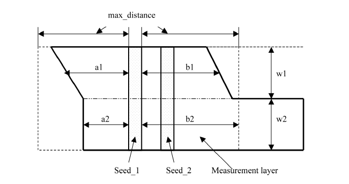
The first function (device_enclosure_vector) calculates the enclosure vector for a specified measurement layer layer_name over the device seed shape. The device seed shape must satisfy the following conditions:
- be rectangular
- be completely overlapped by measurement layer polygon
- two opposite sides of the seed shape must coincide with edges on measurement layer
In the Figure1 , the measurement layer polygon is split into trapezoids with sides that are parallel to the coincident edges of the layer and the device seed shape. Each trapezoid provides three values a, b, and w for the enclosure vector element. The max_distance parameter defines the size of the search window and so defines the maximum value for a and b.
The number of elements in the enclosure vector corresponds to the number of trapezoids and can be obtained via the SIZE field of the enclosure vector (enclosure_vector.size). As mentioned above, the enclosure vector element has three fields a, b, and w, and access to these fields can be obtained in the following way: enclosure_vector[i].a, enclosure_vector[i].b, enclosure_vector[i].w, where i is the element index.
If the measured layer covers several device seed shapes the enclosure vector is calculated for each seed shape separately. During the enclosure vector calculation all other device seed shapes are ignored. If the device seed shape doesn't satisfied the required conditions, the a, b, and w values are set to -1.
The second function (device_set_enclosure_property) is used to output the enclosure vector to a netlist in the following format:
sa1=... sb1=... sw1=... [sa2=... sb2=... sw2=... [...]]
The use of this function in a LISA generic device file is shown in Figure2.
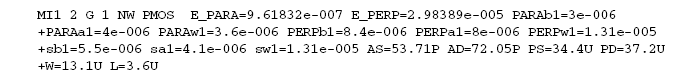
An example of netlist created by using this function in shown in Figure3 .
2.0 Function "device_enclosure"
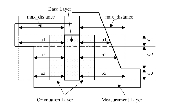
The well proximity enclosure function can be used for the calculation of well proximity and shallow trench isolation. The corresponding LISA function for Guardian LPE has the following syntax:
enclosure_vector = device_enclosure (direction, <base_layer_or_pin>, <meas_layer_or_pin>, <orient_layer_or_pin>, max_distance)
where enclosure_vector is a vector of triplets (a, b, w), direction is the measurement orientation with respect to the coincident edges of the base layer base_layer_or_pin and orientation layer orien_layer_or_pin , and can have two values ORIEN_PERPENDICULAR and ORIEN_PARALLEL , meas_layer_or_pin is the name of the measurement layer that encloses the base layer. Figure4 illustrates the function used with the orientation set to ORIEN_PERPENDICULAR and Figure5 displays the function used with the orientation set to ORIEN_PARALLEL .
The following are the function input arguments conditions:
- the base layer can be the device layer, any pin or auxiliary layer, or pin name. The base layer object must be rectangular and completely overlapped by the measurement layer polygon.
- the measurement layer can be any pin or auxiliary layer, or pin name. The measurement layer polygon must completely overlap the rectangular base layer object.
- the orientation layer can be any pin or auxiliary layer, or pin name. The polygon(s) from the orientation layer must have at least one coincident edge with the base layer object. If there are several coincident edges then all such edges should be parallel each other.
- The base, measurement and orientation layers must all be different layers.
The measurement layer polygon is split into trapezoids, with sides that are parallel to the coincident edges of the base layer rectangle and orientation layer polygon for ORIEN_PARALLEL direction argument or are perpendicular to the coincide edges for ORIEN_PERPENDICULAR direction argument.
Each trapezoid provides three values a, b, and w for the enclosure vector element (see Figure4 and Figure5 ). The max_distance parameter defines the size of the search window and so defines the maximum value for a and b.
There is an additional function device_set_named_enclosure_property which is used to output the enclosure vector with a special name to the netlist:
device_set_named_enclosure_property(<name>, enclosure_vector),
where <name> is a string variable.
The output will have the following format:
<name>a1=...<name>b1=...<name>w1=...[<name> a2=...<name>b2=...<name>w2=...[..]]
The use of these functions in a LISA generic device file is shown in Figure6.
An example of netlist created by using this function in shown in Figure7 .
3.0: Experimenting with these functions
Once all the example files have been downloaded, open an EXPERT session and open the (*.eld) file called hipex_ex09.eld . Then open the top cell "hipex_09" . A cell layout view showing a single PMOS transistor as shown in Figure8 , should open.
In this *.eld file, all the necessary derived layers are already present (layer in lower case). Therefore during the extraction, the user does not need to generate the derived layers.
Before performing the extraction of this device with all the netlist parameters, the user needs to set the proper path to the LISA generic device extraction file.
Choose Setup->Technology->Device Setup and make sure that the File Name field located at the bottom of the window points to the downloaded file "hipex_ex.lisa" .
The proper extraction setup also needs to be loaded using the menu, Verification->Extraction->Setup and choosing the Load button, the user needs to point to the downloaded file "settings_ex09.lpe" . Some paths may have to be remapped to your local installation, especially the path to the netlist being generated (located under the Netlisting tab of the window).
Once this configuration section is completed, the user can perform the extraction by choosing Verification->Extraction->Hipex-Net->Run.
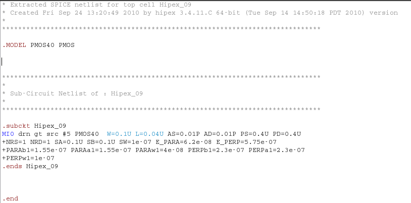
A progress window titled "Netlist Extraction in progress..." will display for a brief moment and the same window will change to a "Guardian NET" window with the message "Guardian NET run completed successfully" . In this window, press the Open Netlist button to inspect the extracted netlist. You should see the netlist shown in Figure9 .
The user can see the use of the different functions described in this example by opening the file hipex_ex.lisa . This file could be modified depending on the user needs and on what parameter names and formats is expected by the model file used for the post layout simulation.
hipex_ex09_script2.lisa
											define procedure NGATE
do begin
 W = 0.0;
 L = 0.0;
 PD = 0.0;
 PS = 0.0;
 AS = 0.0;
 AD = 0.0;

 AREA = device_area("ngate", "");
 W1 = device_perimeter(REL_BUTTING, "ngate", "S");
 W2 = device_perimeter(REL_BUTTING, "ngate", "D");
 W = (W1 + W2) / 2;
 IF (W NEQ 0.0) THEN (L = AREA / W);

 AD = device_area("D", "");
 AS = device_area("S", "");
 PD = device_perimeter(REL_NONE, "D", "");
 PS = device_perimeter(REL_NONE, "S", "");

 !!! device_enclosure_vector !!!
 ENCL_VEC = device_enclosure_vector("act", 1000.0);
 !!!

 device_set_property("L", L);
 device_set_property("W", W);
 device_set_property("PD", PD);
 device_set_property("PS", PS);
 device_set_property("AD", AD);
 device_set_property("AS", AS);

 !!! device_set_enclosure_property !!!
 device_set_enclosure_property(ENCL_VEC);
 !!!
end;
hipex_ex09_script6.lisa
											define procedure PGATE
 do begin
  W = 0.0;
  L = 0.0;
  PD = 0.0;
  PS = 0.0;
  AS = 0.0;
  AD = 0.0;

  AREA = device_area("pgate", "");
  W1 = device_perimeter(REL_BUTTING, "pgate", "S");
  W2 = device_perimeter(REL_BUTTING, "pgate", "D");
  W = (W1 + W2) / 2;

  IF (W NEQ 0.0) THEN (L = AREA / W);
  AD = device_area("D", "");
  AS = device_area("S", "");
  PD = device_perimeter(REL_NONE, "D", "");
  PS = device_perimeter(REL_NONE, "S", "");

  c = device_count("D");
  net_name = device_pin_net("S");
  device_set_property("L", L);
  device_set_property("W", W);
  device_set_property("PD", PD);
  device_set_property("PS", PS);
  device_set_property("AD", AD);
  device_set_property("AS", AS);

 ! PERP and PARA are enclosure vectors
 PERP = device_enclosure(ORIEN_PERPENDICULAR, "pgate", "nwell", "S", 1000.0);
 PARA = device_enclosure(ORIEN_PARALLEL, "pgate", "nwell", "S", 1000.0);
 N_PERP = PERP.SIZE;
 E_PERP = 0.0;
 I = 0;
 LOOP
  BEGIN
   I = I + 1;
   E_PERP = E_PERP + (PERP[I].a + PERP[I].b) * PERP[I].w;
   IF (I EQL N_PERP) THEN (LEAVE LOOP);
  END;
  E_PERP = E_PERP / L / 2;
  N_PARA = PARA.SIZE;
  E_PARA = 0.0;
  I = 0;
  LOOP
   BEGIN
    I = I + 1;
    E_PARA = E_PARA + (PARA[I].a + PARA[I].b) * PARA[I].w;
    IF (I EQL N_PARA) THEN (LEAVE LOOP);
   END;
   E_PARA = E_PARA / W / 2;

  device_set_named_enclosure_property("PERP", PERP);
  device_set_named_enclosure_property("PARA", PARA);
  device_set_property("E_PERP", E_PERP);
  device_set_property("E_PARA", E_PARA);
end;
hipex_ex09_net_cmd.lisa
											!--------------------------------------------------------------------
!Net command file
!DESIGN    : design
!TECHNO    : techno
!USER      :
!TIME      : Thu May 28 21:00:53 2020

!--------------------------------------------------------------------

! HIPEX to CUP map table

cup layer "xc_poly" /hipex_layer="poly";
cup layer "xc_metal1" /hipex_layer="metal1";

! GDS LAYER MAP

hipex layer /gds_layer=   0 /gds_type= 0 /geom_layer="actcont";
hipex layer /gds_layer=   1 /gds_type= 0 /geom_layer="poly";
hipex layer /gds_layer=   2 /gds_type= 0 /geom_layer="metal1";
hipex layer /gds_layer=  28 /gds_type= 0 /geom_layer="MET1" /text_layer="MET1_HPX_TEXT";
hipex layer /gds_layer= 256 /gds_type= 0 /geom_layer="polycont";
hipex layer /gds_layer= 257 /gds_type= 0 /geom_layer="tpdf";
hipex layer /gds_layer= 258 /gds_type= 0 /geom_layer="gate1";
hipex layer /gds_layer= 259 /gds_type= 0 /geom_layer="gt1noio";
hipex layer /gds_layer= 260 /gds_type= 0 /geom_layer="s_tpdfhv";
hipex layer /gds_layer= 261 /gds_type= 0 /geom_layer="nxwl";
hipex layer /gds_layer= 262 /gds_type= 0 /geom_layer="pgate";
hipex layer /gds_layer= 263 /gds_type= 0 /geom_layer="pthn";
hipex layer /gds_layer= 264 /gds_type= 0 /geom_layer="acti";
hipex layer /gds_layer= 265 /gds_type= 0 /geom_layer="HPX$pgate";

! TEXT TYPES


! PORT LAYERS


! SOFT LAYERS

hipex soft_layer "nxwl" /link="";

! MISC (optional) statementsS


! CONNECTIVITY

hipex connect "actcont";
hipex connect "gate1" "poly";
hipex connect "gt1noio" "poly";
hipex connect "metal1";
hipex connect "metal1" "poly" /contact="polycont";
hipex connect "metal1" "actcont";
hipex connect "metal1" "polycont";
hipex connect "metal1" "tpdf" /contact="actcont";
hipex attach "MET1_HPX_TEXT" "metal1";
hipex connect "pgate";
hipex connect "poly" "pgate";
hipex connect "polycont";
hipex connect "s_tpdfhv" "tpdf";
hipex connect "tpdf";

! DEVICES TEXTS


! DEVICE DEFINITIONS

hipex generic_device "HPX$pgate" /pins=({{"tpdf", "D"}, {"pgate", "G"}, {"tpdf", "S"}, {"nxwl", "SUB"}}) /auxs={"pthn", "acti"} /by_shape /func="pgate" /element_name="PMOS" /model_name="PMOS40";
Include("/home/alexa/2020_06/09/hipex_ex.lisa");

! GEOMETRICAL OPERATIONS

    hipex copy "pgate" "HPX$pgate";


! SOFT/WELL CHECKS

hipex soft_check "nxwl";

! MASKED DIELECTRIC LAYERS
hipex_ex09_opt.lisa
											!--------------------------------------------------------------------
!Run file
!DESIGN    : design
!TECHNO    : techno
!USER      :
!TIME      : Thu May 28 21:00:53 2020

!--------------------------------------------------------------------
TOP_CELL                                = "Hipex_09";

HIPEX_DB_DIRECTORY                      = "database";
!--------------------------------------------------------------------
!Extraction: LISA template command file
!--------------------------------------------------------------------

!--------------------------------------------------------------------
!Layout parameters
!--------------------------------------------------------------------
HIPEX_LAYOUT_FORMAT                     = "GDS";
HIPEX_LAYOUT_FILE                       = "Hipex_09$HPX.gds";
HIPEX_OVERLAP_INSTANCE_CHECK            = "NO";
HIPEX_SUPPRESS_NOTEMPTY                 = "YES";
HIPEX_NON45_FLAG                        = "NO";

!--------------------------------------------------------------------
!Connectivity parameters
!--------------------------------------------------------------------
HIPEX_TERNARY_CONNECT_THROUGH_TOUCH     = "NO";

!--------------------------------------------------------------------
!Output parameters
!--------------------------------------------------------------------
HIPEX_COMMENT_MODEL                     = "NO";
HIPEX_COMMENT_TOP_SUBCKT                = "NO";
HIPEX_HIER_SPICE_WL_NAME                = "/home/alexa/2020_06/09/Hipex_09_hier.spice";
HIPEX_MOSFET_LW_ONLY                    = "NO";
HIPEX_MOSFET_EXCLUDE_W_SD               = "NO";
HIPEX_OUTPUT_SPICE_ATTRIBUTES           = "YES";
HIPEX_CAP_OUTPUT_LW                     = "NO";
HIPEX_RES_OUTPUT_LW                     = "YES";
HIPEX_CAP_OUTPUT_AREA_PERIMETER         = "YES";
HIPEX_OUTPUT_SPICE_FORMAT               = "HSPICE";
HIPEX_PININFO                           = "NO";
HIPEX_PRINT_MESSAGES                    = "NO";
NETLIST_OUTPUT_PM                       = "NO";
NETLIST_DISTRIBUTION_MODE               = "ACCURATE";
NETLIST_LINE_LENGTH                     = 80;
NETLIST_EXCLUDE_LIBRARY_PREFIX          = "NO";
NETLIST_GLOBALS_IN_SUBCKT_PINS          = "YES";
NETLIST_TEXTED_PINS                     = "YES";
NETLIST_LIBRARIES                       = {};

!--------------------------------------------------------------------
!ERC parameters
!--------------------------------------------------------------------
HIPEX_DANGLE_FLAG                       = "NO";
HIPEX_CAP_MESSAGE                       = "NO";
HIPEX_DIODE_MESSAGE                     = "NO";
HIPEX_RENAME_OPENS                      = "YES";
HIPEX_MULTILABEL_NAME                   = "";
HIPEX_SOFTCHECK_WARNINGS_AS_ERRORS      = "NO";

!--------------------------------------------------------------------
!Node Name parameters
!--------------------------------------------------------------------
HIPEX_HIERARCHY_SEPARATOR               = "/";
HIPEX_NODE_NAME_SEPARATOR               = "_";
HIPEX_DEFAULT_INSTANCE_PREFIX           = "I";
HIPEX_DEFAULT_NODE_PREFIX               = "#";
HIPEX_DELETE_BAD_CHAR                   = "YES";
HIPEX_XY_LOCATION                       = "NO";
HIPEX_CASE_SENSITIVE_NET_NAMES          = "YES";
HIPEX_AUTOGENERATE_LOCAL                = "YES";
POWER_NODE                              = {};
GROUND_NODE                             = {};
GLOBAL_TEXT_LIST                        = {};
HIPEX_PIN_DELIMITER                     = ":";

!--------------------------------------------------------------------
!Explosion parameters
!--------------------------------------------------------------------
HIPEX_WIRING_EXPLODE                    = "NO";
HIPEX_KEEP_FLATTEN_CELLS                = "YES";
HIPEX_TEXT_TOP                          = "YES";
HIPEX_TEXT_DEPTH                        = 0;
HIPEX_AUTO_EXPLODE                      = "NO";
HIPEX SET_CELL_OPTIONS {"Hipex_09"} /EXPLODE;

!--------------------------------------------------------------------
!Pins parameters
!--------------------------------------------------------------------
HIPEX_IGNORE_DANGLE_PINS                = "YES";

!--------------------------------------------------------------------
!BackAnnotate parameters
!--------------------------------------------------------------------
HIPEX_BACKANNOTATE                      = "NO";

!--------------------------------------------------------------------
!Capacitance Extraction parameters
!--------------------------------------------------------------------
CPX_COUPLED_THRESHOLD                   = 0.0;
CPX_EXTRACT_DANGLES                     = "NO";
CPX_OUTPUT_DUMMY_CAPA                   = "NO";
CPX_FIELD_SOLVER                        = "NO";

!--------------------------------------------------------------------
!Field Solver C-extraction (Stellar) parameters
!--------------------------------------------------------------------
CPX_STEP_X                              = 0.5;
CPX_STEP_Y                              = 0.5;
CPX_STEP_Z                              = 0.5;
CPX_PRECISION                           = 0.01;
CPX_MAX_ITER                            = 100;
CPX_DECOMPOSITION                       = "YES";
CPX_DEC_STEP                            = "NO";
CPX_DEC_VALUE                           = -1.0;
CPX_BOX                                 = "NO";
CPX_BOX_VALUES_XMIN                     = 0.0;
CPX_BOX_VALUES_XMAX                     = 0.0;
CPX_BOX_VALUES_YMIN                     = 0.0;
CPX_BOX_VALUES_YMAX                     = 0.0;
CPX_FILTER                              = "NO";
CPX_CAPA_MIN                            = 1e-20;
CPX_RENEW                               = "NO";
CPX_SAVE_FILE                           = "/home/alexa/2020_06/09/RenewSavedFile.sav";
CPX_THREED_GENERATION                   = "NO";
CPX_THREED_FILENAME                     = "/home/alexa/2020_06/09/3DStructureFile.str";

!--------------------------------------------------------------------
!Field Solver C-extraction (Clever) parameters
!--------------------------------------------------------------------

!--------------------------------------------------------------------
!Resistance Extraction parameters
!--------------------------------------------------------------------
RPX_SERIAL_MERGE_THRESHOLD              = 0.0;
RPX_OUTPUT_XY                           = "NO";
RPX_OUTPUT_LAYER_NAMES                  = "NO";
RPX_SKIP_POWER                          = "YES";
RPX_USE_TEXTS_AS_SUBNODES               = "NO";
RPX_USE_FIELD_SOLVER                    = "NO";

!--------------------------------------------------------------------
!Netlist RC Reduction parameters
!--------------------------------------------------------------------
NETLIST_CRC                             = "NO";

!--------------------------------------------------------------------
!Coefficient Units parameters
!--------------------------------------------------------------------
HIPEX SET_UNIT /CAPACITANCE "aF";
HIPEX SET_UNIT /RESISTANCE "Ohm";
HIPEX SET_UNIT /LENGTH "um";
run_net.lisa
											INCLUDE ("hipex_ex09_opt.lisa");
INCLUDE ("hipex_ex09_net_cmd.lisa");

HIPEX_SUMMARY_PATH                      = "/home/alexa/2020_06/09";
HIPEX_NET_MAIN();
hipex_ex.lisa
											!!!!!!!!!!!!!!!!!!!!!!!! PROCEDURE FOR CALCUL SA, SB and SW !!!!!!!!!!!!!!!!!!!!!!!!!!!!!!!!!!!!!!
define procedure sum_encl
parameter ENCL
parameter AB
do begin
  N_ENCL = ENCL.SIZE;
  SUM = 0;
  IF(N_ENCL NEQ 0) THEN BEGIN
	I = 0;
  	LOOP BEGIN
     I = I + 1;

    IF(AB EQL "A") THEN
      ( SUM = SUM + ENCL[I].A )
    ELSEIF (AB EQL "B") THEN
	  ( SUM = SUM + ENCL[I].B)
    ELSE
        ( SUM = SUM + ENCL[I].W);
     IF (I EQL N_ENCL) THEN (LEAVE LOOP);
   END;
END;
 IF(SUM NEQ 0) THEN
   (SUM = SUM)
 ELSE
   (SUM = 0);
end;
!! end procedure to calculate SA SB
!!!!!!!!!!!!!!!!!!!!!!!!!!!!!!!!!!!!!!!!!!!!!!!!!!!!!!!!!!!!!!!!!!!!!!!!!!!!!!!!!!!!!!!!!!!!!!!

!!!!!!!!!!!!!!!!!!!!!!!!!!!!Start of generic MOS procedure!!!!!!!!!!!!!!!!!!!!!!!!
define procedure mos
parameter rec
parameter aux1
parameter aux2
parameter aux3
parameter aux4
parameter NP
do begin
	W=(device_perimeter(REL_BUTTING,rec,aux1) + device_perimeter(REL_INSIDE,rec,aux1))/2;
	L=device_area(rec,"")/W;

   	PI_S_OD = device_perimeter(REL_INSIDE, "S",aux2);
      PI_D_OD = device_perimeter(REL_INSIDE, "D",aux2);
	IF(PI_S_OD EQL 0) THEN BEGIN
		AD = device_area("D","") * W / PI_D_OD;
		AS = AD;
		PD = device_perimeter(REL_NONE,"D","") * W /PI_D_OD;
		PS = PD; END
	ELSEIF (PI_D_OD EQL 0) THEN BEGIN
		AS = device_area("S","") * W / PI_S_OD;
		AD = AS;
		PS = Device_perimeter(REL_NONE, "S","") * W /PI_S_OD;
		PD = PS; END
	ELSE BEGIN
		AS = device_area("S","") * W / PI_S_OD;
		AD = device_area("D","") * W / PI_D_OD;
		PS = device_perimeter(REL_NONE, "S","") * W /PI_S_OD;
		PD = device_perimeter(REL_NONE,"D","") * W /PI_D_OD;
	END;
!______________________________________________________
! calculation SA and SB
  ENCL = device_enclosure_vector(aux2, 60);
  SA = sum_encl(ENCL, "A");
  SB = sum_encl(ENCL, "B");
  SW = sum_encl(ENCL, "W");
!_______________________________________________________
!WELL PROXIMITY... SCH and SCV are enclosure vectors
   SCH=device_enclosure(ORIEN_PERPENDICULAR, rec, aux4, "S", 5);
   SCV=device_enclosure(ORIEN_PARALLEL, rec, aux4, "S", 5);

  N_PERP = SCH.SIZE;
  E_PERP = 0.0;
  I = 0;
  LOOP
   BEGIN
    I = I + 1;
     E_PERP = E_PERP + (SCH[I].a + SCH[I].b) * SCH[I].w;
 !   E_PERP = E_PERP + (PROX_PERP[I].a + PROX_PERP[I].b) * PROX_PERP[I].w;
    IF (I EQL N_PERP) THEN (LEAVE LOOP);
   END;
  E_PERP = E_PERP / L / 2;

 ! N_PARA = PROX_PARA.SIZE;
  N_PARA = SCV.SIZE;
  E_PARA = 0.0;
  I = 0;
  LOOP
   BEGIN
    I = I + 1;
!    E_PARA = E_PARA + (PROX_PARA[I].a + PROX_PARA[I].b) * PROX_PARA[I].w;
    E_PARA = E_PARA + (SCV[I].a + SCV[I].b) * SCV[I].w;
    IF (I EQL N_PARA) THEN (LEAVE LOOP);
   END;
  E_PARA = E_PARA / W / 2;

!_______________________________________________________
NRS = AS / W / W;
NRD = AD / W / W;

!_______________________________________________________
! Netlist parameters print out section.

	device_set_named_enclosure_property("PERP", SCH);
      device_set_named_enclosure_property("PARA", SCV);
      device_set_property("E_PERP", E_PERP);
      device_set_property("E_PARA", E_PARA);
	device_set_property("SW", SW);
	device_set_property("SB", SB);
	device_set_property("SA", SA);
	device_set_property("NRD", NRD);
	device_set_property("NRS", NRS);
	device_set_property("PD", PD);
	device_set_property("PS", PS);
	device_set_property("AD", AD);
	device_set_property("AS", AS);
	device_set_property("L", L);
	device_set_property("W", W);

end;

!!!!!!!!!!!!!!!!!!!!!!!!!!!! End of generic MOS procedure !!!!!!!!!!!!!!!!!!!!!!!!

!!!!!!!!!!!!!!!!!!!!!!!!!!!! Device definition section !!!!!!!!!!!!!!!!!!!!!!!!

!!!!!!!!!!!!!!!!!!!!!!!!!! M(PMOS)
define procedure pgate
do begin
	rec="pgate";aux1="tpdf";aux2="pthn";aux3="acti";aux4="nxwl";
	mos(rec,aux1,aux2,aux3,aux4,"P");
end;