15 : Domain Decomposition in Hipex Parasitic Capacitance Extraction
Minimum Required Versions: Expert 5.2204.3.R, Hipex 3.8.7.R
This example demonstrates running Hipex Parasitic Capacitance Extraction in Domain Decomposition mode using Field Solvers. The functionality is available for Linux only.
The layout decomposition is used in the both solver engines and in the 3D structure builder to process layouts of large size. Two ways of decomposition are supported by Hipex for parasitic capacitance extraction:
- Stripe decomposition
- Box decomposition
Hipex forms a set of overlapped partial layouts (original stripes/boxes extended with vicinities, and vicinity areas themselves) to build a series of virtual 3D structures (see Figure1 ). These structures are simulated separately, and then results are combined (using proprietary non-duplicating technique) to produce parasitic capacitors for the whole layout.
Parallel computations are used for the both 3D structure building (by running simultaneously multiple instances of Victory Process) and for Field Solver calculations (by running simultaneously multiple instances of Victory RCx or using multithreading in Stellar solver).
Domain decomposition shows promising results for Field Solver capacitance extraction. Without noticeable sacrifice of accuracy, it dramatically increases the performance of extraction. Decomposition is a way to obtain accurate extraction for layouts too big in size to be processed in one piece.
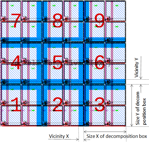
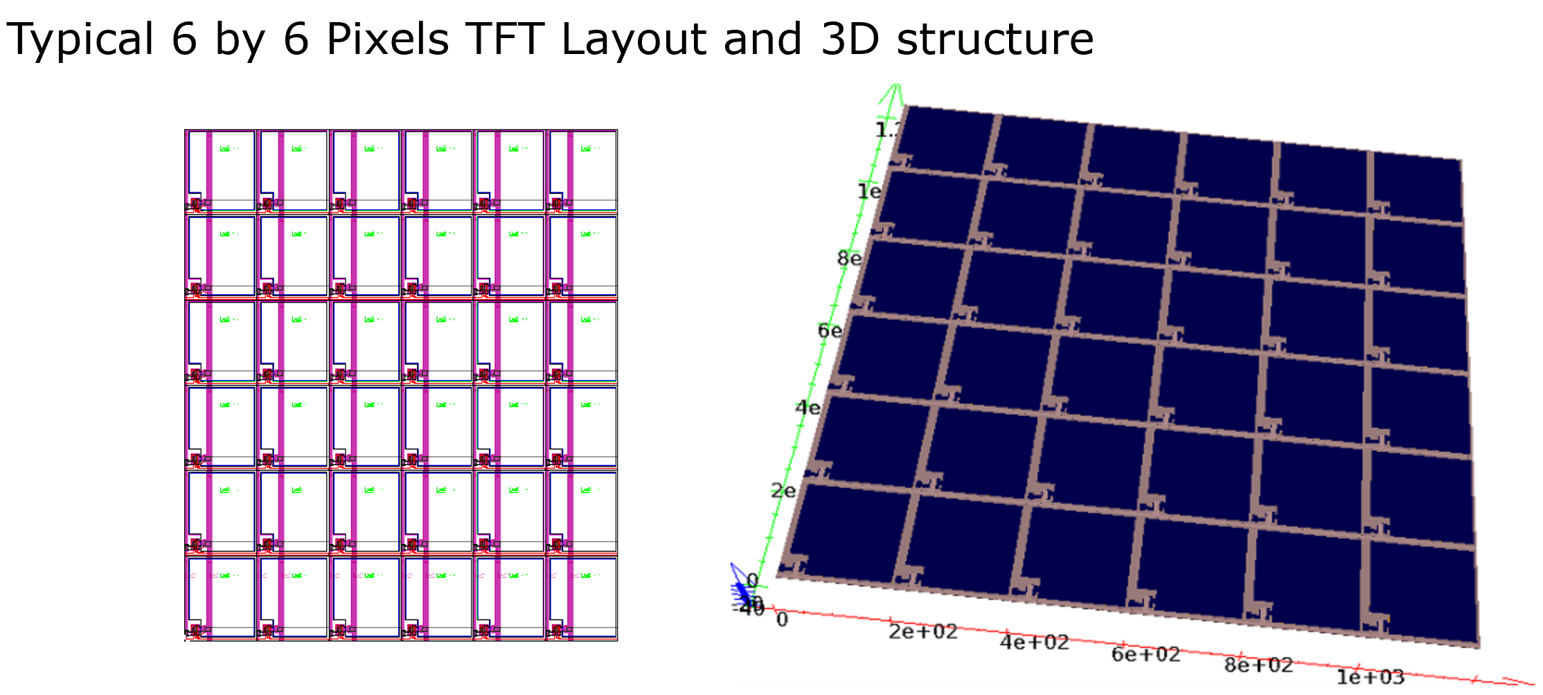
We will demonstrate domain decomposition on 6 by 6 pixels non-planar TFT layout (see Figure2 ).
1: Start Expert
Run Expert layout editor (either with the command "expert &" or by clicking the "Expert" icon).
2: Load GDS file
Choose File->Import... menu command. In appeared Import Project dialog:
- select GDS II in the File type control;
- choose the array_of_pixel2_6x6.gds file using dialog's file browser;
- choose technology file techfiles/hipex/tft.tcn using the Technology control;
- click the Open button;
- choose the array_of_pixel2_6x6 cell to open for extraction.
3: Load Extraction Settings
Select Verification->Extraction->Setup command to open the "Layout Parameter Extraction Setup" dialog. Press the Load button, and choose the array_of_pixel2_6x6_240_300_50_50.lpe file to load required extraction settings.
4: Set device directory
Before performing the extraction of the devices with all the netlist parameters, the user needs to set the proper path to the LISA generic device extraction file. Select Setup->Technology->Device Path Setup command to open the "Device Path Setup" dialog. Specify the <...>/techfiles/hipex directory name in the LISA files directory control and press the Set button.
5: Verify parasitic capacitance extraction settings in Domain Decomposition mode
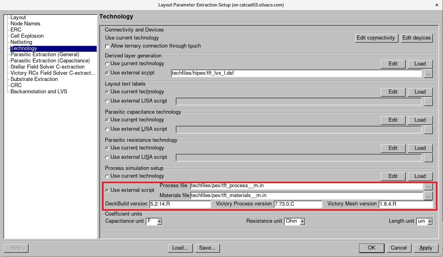
- Make sure the techfiles/pex/tft_process__m.in process and the techfiles/pex/tft_materials__m.in materials files are specified in the Process file and Materials file edit lines in the "Technology" tab of the "LPE Setup" dialog (see Figure3 ).
- Make sure the appropriate versions of DeckBuild, Victory Process and Victory Mesh are specified (if needed) in the Process simulation setup section in the "Technology" tab of the "LPE Setup" dialog (see Figure3 ).
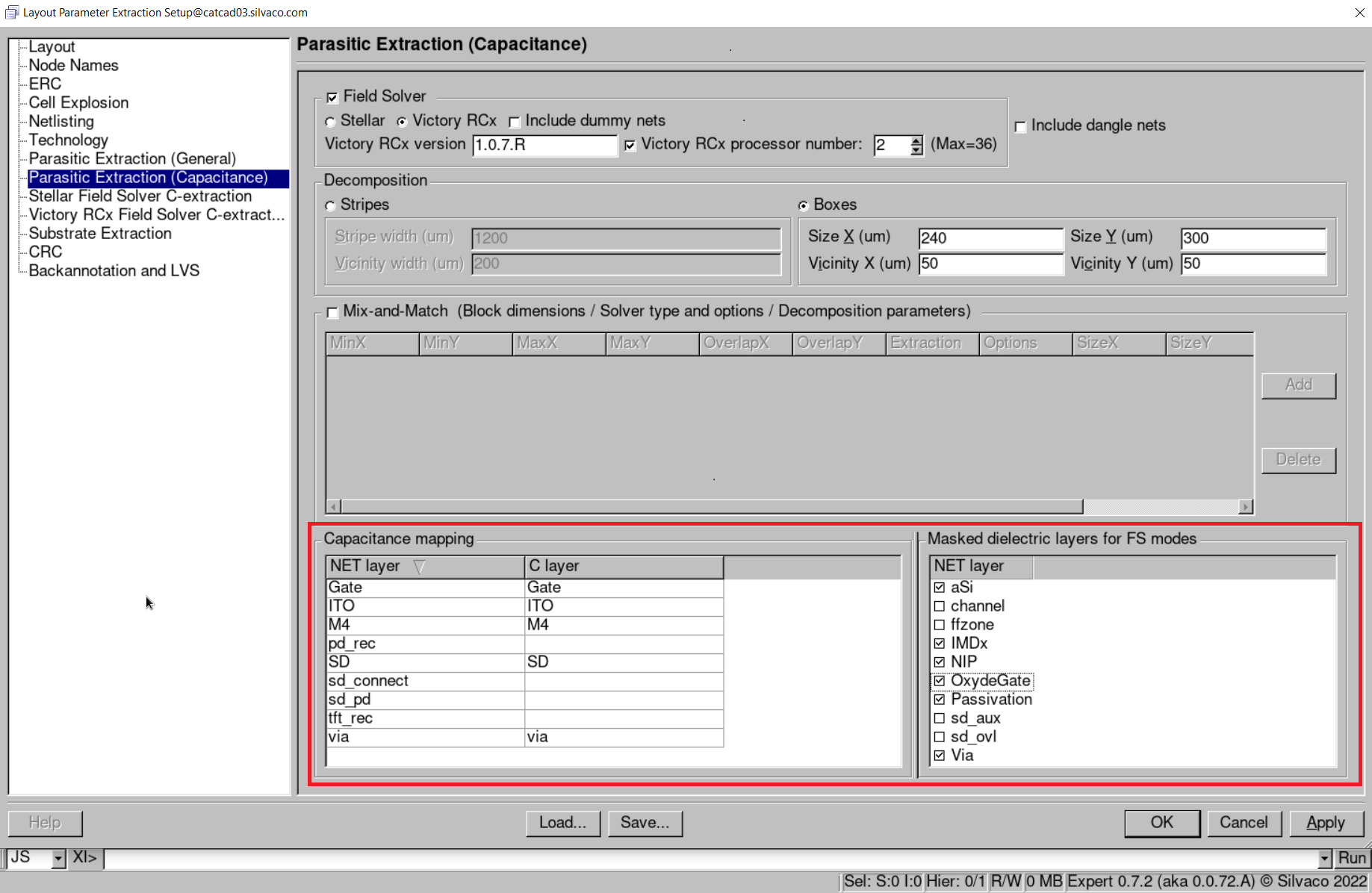
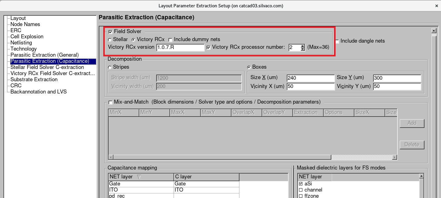
- Verify capacitance mapping and mapping of masked dielectric layers in the "Parasitic Extraction (Capacitance)" tab of the "LPE Setup" dialog to ensure proper mask usage in process description (see Figure4 ).
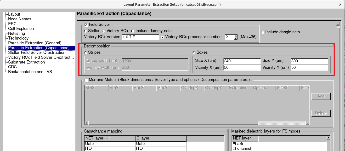
- Make sure the Boxes radio button is turned on and the appropriate values of Size and Vicinity settings are specified in the Decomposition group box in the "Parasitic Extraction (Capacitance)" tab of the "LPE Setup" dialog (see Figure5 ).
- Make sure the Victory RCx radio button is turned on and the appropriate version of Victory RCx is specified (if needed) in the Field Solver button group in the "Parasitic Extraction (Capacitance)" tab of the "LPE Setup" dialog (see Figure6 ).
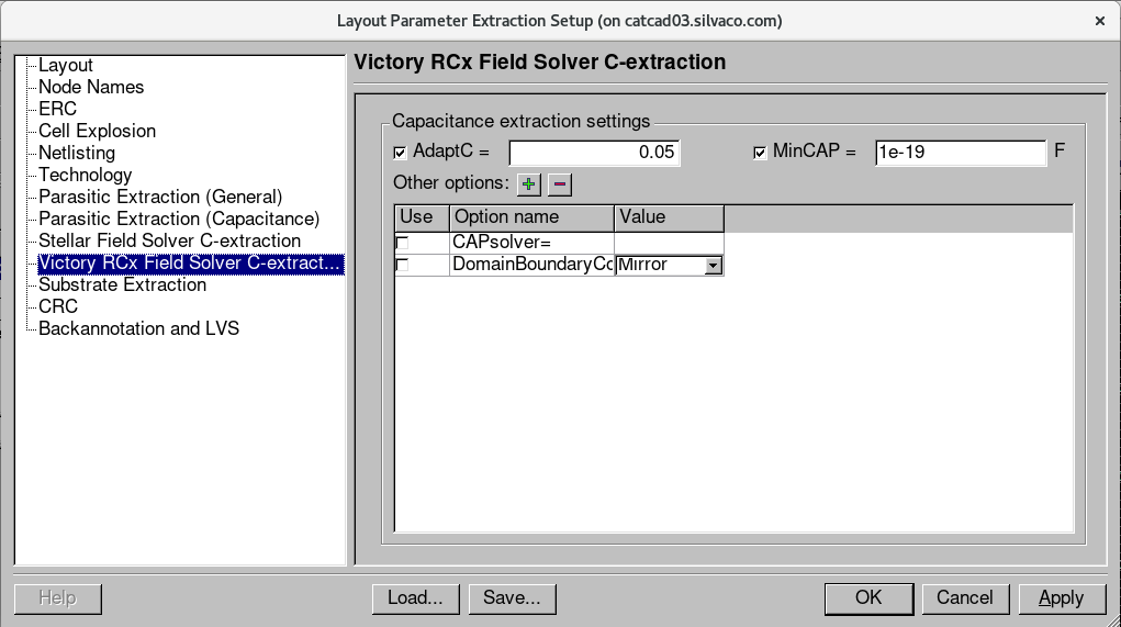
- Specify the extraction parameters in the "Victory RCx Field Solver C-extraction" tab of the "LPE Setup" dialog (see Figure7 ).
6: Performing extraction.
First, run netlist extraction with Verification->Extraction->Net->Run command from the main Expert window. Then, run parasitic capacitance extraction with Verification->Extraction->C->Run command. Press the Open Netlist button to view capacitance netlist.
tft.tcn
[an error occurred while processing this directive]
run_c.lisa
											INCLUDE ("array_of_pixel2_6x6_opt.lisa");
INCLUDE ("array_of_pixel2_6x6_net_cmd.lisa");

HIPEX_SUMMARY_PATH                      = "/home/alexa/webexaples/15";
HDB READ;
print("Writing Box Database  ...");
HDB WRITE_BOXES /FULL  "default" 240 300 50 50;
print("Boxes OK.");
CPX MAIN "default" /rewrite /box;
netlist spice/hier/c "/home/alexa/webexaples/15/array_of_pixel2_6x6_c_hier.spice";
array_of_pixel2_6x6_opt.lisa
											!--------------------------------------------------------------------
!Run file
!DESIGN    : design
!TECHNO    : techno
!USER      :
!TIME      : Thu Jun  9 22:52:35 2022

!--------------------------------------------------------------------
TOP_CELL                                = "array_of_pixel2_6x6";

HIPEX_DB_DIRECTORY                      = "database";
!--------------------------------------------------------------------
!Extraction: LISA template command file
!--------------------------------------------------------------------

!--------------------------------------------------------------------
!Layout parameters
!--------------------------------------------------------------------
HIPEX_LAYOUT_FORMAT                     = "GDS";
HIPEX_LAYOUT_FILE                       = "array_of_pixel2_6x6$HPX.gds";
HIPEX_OVERLAP_INSTANCE_CHECK            = "NO";
HIPEX_SUPPRESS_NOTEMPTY                 = "YES";
HIPEX_NON45_FLAG                        = "NO";

!--------------------------------------------------------------------
!Connectivity parameters
!--------------------------------------------------------------------
HIPEX_TERNARY_CONNECT_THROUGH_TOUCH     = "NO";

!--------------------------------------------------------------------
!Output parameters
!--------------------------------------------------------------------
HIPEX_COMMENT_MODEL                     = "YES";
HIPEX_COMMENT_TOP_SUBCKT                = "NO";
HIPEX_HIER_SPICE_WL_NAME                = "/home/alexa/webexaples/15/array_of_pixel2_6x6_hier.spice";
HIPEX_MOSFET_LW_ONLY                    = "NO";
HIPEX_MOSFET_EXCLUDE_W_SD               = "NO";
HIPEX_OUTPUT_SPICE_ATTRIBUTES           = "YES";
HIPEX_CAP_OUTPUT_LW                     = "NO";
HIPEX_RES_OUTPUT_LW                     = "YES";
HIPEX_CAP_OUTPUT_AREA_PERIMETER         = "YES";
HIPEX_OUTPUT_SPICE_FORMAT               = "HSPICE";
HIPEX_PININFO                           = "NO";
HIPEX_PRINT_MESSAGES                    = "NO";
NETLIST_OUTPUT_PM                       = "NO";
NETLIST_DISTRIBUTION_MODE               = "ACCURATELADDER";
NETLIST_LINE_LENGTH                     = 80;
NETLIST_EXCLUDE_LIBRARY_PREFIX          = "NO";
NETLIST_GLOBALS_IN_SUBCKT_PINS          = "YES";
NETLIST_TEXTED_PINS                     = "NO";
NETLIST_LIBRARIES                       = {};

!--------------------------------------------------------------------
!ERC parameters
!--------------------------------------------------------------------
HIPEX_DANGLE_FLAG                       = "YES";
HIPEX_CAP_MESSAGE                       = "NO";
HIPEX_DIODE_MESSAGE                     = "NO";
HIPEX_RENAME_OPENS                      = "YES";
HIPEX_MULTILABEL_NAME                   = "";
HIPEX_SOFTCHECK_WARNINGS_AS_ERRORS      = "NO";

!--------------------------------------------------------------------
!Node Name parameters
!--------------------------------------------------------------------
HIPEX_HIERARCHY_SEPARATOR               = "/";
HIPEX_NODE_NAME_SEPARATOR               = "_";
HIPEX_DEFAULT_INSTANCE_PREFIX           = "I";
HIPEX_DEFAULT_NODE_PREFIX               = "#";
HIPEX_DELETE_BAD_CHAR                   = "YES";
HIPEX_XY_LOCATION                       = "NO";
HIPEX_CASE_SENSITIVE_NET_NAMES          = "YES";
HIPEX_AUTOGENERATE_LOCAL                = "YES";
POWER_NODE                              = {};
GROUND_NODE                             = {"Subs"};
GLOBAL_TEXT_LIST                        = {"Subs"};
HIPEX_PIN_DELIMITER                     = ":";

!--------------------------------------------------------------------
!Explosion parameters
!--------------------------------------------------------------------
HIPEX_WIRING_EXPLODE                    = "NO";
HIPEX_KEEP_FLATTEN_CELLS                = "YES";
HIPEX_TEXT_TOP                          = "NO";
HIPEX_AUTO_EXPLODE                      = "NO";
HIPEX SET_CELL_OPTIONS {"pixel2"} /EXPLODE;
HIPEX SET_CELL_OPTIONS {"array_of_pixel2_6x6"} /EXPLODE;

!--------------------------------------------------------------------
!Pins parameters
!--------------------------------------------------------------------
HIPEX_IGNORE_DANGLE_PINS                = "YES";

!--------------------------------------------------------------------
!BackAnnotate parameters
!--------------------------------------------------------------------
HIPEX_BACKANNOTATE                      = "NO";

!--------------------------------------------------------------------
!Process Simulation and Materials parameters
!--------------------------------------------------------------------
HIPEX_PROCESS_FILE                      = "../techfiles/pex/tft_process__m.in";
HIPEX_MATERIALS_FILE                    = "../techfiles/pex/tft_materials__m.in";
HIPEX_DECKBUILD_VERSION                 = "5.2.14.R";
HIPEX_VICTORY_PROCESS_VERSION           = "7.76.1.R";
HIPEX_VICTORY_MESH_VERSION              = "1.8.4.R";

!--------------------------------------------------------------------
!Capacitance Extraction parameters
!--------------------------------------------------------------------
CPX_COUPLED_THRESHOLD                   = 0.0;
CPX_EXTRACT_DANGLES                     = "NO";
CPX_OUTPUT_DUMMY_CAPA                   = "NO";
CPX_FIELD_SOLVER                        = "VICTORYRCX";

!--------------------------------------------------------------------
!Stellar Field Solver C-extraction parameters
!--------------------------------------------------------------------
CPX_STEP_X                              = 0.5;
CPX_STEP_Y                              = 0.5;
CPX_STEP_Z                              = 0.5;
CPX_PRECISION                           = 0.01;
CPX_MAX_ITER                            = 100;
CPX_BOX                                 = "NO";
CPX_BOX_VALUES_XMIN                     = 0.0;
CPX_BOX_VALUES_XMAX                     = 0.0;
CPX_BOX_VALUES_YMIN                     = 0.0;
CPX_BOX_VALUES_YMAX                     = 0.0;
CPX_FILTER                              = "NO";
CPX_CAPA_MIN                            = 1e-20;
CPX_RENEW                               = "NO";
CPX_SAVE_FILE                           = "/home/alexa/webexaples/15/RenewSavedFile.sav";

!--------------------------------------------------------------------
!Victory RCx Capacitance Extraction parameters
!--------------------------------------------------------------------
CPX_VICTORYRCX_EXTRACTION_FILE          = "array_of_pixel2_6x6_victoryrcx_c_cmd.in";
CPX_VICTORYRCX_VERSION                  = "1.0.7.R";
CPX_VICTORYRCX_PARALLEL_MODE            = "YES";
CPX_VICTORYRCX_CPU_NUMBER               = 2;

!--------------------------------------------------------------------
!Resistance Extraction parameters
!--------------------------------------------------------------------
RPX_SERIAL_MERGE_THRESHOLD              = 0.0;
RPX_OUTPUT_XY                           = "YES";
RPX_OUTPUT_LAYER_NAMES                  = "YES";
RPX_SKIP_POWER                          = "YES";
RPX_USE_TEXTS_AS_SUBNODES               = "NO";
RPX_USE_FIELD_SOLVER                    = "NO";

!--------------------------------------------------------------------
!Netlist RC Reduction parameters
!--------------------------------------------------------------------
NETLIST_CRC                             = "NO";

!--------------------------------------------------------------------
!Substrate Extraction parameters
!--------------------------------------------------------------------
SPX_RUN_SIPEX                           = "NO";
SPX_MODE                                = "SIPEX";
SPX_SILICON_THICKNESS                   = 300.0;
SPX_BACKSIDE                            = "CONDUCTIVE_CONNECTED";
SPX_BACKSIDE_NODE                       = "cwsBackside";
SPX_INCLUDE_BACKSIDE_MODEL              = "NO";
SPX_BACKSIDE_THICKNESS                  = 10.0;
SPX_BACKSIDE_CONDUCTIVITY               = 3.3e-10;
SPX_BACKSIDE_PERMITTIVITY               = 6.2;
SPX_SIPEX_MANUFACTURING_DATABASE        = "";

!--------------------------------------------------------------------
!Coefficient Units parameters
!--------------------------------------------------------------------
HIPEX SET_UNIT /CAPACITANCE "F";
HIPEX SET_UNIT /RESISTANCE "Ohm";
HIPEX SET_UNIT /LENGTH "um";
array_of_pixel2_6x6_net_cmd.lisa
											!--------------------------------------------------------------------
!Net command file
!DESIGN    : design
!TECHNO    : techno
!USER      :
!TIME      : Thu Jun  9 22:51:07 2022

!--------------------------------------------------------------------

! HIPEX to CUP map table

cup layer "Gate" /hipex_layer="Gate";
cup layer "M4" /hipex_layer="M4";
cup layer "SD" /hipex_layer="SD";
cup layer "ITO" /hipex_layer="ITO";
cup layer "via" /hipex_layer="via";

! GDS LAYER MAP

hipex layer /gds_layer=   0 /gds_type= 0 /geom_layer="tft_rec";
hipex layer /gds_layer=   1 /gds_type= 0 /geom_layer="Gate" /text_layer="_HPX_TEXT_Gate";
hipex layer /gds_layer=   4 /gds_type= 0 /geom_layer="Via";
hipex layer /gds_layer=   5 /gds_type= 0 /geom_layer="M4" /text_layer="_HPX_TEXT_M4";
hipex layer /gds_layer=   8 /gds_type= 0 /geom_layer="NIP";
hipex layer /gds_layer=  11 /gds_type= 0 /geom_layer="SD" /text_layer="_HPX_TEXT_SD";
hipex layer /gds_layer=  70 /gds_type= 0 /geom_layer="IMDx";
hipex layer /gds_layer=  71 /gds_type= 0 /geom_layer="OxydeGate";
hipex layer /gds_layer=  72 /gds_type= 0 /geom_layer="ITO";
hipex layer /gds_layer=  74 /gds_type= 0 /geom_layer="aSi";
hipex layer /gds_layer=  80 /gds_type= 0 /geom_layer="Passivation";
hipex layer /gds_layer=  81 /gds_type= 0 /geom_layer="via";
hipex layer /gds_layer=  82 /gds_type= 0 /geom_layer="pd_rec";
hipex layer /gds_layer=  83 /gds_type= 0 /geom_layer="sd_pd";
hipex layer /gds_layer=  84 /gds_type= 0 /geom_layer="sd_connect";
hipex layer /gds_layer=  85 /gds_type= 0 /geom_layer="channel";
hipex layer /gds_layer=  86 /gds_type= 0 /geom_layer="sd_ovl";
hipex layer /gds_layer=  87 /gds_type= 0 /geom_layer="sd_aux";
hipex layer /gds_layer=  88 /gds_type= 0 /geom_layer="ffzone";

! TEXT TYPES


! PORT LAYERS


! SOFT LAYERS


! MISC (optional) statementsS


! CONNECTIVITY

hipex attach "_HPX_TEXT_Gate" "Gate";
hipex connect "ITO" "M4" /contact="via";
hipex connect "M4" "Gate" /contact="via";
hipex attach "_HPX_TEXT_M4" "M4";
hipex attach "_HPX_TEXT_SD" "SD";
hipex connect "sd_connect" "SD";
hipex connect "sd_connect" "M4" /contact="via";
hipex attach "_HPX_TEXT_SD" "sd_connect";
hipex connect "sd_pd" "sd_connect";

! DEVICES TEXTS


! DEVICE DEFINITIONS

hipex generic_device "tft_rec" /pins=({{"sd_connect", "D"}, {"Gate", "G"}, {"sd_connect", "S"}}) /auxs={"sd_ovl", "channel", "sd_aux"} /by_shape /func="tft" /element_name="NMOS" /model_name="TFT";
hipex generic_device "pd_rec" /pins=({{"ITO", "POS"}, {"sd_pd", "NEG"}}) /auxs={"ffzone"} /by_shape /func="pd" /element_name="D" /model_name="PD";
Include("/home/viktarm/examples/hipex/2022_04_01/15/techfiles/hipex/tft_lvs_d.lisa");

! SOFT/WELL CHECKS


! MASKED DIELECTRIC LAYERS

cup masked dielectric layer "IMDx";
cup masked dielectric layer "NIP";
cup masked dielectric layer "OxydeGate";
cup masked dielectric layer "Passivation";
cup masked dielectric layer "Via";
cup masked dielectric layer "aSi";

! SUBSTRATE EXTRACTION LAYERS
array_of_pixel2_6x6_victoryrcx_c_cmd.in
											#go victoryrcx

interconnect capacitance AdaptC=0.05 minCAP=1e-19
tft_process__m.in
											go victoryp
init depth=10 oxide GasHeight=10 separate.layers

# Metal gate
deposit material=aluminum_m thickness=0.12 max
mask "Gate"
etch material=aluminum_m thickness=0.12 max
strip resist
electrodes "Gate"  material=aluminum_m

# Gate Oxide
deposit material=SiN_m thickness=0.15 conformal

# Active Amorphous Silicon
deposit material=aSi_m thickness=0.033 conformal
mask "aSi"
etch material=aSi_m max
strip resist


# Nitride Hard Mask
deposit material=SiN_m thickness=0.135 conformal

# Source-Drain Contacts
deposit material=Cr_m thickness=0.12 conformal
mask "SD"
etch material=Cr_m max
strip resist
electrodes "SD"  material=Cr_m

# NIP
deposit material=t_silicon_m thickness=1.8 conformal
mask "NIP"
etch material=t_silicon_m max
strip resist

# ITO
deposit material=ITO_m thickness=0.06 conformal
mask "ITO"
etch material=ITO_m max
strip resist
electrodes "ITO"  material=ITO_m

# IMDx
deposit material=SiON_m thickness=2.072 conformal
mask "IMDx"
etch material=SiON_m max
strip resist


# Top Metal
deposit material=M4aluminum_m thickness=0.646 conformal
mask "M4"
etch material=M4aluminum_m max
strip resist
electrodes "M4" material=M4aluminum_m

# Passivation
deposit material=Passiv_m thickness=2.25 max


# Via
##mask "Via" reverse
##etch material("Passiv") max
##strip resist

save name=""
tft_materials__m.in
											material  material("aluminum_m")   conductivity=376676
material  material("aSi_m")   permittivity=7.514
material  material("Cr_m")   conductivity=5000
material  material("ITO_m")   conductivity=5000
material  material("Passiv_m")  permittivity=9.225
material  material("SiN_m")  permittivity=6.21
material  material("t_silicon_m")  permittivity=16.5
material  material("SiON_m")  permittivity=7.82
material  material("M4aluminum_m") conductivity=5000