10 : Extraction of Analog (RF) Design
Minimum Required Versions: Expert5.2204.3.R, Hipex 3.8.7.R
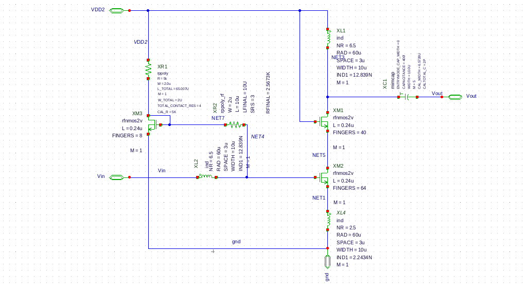
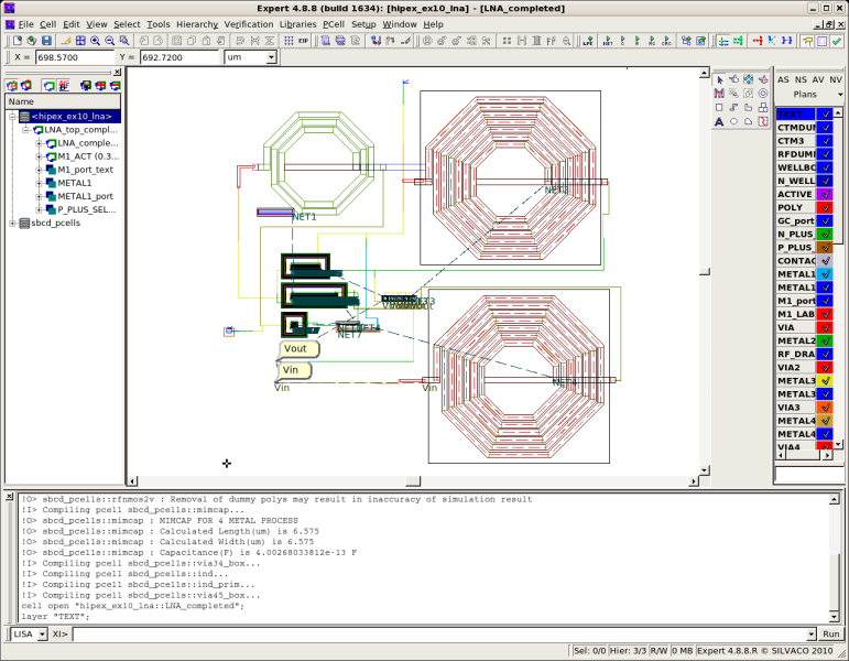
The example circuit for Analog(RF) netlist extraction is the Low Noise Amlpifier (LNA) shown at figure1 . This single ended cascode design uses three 2Volt RF nmos transistors and three spiral inductors. Instructions for simulating the LNA and the use of the Gateway schematic editor and SmartSpiceRF simulation are given in the Radio Frequency Demo PDK. We will concentrate on the setup of the RF Layout design in EXPERT and the extraction of netlists with Hipex in this example. The layout design was done using the Netlist Driven Layout (NDL) flow from Gateway to Expert where an NDL netlist with device placement coordinates is generated in Gateway and imported into Expert as the initial placement of the devices showing flight lines where the devices need to be wired to each other.
1.0 Loading The Example Circuit into Expert
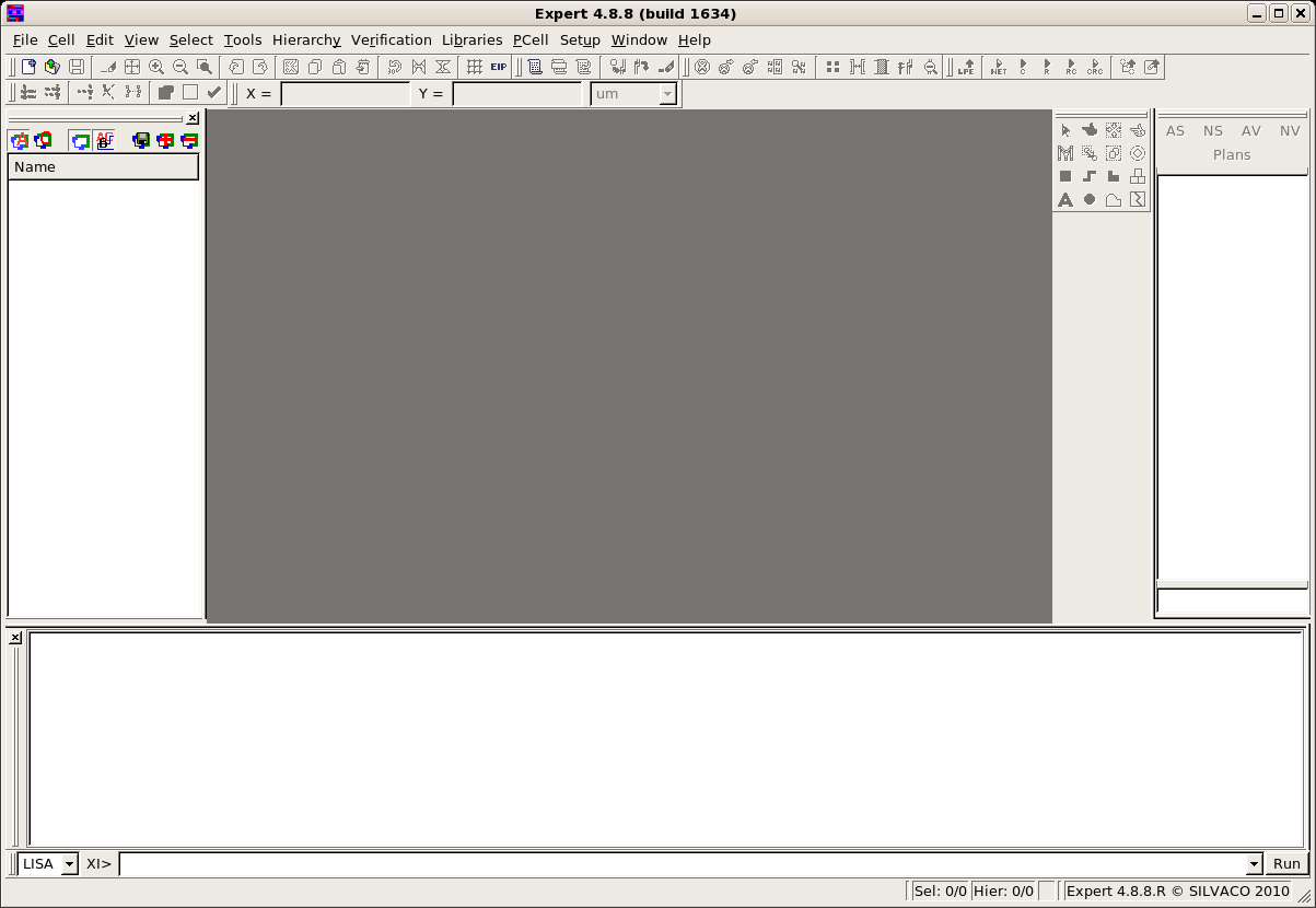
- Start Expert Layout Editor (with "expert &" on Linux or from the "Expert" desktop shortcut on Windows). Expert will start with a blank new session ( figure2 ).
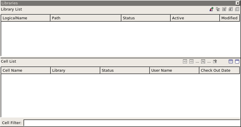
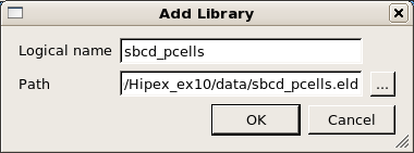
- Configure EXPERT to access the Pcell library by selecting Library->Setup. The Library Setup window will appear ( figure3 ).Click Add, locate the file simucad_demo_pcells.eld (in this case it is under./pcells/), and click OK ( figure4 ). Press "Activate" icon (second from right in the upper line of controls) in Library Setup window to make pcells loadable. Close Library Setup window.
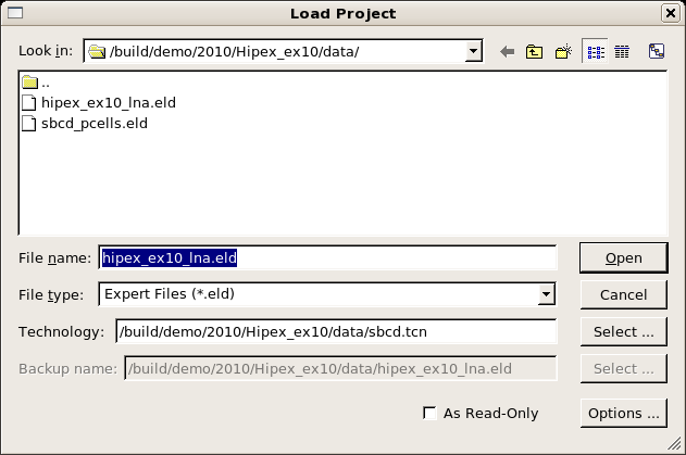
- Load the LNA layout. For this, select File->Open and the Load Project dialog box will appear( figure5 ). Select the demo_sbcd.tcn as the technology file. If the Technology field is not accessible, click on the Options button in the lower right and select "use external technology for eld files" and also make sure that the option is set "Identify layers by name". The technology file has definitions which will be used for Netlist Extraction later.
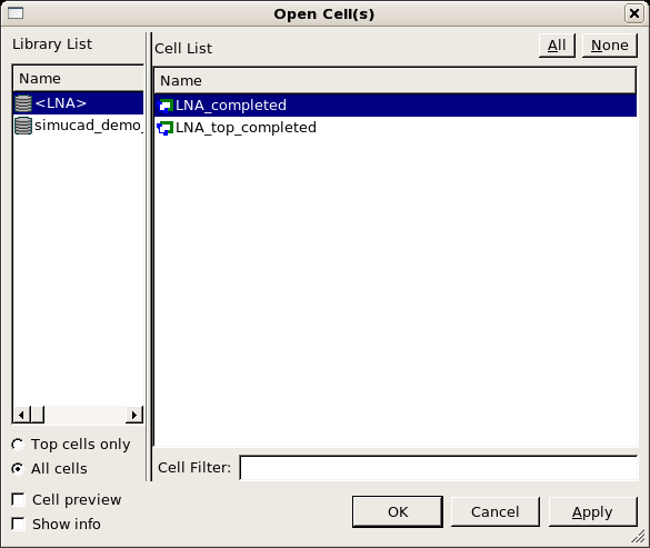
Open the file LNA.eld . Press the Open button to open the selected file and the Cell Open dialog box will appear ( figure6 ). Open the LNA_completed cell to load the LNA layout ( figure7 ).
2.0 Configuring Layout Extraction
EXPERT offers built-in interface to provide communication to the Netlist Extraction (NLE) and Layout Parasitic Extraction (LPE) tools of Hipex family.
2.1. Configuring Netlist Extraction
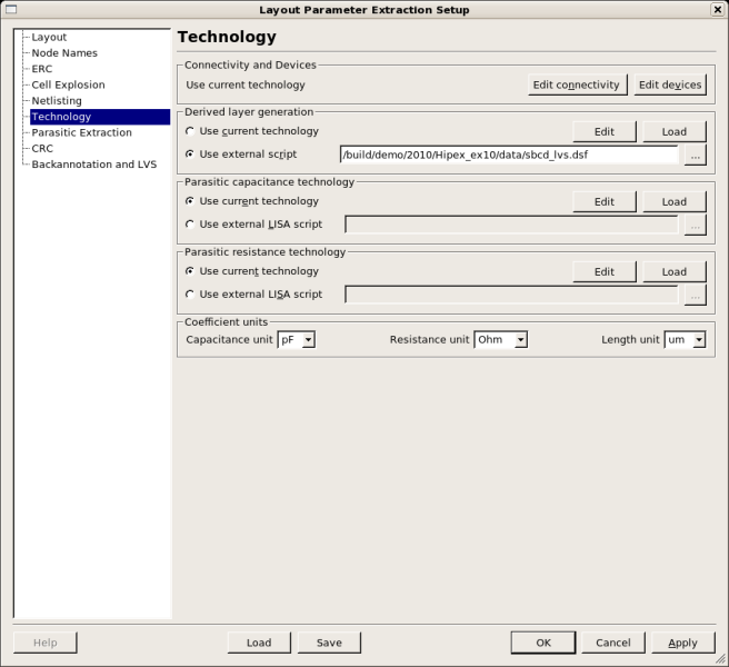
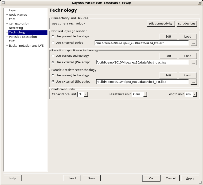
Select View->Toolbar->LPE to view the LPE Toolbar ( figure8 ). The LPE Toolbar provides access to the extraction setup and main extraction functions. To access the configuration controls, select LPE icon or Verification->Extraction->Setup. In the left-hand panel, click on the Technology menu ( figure9 ). In order for Hipex-NET to generate the netlist from the design layout it needs to have extracted the devices by first deriving the additional device layers. In the Derived layer generation section select Use external script . Use the [...] browser button to find the demo_sbcd_lvs.dsf layer derivation file. It should be found in .../10/techfiles/hipex. In a course of running Netlist Extraction, EXPERT will actually use the *_lvs.dsf script to generate (in the background) derived layers on the LNA_completed cell in the LNA.eld library, and output LNA_completed$HPX.gds file for Hipex-NET to perform the device and parasitic extractions on. The generated GDSII file will contain the original layout's data plus the device recognition derived layers.
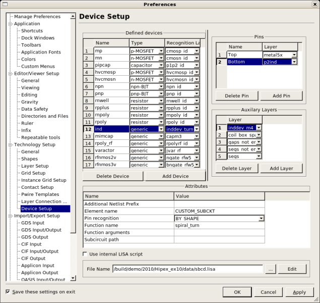
To configure generic devices for extraction, click on the Edit Devices button in Connectivity and Devices field to display the Device Setup screen ( figure10 ). Although the Generic devices are defined in the techfile the complex functions needed to calculate the equations based on the Auxiliary layers are defined in the LISA file, which must be configured within EXPERT. Hipex accesses these functions to evaluate any custom parameters needed to properly define a generic device. In the device, IND for example, custom parameters such as number of turns of the inductor coils or space between the turns are defined. The Auxiliary layers are created at the same time as all other derived layers.
2.2. Configuring Parasitic Extraction
The interlayer parasitic capacitances can be configured either using GUI or with use of LISA script. The latter way is chosen for presented example. In the Parasitic capacitance technology field of the LPE setup window ( figure11 ), select the Use LISA script file radio button and find the file demo_sbcd_dbc.lisa under .../10/techfiles/hipex.
Parasitic resistance parameters for this example are also defined with LISA script. In the Parasitic resistance technology field of the LPE setup window ( figure11 ), select the Use LISA script file radio button and find the file demo_sbcd_dbr.lisa under .../10/techfiles/hipex.
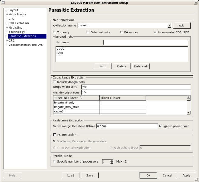
To provide further parasitic extraction tune-up, click Parasitic Extraction in the left panel of the LPE setup window. For presented example, the parasitic effects for some nets (power and ground) are not of particular interest; so they need to be eliminated from parasitic resistance and capacitance calculations: in the Ignored nets field, enter the names of the power and ground nets to be excluded from parasitic extraction. For example, type the net name "VDD2" and click on the Add button ( figure12 ). Similarly, add the net "gnd".
2.3. Configuring the Extraction Output
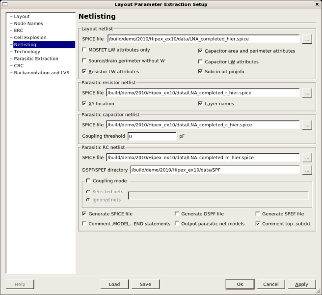
LPE can extract a variety of netlists. They can just be primary elements (*_hier.spice) or they can include parasitic elements, such as Rs and Cs (*_r_hier.spice, *_c_hier.spice, *_rc_hier.spice). These netlists can be created hierarchically or flat and can be separated, combined, or backannotated into another SPICE netlist. To see (and control) the Netlisting settings click on the Netlisting menu on the left-hand pane of the LPE Setup window. The Netlisting window will appear ( figure13 ). The file paths will obviously be different for your environment but the file names should be the same.
3.0 Running Netlist and Parasitic Extraction
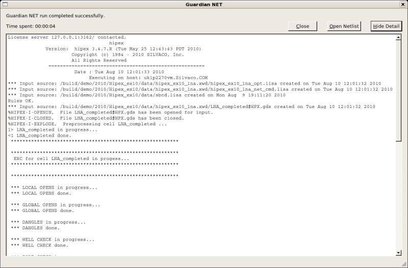
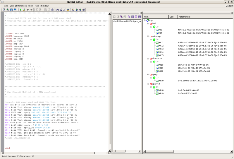
To perform the basic netlist extraction, press the NET icon on the LPE toolbar or select Verification->Extraction->Hipex Net->Run from menu. The details of the run will appear ( figure14 ) in new window. EXPERT generates the LNA_opt.lisa (LPE Setup fields in Hipex format) , LNA_net_cmd.lisa (Tech file device and layer info in Hipex format), and LNA_completed$HPX.gds (LNA_completed cell with derived layers from EXPERT in gds format) files for Hipex-NET to use (to generate the netlists required). Select Verification->Extraction->Hipex Net->View Hierarchical Netlist to see the extracted netlist for our LNA_completed cell ( figure15 ). The EXPERT Netlist Editor gives a clear view of both the layout netlist, LNA_completed_hier.spice and it's hierarchical device audit including the devices' layout parameters.
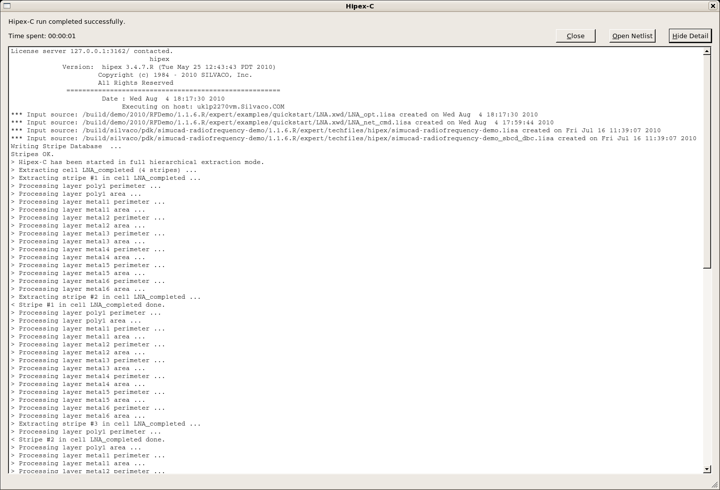
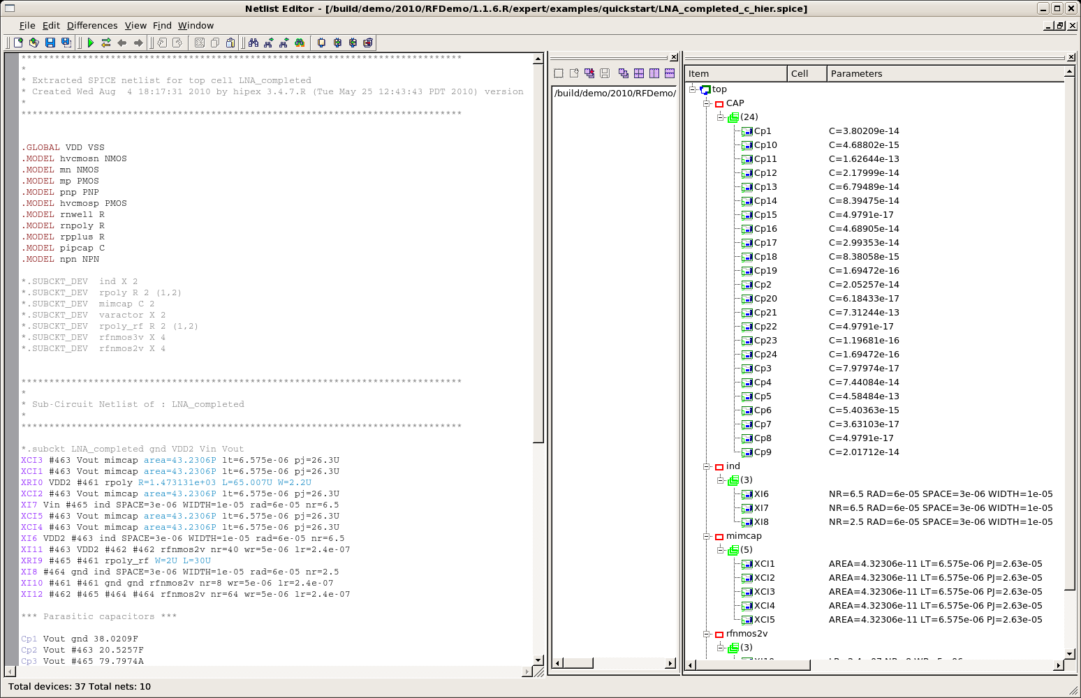
To perform the Hipex-C extraction, press C icon on the LPE toolbar or select Verification->Extraction->Hipex-C->Run. Figure16 shows the details of the run. Select Verification->Extraction->Hipex C->View Hierarchical Netlist to see the extracted netlist with parasitic capacitors included ( figure17 ). The Netlist Editor clearly shows the parasitic capacitors in it's audit.
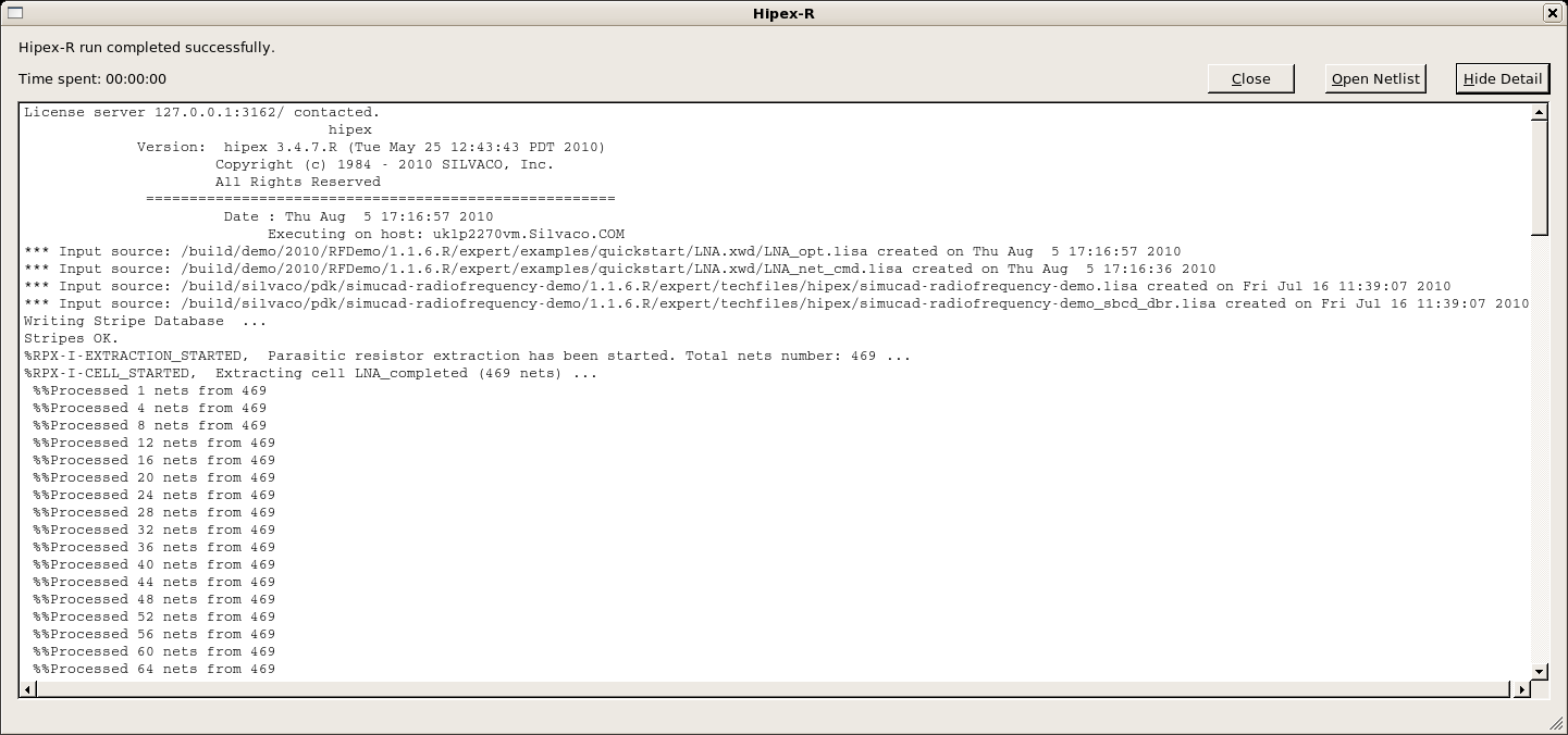
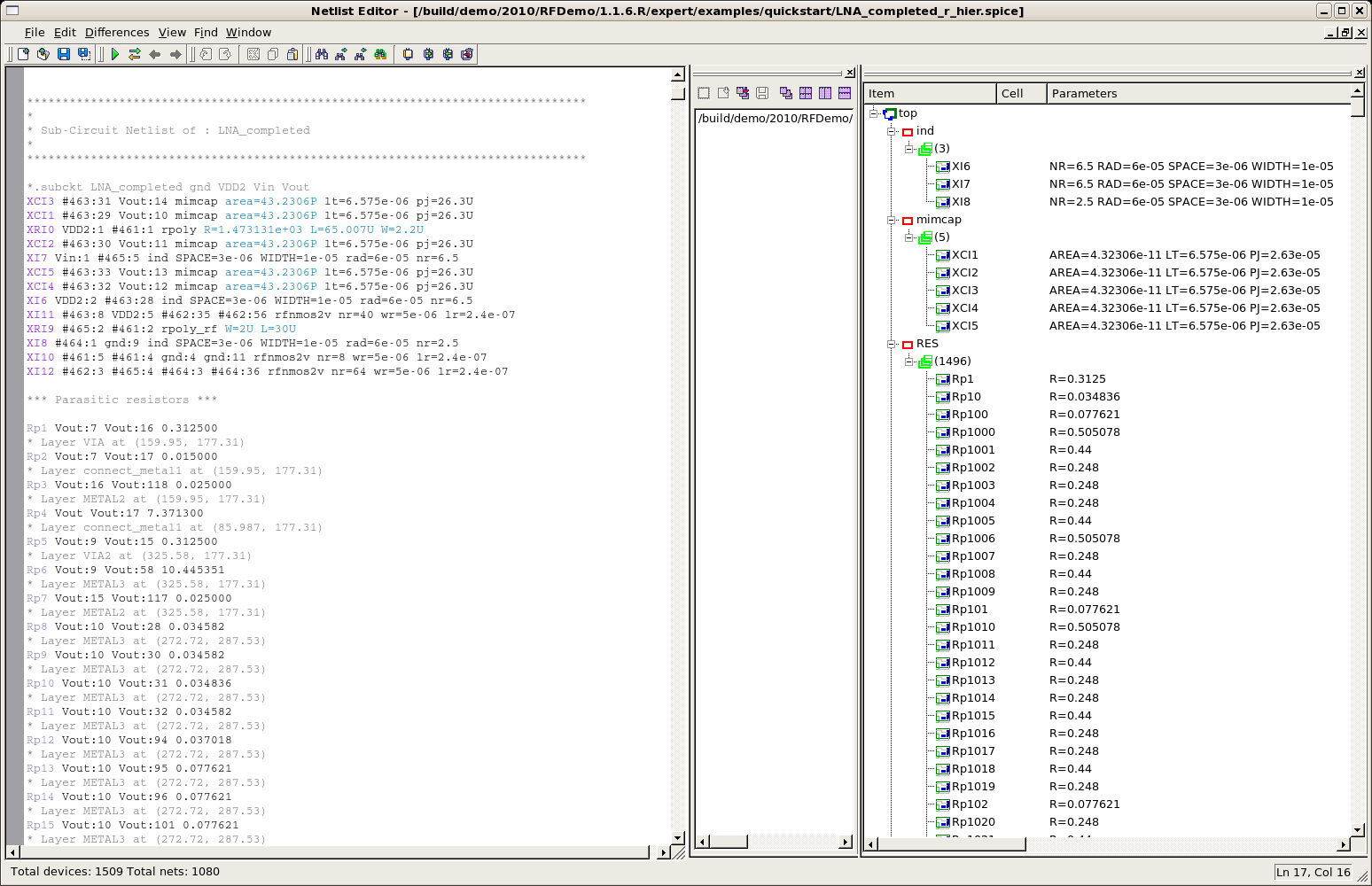
To perform the Hipex-R extraction, press R icon on the LPE toolbar or select Verification->Extraction->Hipex-R->Run. Figure18 shows the details of the run. Select Verification->Extraction->Hipex R->View Hierarchical Netlist to see the extracted netlist with parasitic resistors included ( figure19 ). The Netlist Editor clearly shows the parasitic resistors in it's audit.
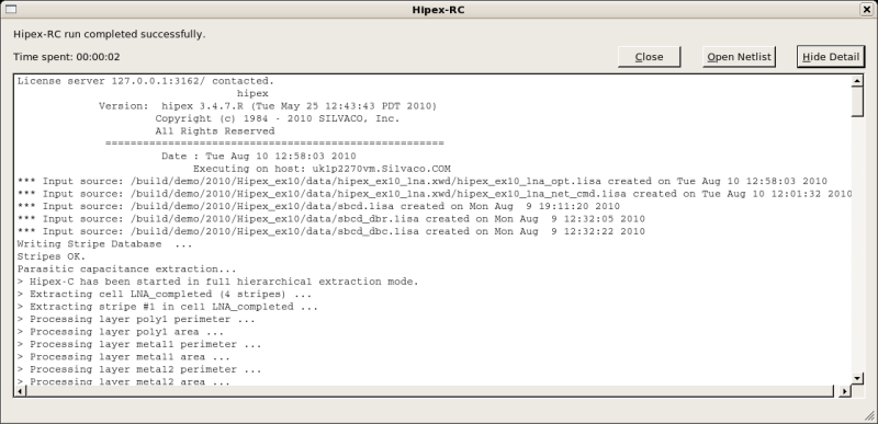
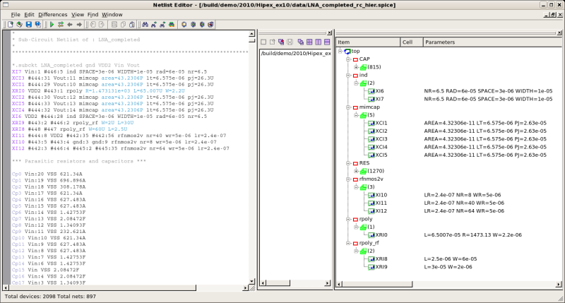
To perform the parasitic RC extraction, press RC icon on the LPE toolbar or select Verification->Extraction->Hipex-RC->Run. Figure20 shows the details of the run. Select Verification->Extraction->Hipex RC->View Hierarchical Netlist to see the extracted netlist with both parasitic resistors and capacitors ( figure21 ).
LNA_net_cmd.lisa
											!--------------------------------------------------------------------
!Net command file
!DESIGN    : design
!TECHNO    : techno
!USER      :
!TIME      : Thu May 28 20:07:44 2020

!--------------------------------------------------------------------

! HIPEX to CUP map table

cup layer "metal4" /hipex_layer="METAL4";
cup layer "metal6" /hipex_layer="METAL6";
cup layer "metal2" /hipex_layer="METAL2";
cup layer "metal3" /hipex_layer="METAL3";
cup layer "poly1" /hipex_layer="connect_poly";
cup layer "substrate" /hipex_layer="substrate";
cup layer "metal1" /hipex_layer="connect_metal1";
cup layer "metal5" /hipex_layer="metal5x";

! GDS LAYER MAP

hipex layer /gds_layer=   0 /gds_type= 0 /geom_layer="pnp_id";
hipex layer /gds_layer=  25 /gds_type= 0 /geom_layer="CONTACT";
hipex layer /gds_layer=  31 /gds_type= 0 /geom_layer="METAL4";
hipex layer /gds_layer=  31 /gds_type= 5 /geom_layer="METAL4_port";
hipex layer /gds_layer=  31 /gds_type= 6 /geom_layer="M4_port_text";
hipex layer /gds_layer=  32 /gds_type= 0 /geom_layer="VIA4";
hipex layer /gds_layer=  33 /gds_type= 5 /geom_layer="METAL5_port";
hipex layer /gds_layer=  33 /gds_type= 6 /geom_layer="M5_port_text";
hipex layer /gds_layer=  36 /gds_type= 0 /geom_layer="VIA5";
hipex layer /gds_layer=  37 /gds_type= 0 /geom_layer="METAL6";
hipex layer /gds_layer=  37 /gds_type= 6 /geom_layer="M6_port_text";
hipex layer /gds_layer=  38 /gds_type= 0 /geom_layer="DEEP_N_WELL";
hipex layer /gds_layer=  39 /gds_type= 0 /geom_layer="CTM3";
hipex layer /gds_layer=  42 /gds_type= 5 /geom_layer="NWEL_port";
hipex layer /gds_layer=  46 /gds_type= 5 /geom_layer="GC_port";
hipex layer /gds_layer=  49 /gds_type= 1 /text_layer="M1_LABEL";
hipex layer /gds_layer=  49 /gds_type= 5 /geom_layer="METAL1_port";
hipex layer /gds_layer=  49 /gds_type= 6 /text_layer="M1_port_text";
hipex layer /gds_layer=  50 /gds_type= 0 /geom_layer="VIA";
hipex layer /gds_layer=  51 /gds_type= 0 /geom_layer="METAL2";
hipex layer /gds_layer=  51 /gds_type= 5 /geom_layer="METAL2_port";
hipex layer /gds_layer=  51 /gds_type= 6 /geom_layer="M2_port_text";
hipex layer /gds_layer=  56 /gds_type= 0 /geom_layer="POLY2";
hipex layer /gds_layer=  59 /gds_type= 5 /geom_layer="PSUB_port";
hipex layer /gds_layer=  61 /gds_type= 0 /geom_layer="VIA2";
hipex layer /gds_layer=  62 /gds_type= 0 /geom_layer="METAL3";
hipex layer /gds_layer=  62 /gds_type= 5 /geom_layer="METAL3_port";
hipex layer /gds_layer=  62 /gds_type= 6 /geom_layer="M3_port_text";
hipex layer /gds_layer=  63 /gds_type= 0 /geom_layer="pnp_e";
hipex layer /gds_layer=  64 /gds_type= 0 /geom_layer="pnp_c";
hipex layer /gds_layer=  65 /gds_type= 0 /geom_layer="npn_e";
hipex layer /gds_layer=  66 /gds_type= 0 /geom_layer="npn_b";
hipex layer /gds_layer=  67 /gds_type= 0 /geom_layer="p_sd";
hipex layer /gds_layer=  68 /gds_type= 0 /geom_layer="n_sd";
hipex layer /gds_layer=  69 /gds_type= 0 /geom_layer="cmosp_id";
hipex layer /gds_layer=  70 /gds_type= 0 /geom_layer="cmosn_id";
hipex layer /gds_layer=  71 /gds_type= 0 /geom_layer="hvcmosp_id";
hipex layer /gds_layer=  72 /gds_type= 0 /geom_layer="hvpmos_d";
hipex layer /gds_layer=  73 /gds_type= 0 /geom_layer="hvpmos_s";
hipex layer /gds_layer=  74 /gds_type= 0 /geom_layer="hvcmosn_id";
hipex layer /gds_layer=  75 /gds_type= 0 /geom_layer="hvnmos_d";
hipex layer /gds_layer=  76 /gds_type= 0 /geom_layer="hvnmos_s";
hipex layer /gds_layer=  77 /gds_type= 0 /geom_layer="rpplus_id";
hipex layer /gds_layer=  78 /gds_type= 0 /geom_layer="rnpoly_id";
hipex layer /gds_layer=  79 /gds_type= 0 /geom_layer="rpoly_id";
hipex layer /gds_layer=  80 /gds_type= 0 /geom_layer="rnwell_id";
hipex layer /gds_layer=  81 /gds_type= 0 /geom_layer="rpplus_pin";
hipex layer /gds_layer=  82 /gds_type= 0 /geom_layer="connect_poly";
hipex layer /gds_layer=  83 /gds_type= 0 /geom_layer="connect_nwell";
hipex layer /gds_layer=  84 /gds_type= 0 /geom_layer="substrate";
hipex layer /gds_layer=  85 /gds_type= 0 /geom_layer="sub_tie";
hipex layer /gds_layer=  86 /gds_type= 0 /geom_layer="well_tie";
hipex layer /gds_layer=  87 /gds_type= 0 /geom_layer="p1p2_id";
hipex layer /gds_layer=  88 /gds_type= 0 /geom_layer="poly_con";
hipex layer /gds_layer=  89 /gds_type= 0 /geom_layer="poly2cap_con";
hipex layer /gds_layer=  90 /gds_type=255 /geom_layer="connect_metal1";
hipex layer /gds_layer=  91 /gds_type=255 /geom_layer="tv3";
hipex layer /gds_layer=  92 /gds_type=255 /geom_layer="cv3";
hipex layer /gds_layer=  93 /gds_type=255 /geom_layer="capm3";
hipex layer /gds_layer=  94 /gds_type=255 /geom_layer="metal5x";
hipex layer /gds_layer=  95 /gds_type=255 /geom_layer="p2ind";
hipex layer /gds_layer=  96 /gds_type=255 /geom_layer="segs";
hipex layer /gds_layer=  97 /gds_type=255 /geom_layer="gaps_not_end";
hipex layer /gds_layer=  98 /gds_type=255 /geom_layer="segs_not_end";
hipex layer /gds_layer=  99 /gds_type=255 /geom_layer="inddev_turn";
hipex layer /gds_layer= 100 /gds_type=255 /geom_layer="coil_box_space";
hipex layer /gds_layer= 101 /gds_type=255 /geom_layer="inddev_m4";
hipex layer /gds_layer= 102 /gds_type=255 /geom_layer="rpolyrf_id";
hipex layer /gds_layer= 103 /gds_type=255 /geom_layer="L_edge_pres_rf";
hipex layer /gds_layer= 104 /gds_type=255 /geom_layer="jvar_rf";
hipex layer /gds_layer= 105 /gds_type=255 /geom_layer="jvar3_rf";
hipex layer /gds_layer= 106 /gds_type=255 /geom_layer="ngate_rfw5_nthin";
hipex layer /gds_layer= 107 /gds_type=255 /geom_layer="ngate_rfw5";
hipex layer /gds_layer= 108 /gds_type=255 /geom_layer="s_ndiff";
hipex layer /gds_layer= 109 /gds_type=255 /geom_layer="d_ndiff";
hipex layer /gds_layer= 110 /gds_type=255 /geom_layer="ngate_rf_poly";
hipex layer /gds_layer= 111 /gds_type=255 /geom_layer="bngate_rfw5_nthin";
hipex layer /gds_layer= 112 /gds_type=255 /geom_layer="bngate_rfw5";
hipex layer /gds_layer= 113 /gds_type=255 /geom_layer="s_bndiff";
hipex layer /gds_layer= 114 /gds_type=255 /geom_layer="d_bndiff";
hipex layer /gds_layer= 115 /gds_type=255 /geom_layer="bngate_rf_poly";
hipex layer /gds_layer= 116 /gds_type=255 /geom_layer="ngate_rf_sw";
hipex layer /gds_layer= 117 /gds_type=255 /geom_layer="ngate_rf_dw";
hipex layer /gds_layer= 118 /gds_type=255 /geom_layer="bngate_rf_sw";
hipex layer /gds_layer= 119 /gds_type=255 /geom_layer="bngate_rf_dw";
hipex layer /gds_layer= 120 /gds_type=255 /geom_layer="hvnmos_body";
hipex layer /gds_layer= 121 /gds_type=255 /geom_layer="hvnmos_wellbody";
hipex layer /gds_layer= 122 /gds_type=255 /geom_layer="npn_pbase";
hipex layer /gds_layer= 123 /gds_type=255 /geom_layer="dnwc";
hipex layer /gds_layer= 124 /gds_type=255 /geom_layer="npn_id";

! TEXT TYPES


! PORT LAYERS

hipex port_layer "M1_port_text";

! SOFT LAYERS

hipex soft_layer "DEEP_N_WELL" /link="";
hipex soft_layer "NWEL_port" /link="";
hipex soft_layer "PSUB_port" /link="";
hipex soft_layer "connect_nwell" /link="";
hipex soft_layer "dnwc" /link="";
hipex soft_layer "substrate" /link="";

! MISC (optional) statementsS


! CONNECTIVITY

hipex connect "METAL2" "METAL2_port";
hipex connect "METAL2" "METAL3" /contact="VIA2";
hipex connect "METAL3" "METAL3_port";
hipex connect "METAL3" "METAL4" /contact="tv3";
hipex connect "METAL4" "CTM3" /contact="cv3";
hipex connect "METAL4" "METAL4_port";
hipex connect "METAL4" "metal5x" /contact="VIA4";
hipex connect "bngate_rf_poly";
hipex connect "connect_metal1" "POLY2" /contact="poly2cap_con";
hipex connect "connect_metal1" "METAL1_port";
hipex connect "connect_metal1" "METAL2" /contact="VIA";
hipex connect "connect_metal1" "pnp_e" /contact="CONTACT";
hipex connect "connect_metal1" "pnp_c" /contact="CONTACT";
hipex connect "connect_metal1" "npn_e" /contact="CONTACT";
hipex connect "connect_metal1" "npn_b" /contact="CONTACT";
hipex connect "connect_metal1" "p_sd" /contact="CONTACT";
hipex connect "connect_metal1" "n_sd" /contact="CONTACT";
hipex connect "connect_metal1" "hvpmos_d" /contact="CONTACT";
hipex connect "connect_metal1" "hvpmos_s" /contact="CONTACT";
hipex connect "connect_metal1" "hvnmos_d" /contact="CONTACT";
hipex connect "connect_metal1" "hvnmos_s" /contact="CONTACT";
hipex connect "connect_metal1" "rpplus_pin" /contact="CONTACT";
hipex connect "connect_metal1" "connect_poly" /contact="poly_con";
hipex connect "connect_metal1" "sub_tie" /contact="CONTACT";
hipex connect "connect_metal1" "well_tie" /contact="CONTACT";
hipex connect "connect_metal1" "s_ndiff" /contact="CONTACT";
hipex connect "connect_metal1" "d_ndiff" /contact="CONTACT";
hipex connect "connect_metal1" "s_bndiff" /contact="CONTACT";
hipex connect "connect_metal1" "d_bndiff" /contact="CONTACT";
hipex connect "connect_metal1" "hvnmos_body" /contact="CONTACT";
hipex attach "M1_port_text" "connect_metal1";
hipex attach "M1_LABEL" "connect_metal1";
hipex connect "connect_nwell" "NWEL_port";
hipex connect "connect_nwell" "DEEP_N_WELL" /contact="dnwc";
hipex connect "connect_nwell" "well_tie";
hipex connect "connect_poly" "GC_port";
hipex connect "connect_poly" "ngate_rf_poly";
hipex connect "connect_poly" "bngate_rf_poly";
hipex connect "hvnmos_wellbody" "hvnmos_body";
hipex connect "metal5x" "METAL5_port";
hipex connect "metal5x" "METAL6" /contact="VIA5";
hipex connect "metal5x" "p2ind";
hipex connect "ngate_rf_poly";
hipex connect "npn_pbase" "npn_b";
hipex connect "p2ind";
hipex connect "substrate" "PSUB_port";
hipex connect "substrate" "sub_tie";

! DEVICES TEXTS


! DEVICE DEFINITIONS

hipex define_device PMOS "cmosp_id" /drain="p_sd" /gate="connect_poly" /source="p_sd" /subs="connect_nwell" /model_name="mp";
hipex define_device NMOS "cmosn_id" /drain="n_sd" /gate="connect_poly" /source="n_sd" /subs="substrate" /model_name="mn";
hipex define_device C "p1p2_id" /pin1="POLY2" /pin2="connect_poly" /area_cap=0.0075 /perim_cap=0.00925 /model_name="pipcap";
hipex define_device PMOS "hvcmosp_id" /drain="hvpmos_d" /gate="connect_poly" /source="hvpmos_s" /subs="DEEP_N_WELL" /model_name="hvcmosp";
hipex define_device NMOS "hvcmosn_id" /drain="hvnmos_d" /gate="connect_poly" /source="hvnmos_s" /subs="hvnmos_wellbody" /model_name="hvcmosn";
hipex define_device NPN "npn_id" /collector="connect_nwell" /base="npn_pbase" /emitter="npn_e" /subs="substrate" /area_unit=36 /model_name="npn";
hipex define_device PNP "pnp_id" /collector="pnp_c" /base="connect_nwell" /emitter="pnp_e" /area_unit=38.3819 /model_name="pnp";
hipex define_device R "rnwell_id" /pin1="connect_nwell" /pin2="connect_nwell" /subs="substrate" /cont_res=0 /delta_l=0.4 /delta_w=-0.02 /head_res=0 /sheet_res=10000 /model_name="rnwell";
hipex define_device R "rpplus_id" /pin1="rpplus_pin" /pin2="rpplus_pin" /subs="connect_nwell" /cont_res=0 /delta_l=0.5 /delta_w=-0.05 /head_res=0 /sheet_res=200 /model_name="rpplus";
hipex define_device R "rnpoly_id" /pin1="connect_poly" /pin2="connect_poly" /cont_res=0 /delta_l=0.4 /delta_w=0.02 /head_res=0 /sheet_res=50 /model_name="rnpoly";
hipex define_device R "rpoly_id" /pin1="connect_poly" /pin2="connect_poly" /cont_res=0 /delta_l=0.4 /delta_w=0.02 /head_res=0 /sheet_res=50 /model_name="rpoly" /netlist_prefix="X";
hipex generic_device "inddev_turn" /pins=({{"metal5x", "Top"}, {"p2ind", "Bottom"}}) /auxs={"inddev_m4", "coil_box_space", "gaps_not_end", "segs_not_end", "segs"} /by_shape /func="spiral_turn" /element_name="CUSTOM_SUBCKT" /subckt_filename="" /model_name="ind";
hipex generic_device "capm3" /pins=({{"CTM3", "Pos"}, {"METAL3", "Neg"}}) /by_shape /func="mimcap" /element_name="C" /model_name="mimcap" /netlist_prefix="X";
hipex generic_device "rpolyrf_id" /pins=({{"connect_poly", "Pos"}, {"connect_poly", "Neg"}}) /auxs={"L_edge_pres_rf"} /by_shape /func="rpolyrf" /element_name="R" /model_name="rpoly_rf" /netlist_prefix="X";
hipex generic_device "jvar_rf" /pins=({{"p_sd", "A"}, {"well_tie", "K"}}) /auxs={"jvar3_rf"} /by_net /func="varactor" /element_name="CUSTOM_SUBCKT" /subckt_filename="" /model_name="varactor";
hipex generic_device "ngate_rfw5_nthin" /pins=({{"d_ndiff", "D"}, {"ngate_rf_poly", "G"}, {"s_ndiff", "S"}, {"substrate", "SUB"}}) /auxs={"ngate_rfw5", "ngate_rf_dw", "ngate_rf_sw"} /by_shape /func="rfnmos2v" /element_name="CUSTOM_SUBCKT" /subckt_filename="" /model_name="rfnmos2v";
hipex generic_device "bngate_rfw5_nthin" /pins=({{"d_bndiff", "D"}, {"bngate_rf_poly", "G"}, {"s_bndiff", "S"}, {"substrate", "SUB"}}) /auxs={"bngate_rfw5", "bngate_rf_dw", "bngate_rf_sw"} /by_shape /func="rfnmos3v" /element_name="CUSTOM_SUBCKT" /subckt_filename="" /model_name="rfnmos3v";
Include("/home/alexa/2020_06/10/techfiles/hipex/simucad-radiofrequency-demo.lisa");

! SOFT/WELL CHECKS

hipex soft_check "DEEP_N_WELL";
hipex soft_check "connect_nwell";
hipex soft_check "dnwc";
hipex soft_check "substrate";

! MASKED DIELECTRIC LAYERS
LNA_opt.lisa
											!--------------------------------------------------------------------
!Run file
!DESIGN    : design
!TECHNO    : techno
!USER      :
!TIME      : Thu May 28 20:08:16 2020

!--------------------------------------------------------------------
TOP_CELL                                = "LNA_completed";

HIPEX_DB_DIRECTORY                      = "database";
!--------------------------------------------------------------------
!Extraction: LISA template command file
!--------------------------------------------------------------------

!--------------------------------------------------------------------
!Layout parameters
!--------------------------------------------------------------------
HIPEX_LAYOUT_FORMAT                     = "GDS";
HIPEX_LAYOUT_FILE                       = "LNA_completed$HPX.gds";
HIPEX_OVERLAP_INSTANCE_CHECK            = "NO";
HIPEX_SUPPRESS_NOTEMPTY                 = "YES";
HIPEX_NON45_FLAG                        = "NO";

!--------------------------------------------------------------------
!Connectivity parameters
!--------------------------------------------------------------------
HIPEX_TERNARY_CONNECT_THROUGH_TOUCH     = "NO";

!--------------------------------------------------------------------
!Output parameters
!--------------------------------------------------------------------
HIPEX_COMMENT_MODEL                     = "NO";
HIPEX_COMMENT_TOP_SUBCKT                = "NO";
HIPEX_HIER_SPICE_WL_NAME                = "/home/alexa/2020_06/10/LNA_completed_hier.spice";
HIPEX_MOSFET_LW_ONLY                    = "NO";
HIPEX_MOSFET_EXCLUDE_W_SD               = "NO";
HIPEX_OUTPUT_SPICE_ATTRIBUTES           = "YES";
HIPEX_CAP_OUTPUT_LW                     = "NO";
HIPEX_RES_OUTPUT_LW                     = "YES";
HIPEX_CAP_OUTPUT_AREA_PERIMETER         = "YES";
HIPEX_OUTPUT_SPICE_FORMAT               = "HSPICE";
HIPEX_PININFO                           = "NO";
HIPEX_PRINT_MESSAGES                    = "NO";
NETLIST_OUTPUT_PM                       = "NO";
NETLIST_DISTRIBUTION_MODE               = "ACCURATE";
NETLIST_LINE_LENGTH                     = 80;
NETLIST_EXCLUDE_LIBRARY_PREFIX          = "NO";
NETLIST_GLOBALS_IN_SUBCKT_PINS          = "YES";
NETLIST_TEXTED_PINS                     = "YES";
NETLIST_LIBRARIES                       = {"simucad_demo_pcells"};

!--------------------------------------------------------------------
!ERC parameters
!--------------------------------------------------------------------
HIPEX_DANGLE_FLAG                       = "YES";
HIPEX_CAP_MESSAGE                       = "YES";
HIPEX_DIODE_MESSAGE                     = "NO";
HIPEX_RENAME_OPENS                      = "YES";
HIPEX_MULTILABEL_NAME                   = "";
HIPEX_SOFTCHECK_WARNINGS_AS_ERRORS      = "NO";

!--------------------------------------------------------------------
!Node Name parameters
!--------------------------------------------------------------------
HIPEX_HIERARCHY_SEPARATOR               = "/";
HIPEX_NODE_NAME_SEPARATOR               = "_";
HIPEX_DEFAULT_INSTANCE_PREFIX           = "I";
HIPEX_DEFAULT_NODE_PREFIX               = "#";
HIPEX_DELETE_BAD_CHAR                   = "NO";
HIPEX_XY_LOCATION                       = "NO";
HIPEX_CASE_SENSITIVE_NET_NAMES          = "YES";
HIPEX_AUTOGENERATE_LOCAL                = "YES";
POWER_NODE                              = {"VDD2"};
GROUND_NODE                             = {"gnd"};
GLOBAL_TEXT_LIST                        = {"VDD2", "gnd"};
HIPEX_PIN_DELIMITER                     = ":";

!--------------------------------------------------------------------
!Explosion parameters
!--------------------------------------------------------------------
HIPEX_WIRING_EXPLODE                    = "NO";
HIPEX_KEEP_FLATTEN_CELLS                = "YES";
HIPEX_TEXT_TOP                          = "NO";
HIPEX_AUTO_EXPLODE                      = "NO";
HIPEX SET_CELL_OPTIONS {"simucad_demo_pcells_contact_box_1_2.4_7hl2sk"} /EXPLODE;
HIPEX SET_CELL_OPTIONS {"simucad_demo_pcells_rppoly_2.2_65.007_895vg1"} /EXPLODE;
HIPEX SET_CELL_OPTIONS {"{CONTACT}_M1_ACT_3000_10_10_8000_8000_4_0_1_30000"} /EXPLODE;
HIPEX SET_CELL_OPTIONS {"simucad_demo_pcells_via23_box_9.92_2.9_0.4_0.5_30wzgj"} /EXPLODE;
HIPEX SET_CELL_OPTIONS {"simucad_demo_pcells_via23_box_83.36_2_0.4_0.5_txd6i8"} /EXPLODE;
HIPEX SET_CELL_OPTIONS {"simucad_demo_pcells_via23_box_79.36_2.9_0.4_0_wb6184"} /EXPLODE;
HIPEX SET_CELL_OPTIONS {"simucad_demo_pcells_via23_box_53.6_2_0.4_0.5_bwzuq8"} /EXPLODE;
HIPEX SET_CELL_OPTIONS {"simucad_demo_pcells_via23_box_49.6_2.9_0.4_0.5_1muxeq"} /EXPLODE;
HIPEX SET_CELL_OPTIONS {"simucad_demo_pcells_via23_box_13.92_2_0.4_0.5_tld9gf"} /EXPLODE;
HIPEX SET_CELL_OPTIONS {"simucad_demo_pcells_via23_box_1.5_14.9_0.4_0.5_g2mkbw"} /EXPLODE;
HIPEX SET_CELL_OPTIONS {"simucad_demo_pcells_via23_box_0.4_3.7_0.4_0.5_d2z7zu"} /EXPLODE;
HIPEX SET_CELL_OPTIONS {"simucad_demo_pcells_via1_box_83.36_2_voy0uh"} /EXPLODE;
HIPEX SET_CELL_OPTIONS {"simucad_demo_pcells_via1_box_53.6_2_p2mjix"} /EXPLODE;
HIPEX SET_CELL_OPTIONS {"simucad_demo_pcells_via1_box_13.92_2_c9w8u0"} /EXPLODE;
HIPEX SET_CELL_OPTIONS {"simucad_demo_pcells_via1_box_1.5_14.9_uo94dx"} /EXPLODE;
HIPEX SET_CELL_OPTIONS {"simucad_demo_pcells_via1_box_0.4_3.7_sletoz"} /EXPLODE;
HIPEX SET_CELL_OPTIONS {"simucad_demo_pcells_contact_box_0.3_4.3_pgl1pl"} /EXPLODE;
HIPEX SET_CELL_OPTIONS {"simucad_demo_pcells_rfnmos2v_5_0.24_8_OFF_xz4cdv"} /EXPLODE;
HIPEX SET_CELL_OPTIONS {"simucad_demo_pcells_rfnmos2v_5_0.24_64_OFF_fs1ixv"} /EXPLODE;
HIPEX SET_CELL_OPTIONS {"simucad_demo_pcells_rfnmos2v_5_0.24_40_OFF_ymvixt"} /EXPLODE;
HIPEX SET_CELL_OPTIONS {"{CONTACT}_M4_M5_10000_1_1_20000_20000_4_0_1_100000"} /EXPLODE;
HIPEX SET_CELL_OPTIONS {"{CONTACT}_M3_M4_4000_1_1_9000_9000_4_0_1_40000"} /EXPLODE;
HIPEX SET_CELL_OPTIONS {"{CONTACT}_M2_M3_4000_1_1_9000_9000_4_0_1_40000"} /EXPLODE;
HIPEX SET_CELL_OPTIONS {"simucad_demo_pcells_contact_box_0.8_2.4_cvewod"} /EXPLODE;
HIPEX SET_CELL_OPTIONS {"simucad_demo_pcells_rppoly_rf_2_30_t6595i"} /EXPLODE;
HIPEX SET_CELL_OPTIONS {"simucad_demo_pcells_via45_box_8_8_1_1_o680tp"} /EXPLODE;
HIPEX SET_CELL_OPTIONS {"simucad_demo_pcells_ind_prim_65_6.5_10_3_4rdcid"} /EXPLODE;
HIPEX SET_CELL_OPTIONS {"simucad_demo_pcells_ind_prim_65_2.5_10_3_1cqsux"} /EXPLODE;
HIPEX SET_CELL_OPTIONS {"simucad_demo_pcells_ind_60_6.5_10_3_tyfmsa"} /EXPLODE;
HIPEX SET_CELL_OPTIONS {"simucad_demo_pcells_ind_60_2.5_10_3_qjt34u"} /EXPLODE;
HIPEX SET_CELL_OPTIONS {"{CONTACT}_M1_M2_4000_1_1_9000_9000_4_0_1_40000"} /EXPLODE;
HIPEX SET_CELL_OPTIONS {"{CONTACT}_M2_M3_4000_1_1_50000_50000_4_0_1_40000"} /EXPLODE;
HIPEX SET_CELL_OPTIONS {"{CONTACT}_M3_M4_4000_1_1_50000_50000_4_0_1_40000"} /EXPLODE;
HIPEX SET_CELL_OPTIONS {"simucad_demo_pcells_via34_box_3.575_3.575_0.4_6mqtrs"} /EXPLODE;
HIPEX SET_CELL_OPTIONS {"simucad_demo_pcells_mimcap_0_CAP_400_6.5728_O_opczvs"} /EXPLODE;
HIPEX SET_CELL_OPTIONS {"LNA_completed"} /EXPLODE;

!--------------------------------------------------------------------
!Pins parameters
!--------------------------------------------------------------------
HIPEX_IGNORE_DANGLE_PINS                = "YES";

!--------------------------------------------------------------------
!Virtual Nets parameters
!--------------------------------------------------------------------
HIPEX_CHANGE_VIRTUAL_NETS               = "SUFFIX";
HIPEX_VIRTUAL_NET_SYMBOLS               = ":";
HIPEX_TOP_VIRTUAL_CONNECT_ONLY          = "YES";

!--------------------------------------------------------------------
!BackAnnotate parameters
!--------------------------------------------------------------------
HIPEX_BACKANNOTATE                      = "NO";

!--------------------------------------------------------------------
!Capacitance Extraction parameters
!--------------------------------------------------------------------
CPX_COUPLED_THRESHOLD                   = 0.0;
CPX_EXTRACT_DANGLES                     = "NO";
CPX_OUTPUT_DUMMY_CAPA                   = "NO";
CPX_FIELD_SOLVER                        = "NO";

!--------------------------------------------------------------------
!Field Solver C-extraction (Stellar) parameters
!--------------------------------------------------------------------
CPX_STEP_X                              = 0.5;
CPX_STEP_Y                              = 0.5;
CPX_STEP_Z                              = 0.5;
CPX_PRECISION                           = 0.01;
CPX_MAX_ITER                            = 100;
CPX_DECOMPOSITION                       = "YES";
CPX_DEC_STEP                            = "NO";
CPX_DEC_VALUE                           = -1.0;
CPX_BOX                                 = "NO";
CPX_BOX_VALUES_XMIN                     = 0.0;
CPX_BOX_VALUES_XMAX                     = 0.0;
CPX_BOX_VALUES_YMIN                     = 0.0;
CPX_BOX_VALUES_YMAX                     = 0.0;
CPX_FILTER                              = "NO";
CPX_CAPA_MIN                            = 1e-20;
CPX_RENEW                               = "NO";
CPX_SAVE_FILE                           = "/home/alexa/2020_06/10/RenewSavedFile.sav";
CPX_THREED_GENERATION                   = "NO";
CPX_THREED_FILENAME                     = "/home/alexa/2020_06/10/3DStructureFile.str";

!--------------------------------------------------------------------
!Field Solver C-extraction (Clever) parameters
!--------------------------------------------------------------------

!--------------------------------------------------------------------
!Resistance Extraction parameters
!--------------------------------------------------------------------
RPX_SERIAL_MERGE_THRESHOLD              = 0.0;
RPX_OUTPUT_XY                           = "NO";
RPX_OUTPUT_LAYER_NAMES                  = "NO";
RPX_SKIP_POWER                          = "YES";
RPX_USE_TEXTS_AS_SUBNODES               = "NO";
RPX_USE_FIELD_SOLVER                    = "NO";

!--------------------------------------------------------------------
!Netlist RC Reduction parameters
!--------------------------------------------------------------------
NETLIST_CRC                             = "NO";

!--------------------------------------------------------------------
!Coefficient Units parameters
!--------------------------------------------------------------------
HIPEX SET_UNIT /CAPACITANCE "pF";
HIPEX SET_UNIT /RESISTANCE "Ohm";
HIPEX SET_UNIT /LENGTH "um";
run_c.lisa
											INCLUDE ("LNA_opt.lisa");
INCLUDE ("LNA_net_cmd.lisa");
INCLUDE ("/home/alexa/2020_06/10/techfiles/hipex/demo_sbcd_dbc.lisa");

HIPEX_SUMMARY_PATH                      = "/home/alexa/2020_06/10";
HDB READ;
print("Writing Stripe Database  ...");
HDB WRITE_STRIPES /FULL/IGNORE/NETS="VDD*","GND*","VSS*" "default" 200 10;
print("Stripes OK.");
CPX MAIN "default" /rewrite;
netlist spice/hier/c "/home/alexa/2020_06/10/LNA_completed_c_hier.spice";
run_net.lisa
											INCLUDE ("LNA_opt.lisa");
INCLUDE ("LNA_net_cmd.lisa");

HIPEX_SUMMARY_PATH                      = "/home/alexa/2020_06/10";
HIPEX_NET_MAIN();
run_rc.lisa
											INCLUDE ("LNA_opt.lisa");
INCLUDE ("LNA_net_cmd.lisa");
INCLUDE ("/home/alexa/2020_06/10/techfiles/hipex/demo_sbcd_dbr.lisa");
INCLUDE ("/home/alexa/2020_06/10/techfiles/hipex/demo_sbcd_dbc.lisa");

HIPEX_SUMMARY_PATH                      = "/home/alexa/2020_06/10";
HDB READ;
print("Writing Stripe Database  ...");
HDB WRITE_STRIPES /FULL "default" 200 10;
print("Stripes OK.");
print("Parasitic capacitance extraction...");
CPX MAIN "default" /rewrite;
print("Parasitic resistance extraction...");
RPX MAIN "default" /rewrite;
netlist spice/hier/rcc  "/home/alexa/2020_06/10/LNA_completed_rc_hier.spice";
run_r.lisa
											INCLUDE ("LNA_opt.lisa");
INCLUDE ("LNA_net_cmd.lisa");
INCLUDE ("/home/alexa/2020_06/10/techfiles/hipex/demo_sbcd_dbr.lisa");

HIPEX_SUMMARY_PATH                      = "/home/alexa/2020_06/10";
HDB READ;
print("Writing Stripe Database  ...");
HDB WRITE_STRIPES /FULL/IGNORE/NETS="VDD*","GND*","VSS*" "default" 200 10;
print("Stripes OK.");
RPX MAIN "default" /rewrite;
netlist spice/hier/r "/home/alexa/2020_06/10/LNA_completed_r_hier.spice";
demo_sbcd_drc.dsf
											Update_layout: input=no, technology=no, new=no;
output_error_subsegments: yes;
Merge_Input: on;
////////////////////
// Global Defines //
////////////////////
Substrate: LayerR=&A;
Logicform: PSUB=&A.dif.(N_WELL.or.DEEP_N_WELL);
Logicform: Nactive_in_PWELL=(N_PLUS_SELECT.and.ACTIVE.and.PSUB);
Logicform: ISOPWELL=DEEP_N_WELL.dif.N_WELL;
Logicform: Nactive_in_ISOPWELL=(N_PLUS_SELECT.and.ACTIVE.and.ISOPWELL);
Logicform: Pactive_in_NWELL=P_PLUS_SELECT.and.ACTIVE.and.N_WELL;
Logicform: NWELL_TIE=N_PLUS_SELECT.and.ACTIVE.AND.N_WELL;
Logicform: PSUB_TIE=(P_PLUS_SELECT.and.ACTIVE).DIF.N_WELL;
Logicform: SD_ACTIVE=(P_PLUS_SELECT.and.ACTIVE.AND.N_WELL).or.((N_PLUS_SELECT.and.ACTIVE).DIF.N_WELL);
Logicform: SUB_TIE_ACTIVE=(NWELL_TIE).or.(PSUB_TIE);
//////////////////////////
// Connectivity Defines //
//////////////////////////
Connect: Layer1=N_WELL, Layer2=NWELL_TIE ,LayerC=CONTACT, Options =(I-);
Connect: Layer1=PSUB, Layer2=PSUB_TIE ,LayerC=CONTACT, Options =(I-);
///////////////////
//Rules for N_WELL
///////////////////
//1.1  Minimum width
Select: Relation=overlap, Layer1=N_WELL, layer2=THICK_ACTIVE, LayerR=REG_NWELL, Options=(not);
Width: Layer = REG_NWELL, Limits<5, ID= "1.1  Minimum width";
//1.2  Minimum spacing between wells at different potential
OutDistance: Layer = N_WELL, Limits<5 , Options=(C), ID= "1.2  Minimum spacing between wells at different potential";
//1.3  Minimum spacing between wells at same potential
OutDistance: Layer = N_WELL, Limits<6, Options=(N,C'), ID= "1.3  Minimum spacing between wells at same potential";
//1.4  Minimum spacing between wells of different type (if both are drawn)
Logicform: OVERLAPPING_WELLS=(N_WELL).and.(P_WELL);
Copy: Layer=OVERLAPPING_WELLS,  ID="1.4  Minimum spacing between wells of different type (if both are drawn)";
///////////////////
//Rules for ACTIVE
///////////////////
//2.1  Minimum width
Width: Layer = ACTIVE, Limits<0.58  , ID= "2.1  Minimum width";
//2.2  Minimum spacing
OutDistance: Layer = ACTIVE, Limits<1  , Options=(N), ID= "2.2  Minimum spacing";
//2.3  Source/drain active to well edge

InDistance: Layer1 = SD_ACTIVE, Layer2 = REG_NWELL, Limits<2  , Options=(T), ID="2.3  Source/drain active to well edge";
OutDistance: Layer1 = SD_ACTIVE, Layer2 = REG_NWELL, Limits<2  , Options=(T), ID="2.3  Source/drain active to well edge";
//2.4  Substrate/well contact active to well edge
InDistance: Layer1 = SUB_TIE_ACTIVE, Layer2 = REG_NWELL, Limits<1  , Options=(T), ID="2.4  Substrate/well contact active to well edge";
OutDistance: Layer1 = SUB_TIE_ACTIVE, Layer2 = REG_NWELL, Limits<1  , Options=(T), ID="2.4  Substrate/well contact active to well edge";
//2.5  Minimum spacing between non-abutting active of different implant. Abutting active ("split-active") is illustrated under Select Layout Rules.
Select: Layer1=P_PLUS_SELECT, Layer2=N_PLUS_SELECT, LayerR=PtouchN, relation=touch;
Select: Layer1=N_PLUS_SELECT, Layer2=P_PLUS_SELECT, LayerR=NtouchP, relation=touch;
Logicform: naaodi=(PtouchN.or.NtouchP).and.ACTIVE;
OutDistance: Layer = naaodi, Limits<2, Options=(N), ID= "2.5  Minimum spacing between non-abutting active of different implant. Abutting active (split-active) is illustrated under Select Layout Rules.";
///////////////////
//Rules for POLY
///////////////////
Logicform: TRANSISTOR=(POLY.and.ACTIVE);
//3.1  Minimum width
Width: Layer = POLY, Limits<0.24  , ID= "3.1  Minimum width";
//3.2  Minimum spacing over field
Logicform: FIELDPOLY=POLY.DIF.ACTIVE;
OutDistance: Layer = FIELDPOLY, Limits<1  , Options=(N), ID= "3.2  Minimum spacing over field";
//3.2.a  Minimum spacing over active
OutDistance: Layer = TRANSISTOR, Limits<1, Options=(N), ID= "3.2.a  Minimum spacing over active";
//3.3  Minimum gate extension of active
InDistance: Layer1 = TRANSISTOR, Layer2 = POLY, Limits<0.5, ID="3.3  Minimum gate extension of active";
//3.4  Minimum active extension of poly
InDistance: Layer1 = TRANSISTOR, Layer2 = ACTIVE, Limits<1, ID="3.4  Minimum active extension of poly";
//3.5  Minimum field poly to active
OutDistance: Layer1=POLY, Layer2=ACTIVE, Limits<0.4 , Options=(T), ID="3.5  Minimum field poly to active";
///////////////////
//Rules for N_PLUS_SELECT
///////////////////
Logicform: SELECT=N_PLUS_SELECT.or.P_PLUS_SELECT;
//4.1  Minimum select spacing to channel of transistor to ensure adequate source/drain width
OutDistance: Layer1 = TRANSISTOR, Layer2 = SUB_TIE_ACTIVE, Limits<1, ID= "4.1  Minimum select spacing to channel of transistor";
//4.2  Minimum select overlap of active
InDistance: Layer1 = ACTIVE, Layer2 = SELECT, Limits<1  , Options=(T), ID="4.2  Minimum select overlap of active";
//4.3  Minimum select overlap of contact
InDistance: Layer1 = CONTACT, Layer2 = SELECT, Limits<0.5 , Options=(T), ID="4.3  Minimum select overlap of contact";
//4.4  Minimum select width and spacing
Width: Layer = SELECT, Limits<1 , ID= "4.4  Minimum select width and spacing ";
//4.4  Minimum select width and spacing
OutDistance: Layer = SELECT, Limits<1 , Options=(N), ID= "4.4  Minimum select width and spacing ";
Logicform: BAD_SELECT=N_PLUS_SELECT.and.P_PLUS_SELECT;
COPY: Layer=BAD_SELECT, ID="P-select and N-select may be coincident, but must not overlap";

//Rules for PBASE (SCNA ONLY)
///////////////////
Logicform: PBASE_CON=PBASE.and.CONTACT;
//16.1  All active contact
SQUARE: Layer=PBASE_CON, LayerR=BAD_PBASE_CON, Value=2.0, Type=EQ, Options=(NOT);
Copy: Layer=BAD_PBASE_CON, ID="16.1  All active contact 2.0";

///////////////////
//Rules for CONTACT
///////////////////
//5.1, 6.1  Exact contact size
Logicform: REG_CON=CONTACT.dif.PBASE_CON;
SQUARE: Layer=REG_CON, LayerR=BAD_CONTACT, Value=0.3, Type=EQ, Options=(NOT);
Copy: Layer=BAD_CONTACT, ID="5.1, 6.1  Exact contact size 0.3";
//5.2  Minimum poly overlap
InDistance: Layer1 = CONTACT, Layer2 = POLY, Limits<0.2  , Options=(T), ID="5.2  Minimum poly overlap";
//5.3, 6.3  Minimum contact spacing
OutDistance: Layer = CONTACT, Limits<0.5, Options=(N), ID= "5.3, 6.3  Minimum contact spacing";
//5.4, 6.4  Minimum spacing to gate of transistor
OutDistance: Layer1=CONTACT, Layer2=TRANSISTOR, Limits<0.35 , Options=(T), ID="5.4, 6.4  Minimum spacing to gate of transistor";
///////////////////
//Rules for Active Contact
///////////////////
//6.2  Minimum active overlap
InDistance: Layer1 = CONTACT, Layer2 = ACTIVE, Limits<0.1  , Options=(T), ID="6.2  Minimum active overlap";
///////////////////
//Rules for METAL1
///////////////////
//7.1  Minimum width
Width: Layer = METAL1, Limits<0.3  , ID= "7.1  Minimum width";
//7.2  Minimum spacing
OutDistance: Layer = METAL1, Limits<0.5  , Options=(N), ID= "7.2  Minimum spacing";
//7.3  Minimum overlap of any contact
InDistance: Layer1 = CONTACT, Layer2 = METAL1, Limits<0.1, Options=(T), ID="7.3  Minimum overlap of any contact";
Undersize: layer=METAL1, LayerR=&big_metal1, value=5.0;
Oversize: layer=&big_metal1, LayerR=wide_metal1, value=5.0;
//7.4  Minimum spacing when either metal line is wider than 10 lambda
OutDistance: Layer1=wide_metal1, Layer2=METAL1, Limits<1.5 , Options=(T), ID="7.4  Minimum spacing when either metal line is wider than 10 lambda";
///////////////////
//Rules for VIA
///////////////////
//8.1  Exact size  0.4 x 0.4
SQUARE: Layer=VIA, LayerR=BAD_VIA, Value=0.4, Type=EQ, Options=(NOT);
Copy: Layer=BAD_VIA, ID="8.1  Exact size  0.4 x 0.4";
//8.2  Minimum via1 spacing
OutDistance: Layer=VIA, Limits<0.5 , Options=(T), ID="8.2  Minimum via1 spacing for 3+Metal Process";
//8.3  Minimum overlap by metal1
//InDistance: Layer1 = VIA, Layer2 = METAL1, Limits<0.2  , Options=(T), ID="8.3  Minimum overlap by metal1";
InDistance: Layer1 = VIA, Layer2 = METAL1, Limits<0.05  , Options=(T), ID="8.3  Minimum overlap by metal1";
//COMMENTED FOR RFMOS
////8.4  Minimum spacing to contact for technology codes mapped to processes that do not allow stacked vias (SCNA, SCNE, SCN3M, SCN3MLC)  2  n/a  n/a  2  2  n/a
//OutDistance: Layer1 = VIA, Layer2 = CONTACT, Limits<0.3 , Options=(T), ID="8.4  Min VIA to contact(no stacked vias)";


//8.5  Minimum spacing to poly or active edge for technology codes mapped to processes that do not allow stacked vias (NOTE
Logicform: PorA=POLY.or.ACTIVE;
OutDistance: Layer1 = VIA, Layer2 =PorA, Limits<0.15  , ID="8.5  Minimum spacing to poly or active edge(no stacked vias)";
InDistance: Layer1 = VIA, Layer2 = PorA, Limits<0.15  , ID="8.5  Minimum spacing to poly or active edge(no stacked vias)";
///////////////////
//Rules for METAL2
///////////////////
//9.1  Minimum width
Width: Layer = METAL2, Limits<0.4  , ID= "9.1  Minimum width";
//9.2  Minimum spacing
OutDistance: Layer = METAL2, Limits<0.5, Options=(N), ID= "9.2  Minimum spacing";
//9.3  Minimum overlap of via1
InDistance: Layer1 = VIA, Layer2 = METAL2, Limits<0.05  , Options=(T), ID="9.3  Minimum overlap of via1";
Undersize: layer=METAL2, LayerR=&big_metal2, value=5.0;
Oversize: layer=&big_metal2, LayerR=wide_metal2, value=5.0;
//9.4  Minimum spacing when either metal line is wider than 10 lambda
OutDistance: Layer1=wide_metal2, Layer2=METAL2, Limits<2, Options=(T), ID="9.4  Minimum spacing when either metal line is wider than 10 lambda";
///////////////////
//Rules for POLY2 for Capacitor
///////////////////
Select: Layer1=POLY2, Layer2=POLY, LayerR=POLY2CAP, Relation=Inside;
//11.1  Minimum width
Width: Layer = POLY2CAP, Limits<1, ID= "11.1  Minimum width";
//11.2  Minimum spacing
OutDistance: Layer = POLY2CAP, Limits<1.5, Options=(N), ID= "11.2  Minimum spacing";
//11.3  Minimum poly overlap
InDistance: Layer1 = POLY2CAP, Layer2 = POLY, Limits<1, Options=(T), ID="11.3  Minimum poly overlap";
//11.4  Minimum spacing to active or well edge
OutDistance: Layer1=POLY2CAP, Layer2=ACTIVE, Limits<2, Options=(T), ID="11.4  Minimum spacing to active or well edge";
OutDistance: Layer1=POLY2CAP, Layer2=N_WELL, Limits<2, Options=(T), ID="11.4  Minimum spacing to active or well edge";
InDistance: Layer1=POLY2CAP, Layer2=N_WELL, Limits<2, Options=(T), ID="11.4  Minimum spacing to active or well edge";
Logicform: POLYCONTACT=POLY.and.CONTACT.DIF.POLY2;
//11.5  Minimum spacing to poly contact
OutDistance: Layer1=POLY2CAP, Layer2=POLYCONTACT, Limits<1, Options=(T), ID="11.5  Minimum spacing to poly contact";
//11.6  Minimum spacing to unrelated metal
DISCONNECT: Layer=GLASS;
DISCONNECT: Layer=METAL1;
Connect: Layer1=POLY2CAP, Layer2=METAL1 , LayerC=CONTACT, Options =(I-);
CONNECT_ORDER:;
OutDistance: Layer1=POLY2CAP, Layer2=METAL1, Limits<1, Options=(C), ID="11.6  Minimum spacing to unrelated metal";
///////////////////
//Rules for VIA2
///////////////////
//14.1  Exact size
SQUARE: Layer=VIA2, LayerR=BAD_VIA2, Value=0.4, Type=EQ, Options=(NOT);
Copy: Layer=BAD_VIA2, ID="14.1  Exact size";
//14.2  Minimum spacing
OutDistance: Layer = VIA2, Limits<0.5  , Options=(N), ID= "14.2  Minimum spacing";
//14.3  Minimum overlap by metal2
InDistance: Layer1 = VIA2, Layer2 = METAL2, Limits<0.05  , Options=(T), ID="14.3  Minimum overlap by metal2";
//14.4  Minimum spacing to via1";
OutDistance: Layer1=VIA2, Layer2=VIA, Limits<0.3, Options=(T), ID="14.4  Minimum spacing to via1 (no stacked vias)";
//14.5  Via2 may be placed over contact
///////////////////
//Rules for METAL3
///////////////////
//15.1  Minimum width
Width: Layer = METAL3, Limits<0.5 , ID= "15.1  Minimum width";
//15.2  Minimum spacing to metal3
OutDistance: Layer = METAL3, Limits<1 , Options=(N), ID= "15.2  Minimum spacing to metal3";
//15.3  Minimum overlap of via2
InDistance: Layer1 = VIA2, Layer2 = METAL3, Limits<0.05 , Options=(T), ID="15.3  Minimum overlap of via2";
Undersize: layer=METAL3, LayerR=&big_metal3, value=5.0;
Oversize: layer=&big_metal3, LayerR=wide_metal3, value=5.0;
//15.4  Minimum spacing when either metal line is wider than 10 um
OutDistance: Layer1=wide_metal3, Layer2=METAL3, Limits<1.5   , Options=(T), ID="15.4  Minimum spacing when either metal line is wider than 10 um";
///////////////////

///////////////////
//Rules for VIA3
///////////////////
//21.1  Exact size
SQUARE: Layer=VIA3, LayerR=BAD_VIA3, Value=0.4, Type=EQ, Options=(NOT);
Copy: Layer=BAD_VIA3, ID="21.1  Exact size";
//21.2  Minimum spacing
OutDistance: Layer = VIA3, Limits<0.5, Options=(T), ID="21.2  Minimum spacing";
//21.3  Minimum overlap by Metal3
InDistance: Layer1 = VIA3, Layer2 = METAL3, Limits<0.2, Options=(T), ID="21.3  Minimum overlap by Metal3";
//21.4  Minimum spacing to via2";
OutDistance: Layer1=VIA3, Layer2=VIA2, Limits<0.3, Options=(T), ID="21.4  Minimum spacing to via2 (no stacked vias)";
///////////////////
//Rules for METAL4
///////////////////
//22.1  METAL4 width
Width: Layer = METAL4, Limits<0.5, ID= "22.1  METAL4 width";
//22.2  METAL4 space
OutDistance: Layer = METAL4, Limits<1, Options=(N), ID= "22.2  METAL4 space";
//22.3  METAL4 overlap of VIA3
InDistance: Layer1 = VIA3, Layer2 = METAL4, Limits<0.2 , Options=(T), ID="22.3  METAL4 overlap of VIA3";
Undersize: layer=METAL4, LayerR=&big_metal4, value=5.0;
Oversize: layer=&big_metal4, LayerR=wide_metal4, value=5.0;
//22.4  Minimum spacing when either metal line is wider than 10 um
OutDistance: Layer1=wide_metal4, Layer2=METAL4, Limits<1.5, Options=(T), ID="22.4  Minimum spacing when either metal line is wider than 10 um";
///////////////////
//Rules for THICK_ACTIVE
///////////////////
//24.1  Minimum width
Width: Layer = THICK_ACTIVE, Limits<4  , ID= "24.1  Minimum width";
//24.2  Minimum spacing
OutDistance: Layer = THICK_ACTIVE, Limits<4, Options=(N), ID= "24.2  Minimum spacing";
//24.3  Minimum ACTIVE overlap
InDistance: Layer1 = ACTIVE, Layer2 = THICK_ACTIVE, Limits<1, ID="24.3  Minimum ACTIVE overlap";
//24.4  Minimum space to external ACTIVE
OutDistance: Layer1=THICK_ACTIVE, Layer2=ACTIVE, Limits<3, ID="24.4  Minimum space to external ACTIVE";
Logicform: TGPOLY=THICK_ACTIVE.and.POLY;
//24.5  Minimum poly width in a THICK_ACTIVE gate
Width: Layer = TGPOLY, Limits<0.35 , ID= "24.5  Minimum poly width in a THICK_ACTIVE gate";
//24.6  Every ACTIVE region is either entirely inside THICK_ACTIVE or entirely outside THICK_ACTIVE
Select: Layer1=ACTIVE, Layer2=THICK_ACTIVE, LayerR=BAD_ACTIVE, Relation=CUT;
Copy: Layer=BAD_ACTIVE, ID="24.6  ACTIVE is entirely inside THICK_ACTIVE or entirely outside THICK_ACTIVE";
///////////////////
//Rules for VIA4
///////////////////
//25.1  Exact size
SQUARE: Layer=VIA4, LayerR=BAD_VIA4, Value=1, Type=EQ, Options=(NOT);
Copy: Layer=BAD_VIA4, ID="25.1  Exact size";
//25.2  Minimum spacing
OutDistance: Layer = VIA4, Limits<1 , Options=(N), ID= "25.2  Minimum spacing";
//25.3  Minimum overlap by Metal4
InDistance: Layer1 = VIA4, Layer2 = METAL4, Limits<1  , Options=(T), ID="25.3  Minimum overlap by Metal4";
///////////////////
//Rules for METAL5
///////////////////
//26.1  Minimum width
Width: Layer = METAL5, Limits<4, ID= "26.1  Minimum width";
//26.2  Minimum spacing to Metal5
OutDistance: Layer = METAL5, Limits<=2.995 , Options=(N), ID= "26.2  Minimum spacing to Metal5";
//26.3  Minimum overlap of Via4
InDistance: Layer1 = VIA4, Layer2 = METAL5, Limits<1, Options=(T), ID="26.3  Minimum overlap of Via4";
Undersize: layer=METAL5, LayerR=&big_metal5, value=5.0;
Oversize: layer=&big_metal5, LayerR=wide_metal5, value=5.0;
//26.4  Minimum spacing when either metal line is wider than 10 um
OutDistance: Layer1=wide_metal5, Layer2=METAL5, Limits<8, Options=(T), ID="26.4  Minimum spacing when either metal line is wider than 10 um";
///////////////////
//Rules for VIA5
///////////////////
//29.1  Exact size
SQUARE: Layer=VIA5, LayerR=BAD_VIA5, Value=3, Type=EQ, Options=(NOT);
Copy: Layer=BAD_VIA5, ID="29.1  Exact size";
//29.2  Minimum spacing
OutDistance: Layer = VIA5, Limits<4, Options=(T), ID="29.2  Minimum spacing";
//29.3  Minimum overlap by Metal5
InDistance: Layer1 = VIA5, Layer2 = METAL5, Limits<1, Options=(T), ID="29.3  Minimum overlap by Metal5";
///////////////////
//Rules for METAL6
///////////////////
//30.1  Minimum width
Width: Layer = METAL6, Limits<5, ID= "30.1  Minimum width";
//30.2  Minimum spacing to Metal6
OutDistance: Layer = METAL6, Limits<5  , Options=(N), ID= "30.2  Minimum spacing to Metal6";
//30.3  Minimum overlap of Via5
InDistance: Layer1 = VIA5, Layer2 = METAL6, Limits<1, ID="30.3  Minimum overlap of Via5";
Undersize: layer=METAL6, LayerR=&big_metal6, value=5.0;
Oversize: layer=&big_metal6, LayerR=wide_metal6, value=5.0;
//30.4  Minimum spacing when either metal line is wider than 10 um
OutDistance: Layer1=wide_metal6, Layer2=METAL6, Limits<10 , Options=(T), ID="30.4  Minimum spacing when either metal line is wider than 10 um";
///////////////////
//Rules for DEEP_N_WELL
///////////////////
//31.1  Minimum Width, Deep_N_Well
Width: Layer = DEEP_N_WELL, Limits<22.5, ID= "31.1  Minimum Width, Deep_N_Well";
//31.2  Minimum Spacing, Deep_N_Well to Deep_N_Well
OutDistance: Layer = DEEP_N_WELL, Limits<5, Options=(N), ID= "31.2  Minimum Spacing, Deep_N_Well to Deep_N_Well";
//31.3  Minimum extension, N_Well beyond Deep_N_Well edge
Logicform: NWELLS=N_WELL.or.DEEP_N_WELL;
InDistance: Layer1 = DEEP_N_WELL, Layer2 = NWELLS, Limits<4, ID="31.3  Minimum extension, N_Well beyond Deep_N_Well edge";
//31.4  Minimum overlap, N_Well over Deep_N_Well edge
OvDistance: Layer1 = N_WELL, Layer2 = DEEP_N_WELL, Limits<0.5, ID="31.4  Minimum overlap, N_Well over Deep_N_Well edge";
//31.5  Minimum spacing, Deep_N_Well to unrelated N_Well
DISCONNECT: Layer=DEEP_N_WELL;
DISCONNECT: Layer=N_WELL;
Connect: Layer1=DEEP_N_WELL, Layer2=DEEP_N_WELL ,Options =(T+);
CONNECT_ORDER:;
OutDistance: Layer1=DEEP_N_WELL, Layer2=N_WELL, Limits<5, Options=(C), ID="31.5  Minimum spacing, Deep_N_Well to unrelated N_Well";
//31.6  Minimum spacing, N+Active in isolated P-well, to N_Well
OutDistance: Layer1=Nactive_in_ISOPWELL, Layer2=REG_NWELL, Limits<5, Options=(T), ID="31.6  Minimum spacing, N+Active in isolated P-well, to N_Well";
//31.7  Minimum spacing, external N+Active to Deep_N_Well
OutDistance: Layer1=Nactive_in_PWELL, Layer2=DEEP_N_WELL, Limits<30, Options=(T), ID="31.7  Minimum spacing, external N+Active to Deep_N_Well";
//31.8  Minimum spacing, P+Active in N_Well to its Deep_N_Well
OutDistance: Layer1=Pactive_in_NWELL, Layer2=DEEP_N_WELL, Limits<10 , Options=(T), ID="31.8  Minimum spacing, P+Active in N_Well to its Deep_N_Well";
demo_sbcd.tcn
TechnologyID = "Simucad BCD (demo PDK)"
Version = 101
Unit = "um"
UnitValue = 1
Shapes
{
AllowOffGridWire = TRUE
AllowOffGridEllipse = TRUE
ApproximationType = POINTS
ApproximationValue = 50
AlignedY = FALSE
Circumscribed = FALSE
}
Layer
{
Name = "VARDUMMY_drawing3"
Wire
{
MiterAngle = 20
Width = 0.01
Joint = EXTEND
End = EXTEND
}
Stipple = "blank"
Color = (0,0,255)
GDS2Num = 48
GDS2DataType = 0
Scope = FLAT
UseGridParams = FALSE
ScratchLayer = FALSE
EdgeLayer = FALSE
}
Layer
{
Name = "TEXT"
Wire
{
MiterAngle = 20
Width = 0.01
Joint = EXTEND
End = EXTEND
}
Stipple = "blank"
Color = (0,0,255)
GDS2Num = -1
GDS2DataType = 0
Scope = FLAT
UseGridParams = FALSE
ScratchLayer = FALSE
EdgeLayer = FALSE
}
Layer
{
Name = "CTMDUMMY"
Wire
{
MiterAngle = 20
Width = 0.01
Joint = EXTEND
End = EXTEND
}
Stipple = "blank"
Color = (0,0,255)
GDS2Num = 39
GDS2DataType = 5
Scope = FLAT
UseGridParams = FALSE
ScratchLayer = FALSE
EdgeLayer = FALSE
}
Layer
{
Name = "CTM3"
Wire
{
MiterAngle = 20
Width = 0.01
Joint = EXTEND
End = EXTEND
}
Stipple = "blank"
Color = (0,0,255)
GDS2Num = 39
GDS2DataType = 0
Scope = FLAT
UseGridParams = FALSE
ScratchLayer = FALSE
EdgeLayer = FALSE
}
Layer
{
Name = "RFDUMMY_drawing1"
Wire
{
MiterAngle = 20
Width = 0.01
Joint = EXTEND
End = EXTEND
}
Stipple = "blank"
Color = (0,0,255)
GDS2Num = 40
GDS2DataType = 0
Scope = FLAT
UseGridParams = FALSE
ScratchLayer = FALSE
EdgeLayer = FALSE
}
Layer
{
Name = "WELLBODY"
Wire
{
MiterAngle = 20
Width = 0.01
Joint = EXTEND
End = EXTEND
}
Stipple = "blank"
Color = (0,0,255)
GDS2Num = 41
GDS2DataType = 0
Scope = FLAT
UseGridParams = FALSE
ScratchLayer = FALSE
EdgeLayer = FALSE
}
Layer
{
Name = "N_WELL"
Wire
{
MiterAngle = 20
Width = 0
Joint = EXTEND
End = EXTEND
}
CIFName = "CWN"
Stipple = "32"
Bitmap = "000000000800000008000000020000000100010088000000220000008800000022000000"
Color = (0,0,197)
GDS2Num = 42
GDS2DataType = 0
Scope = FLAT
UseGridParams = FALSE
ScratchLayer = FALSE
EdgeLayer = FALSE
}
Layer
{
Name = "NWEL_port"
Wire
{
MiterAngle = 20
Width = 0
Joint = EXTEND
End = EXTEND
}
Stipple = "blank"
Color = (0,0,255)
GDS2Num = 42
GDS2DataType = 5
Scope = FLAT
UseGridParams = FALSE
ScratchLayer = FALSE
EdgeLayer = FALSE
}
Layer
{
Name = "P_WELL"
Wire
{
MiterAngle = 20
Width = 0
Joint = EXTEND
End = EXTEND
}
CIFName = "CWC"
Stipple = "blank"
Bitmap = "000000000800000008000000020000000100010001000200040008001000200040008000"
Color = (255,255,0)
GDS2Num = 59
GDS2DataType = 0
Scope = FLAT
UseGridParams = FALSE
ScratchLayer = FALSE
EdgeLayer = FALSE
}
Layer
{
Name = "PSUB_port"
Wire
{
MiterAngle = 20
Width = 0
Joint = EXTEND
End = EXTEND
}
Stipple = "blank"
Color = (0,0,255)
GDS2Num = 59
GDS2DataType = 5
Scope = FLAT
UseGridParams = FALSE
ScratchLayer = FALSE
EdgeLayer = FALSE
}
Layer
{
Name = "ACTIVE"
Wire
{
MiterAngle = 20
Width = 0.7
Joint = MITER
End = BUTT
}
CIFName = "CAA"
Stipple = "blank"
Bitmap = "000000000800000008000000020000000100010001000200040008001000200040008000"
Color = (170,0,255)
GDS2Num = 43
GDS2DataType = 0
Scope = FLAT
UseGridParams = FALSE
ScratchLayer = FALSE
EdgeLayer = FALSE
}
Layer
{
Name = "THICK_ACTIVE"
Wire
{
MiterAngle = 20
Width = 0
Joint = EXTEND
End = EXTEND
}
CIFName = "CTA"
Stipple = "STP_H_DIAGCROSS"
Color = (255,0,0)
GDS2Num = 60
GDS2DataType = 0
Scope = FLAT
UseGridParams = FALSE
ScratchLayer = FALSE
EdgeLayer = FALSE
}
Layer
{
Name = "PBASE"
Wire
{
MiterAngle = 20
Width = 0
Joint = EXTEND
End = EXTEND
}
CIFName = "CBA"
Stipple = "STP_H_DENSE7"
Color = (255,0,127)
GDS2Num = 58
GDS2DataType = 0
Scope = FLAT
UseGridParams = FALSE
ScratchLayer = FALSE
EdgeLayer = FALSE
}
Layer
{
Name = "POLY_CAP1"
Wire
{
MiterAngle = 20
Width = 0
Joint = EXTEND
End = EXTEND
}
CIFName = "CPC"
Stipple = "blank"
Color = (149,106,74)
GDS2Num = 28
GDS2DataType = 0
Scope = FLAT
UseGridParams = FALSE
ScratchLayer = FALSE
EdgeLayer = FALSE
}
Layer
{
Name = "POLY"
Wire
{
MiterAngle = 20
Width = 0.5
Joint = MITER
End = BUTT
}
CIFName = "CPG"
Stipple = "0ckbrd_1~"
Bitmap = "0000000008000000080000000200000001000100AA005500AA005500AA005500AA005500"
Color = (255,0,0)
GDS2Num = 46
GDS2DataType = 0
Scope = FLAT
UseGridParams = FALSE
ScratchLayer = FALSE
EdgeLayer = FALSE
}
Layer
{
Name = "GC_port"
Wire
{
MiterAngle = 20
Width = 0
Joint = EXTEND
End = EXTEND
}
Stipple = "blank"
Color = (0,0,255)
GDS2Num = 46
GDS2DataType = 5
Scope = FLAT
UseGridParams = FALSE
ScratchLayer = FALSE
EdgeLayer = FALSE
}
Layer
{
Name = "SILICIDE_BLOCK"
Wire
{
MiterAngle = 20
Width = 0
Joint = EXTEND
End = EXTEND
}
CIFName = "CSB"
Stipple = "0void"
Bitmap = "000000000800000008000000020000000100010000000000000000000000000000000000"
Color = (255,0,0)
GDS2Num = 29
GDS2DataType = 0
Scope = FLAT
UseGridParams = FALSE
ScratchLayer = FALSE
EdgeLayer = FALSE
}
Layer
{
Name = "N_PLUS_SELECT"
Wire
{
MiterAngle = 20
Width = 0
Joint = EXTEND
End = EXTEND
}
CIFName = "CSN"
Stipple = "STP_EMPTY"
Color = (0,170,0)
GDS2Num = 45
GDS2DataType = 0
Scope = FLAT
UseGridParams = FALSE
ScratchLayer = FALSE
EdgeLayer = FALSE
}
Layer
{
Name = "P_PLUS_SELECT"
Wire
{
MiterAngle = 20
Width = 0
Joint = EXTEND
End = EXTEND
}
CIFName = "CSP"
Stipple = "32"
Bitmap = "000000000800000008000000020000000100010088000000220000008800000022000000"
Color = (170,85,0)
GDS2Num = 44
GDS2DataType = 0
Scope = FLAT
UseGridParams = FALSE
ScratchLayer = FALSE
EdgeLayer = FALSE
}
Layer
{
Name = "POLY2"
Wire
{
MiterAngle = 20
Width = 0
Joint = EXTEND
End = EXTEND
}
CIFName = "CEL"
Stipple = "0ckbrd_1"
Bitmap = "00000000080000000800000002000000010001005500AA005500AA005500AA005500AA00"
Color = (151,158,170)
GDS2Num = 56
GDS2DataType = 0
Scope = FLAT
UseGridParams = FALSE
ScratchLayer = FALSE
EdgeLayer = FALSE
}
Layer
{
Name = "HI_RES_IMPLANT"
Wire
{
MiterAngle = 20
Width = 0
Joint = EXTEND
End = EXTEND
}
CIFName = "CHR"
Stipple = "blank"
Color = (255,0,0)
GDS2Num = 34
GDS2DataType = 0
Scope = FLAT
UseGridParams = FALSE
ScratchLayer = FALSE
EdgeLayer = FALSE
}
Layer
{
Name = "CONTACT"
Wire
{
MiterAngle = 20
Width = 0
Joint = EXTEND
End = EXTEND
}
CIFName = "CCC"
Stipple = "STP_X_CROSS"
Color = (188,182,205)
GDS2Num = 25
GDS2DataType = 0
Scope = FLAT
UseGridParams = FALSE
ScratchLayer = FALSE
EdgeLayer = FALSE
}
Layer
{
Name = "METAL1"
Wire
{
MiterAngle = 20
Width = 0.3
Joint = MITER
End = BUTT
}
CIFName = "CM1"
Stipple = "STP_H_DENSE7"
Color = (0,170,255)
GDS2Num = 49
GDS2DataType = 0
Scope = FLAT
UseGridParams = FALSE
ScratchLayer = FALSE
EdgeLayer = FALSE
}
Layer
{
Name = "METAL1_port"
Wire
{
MiterAngle = 20
Width = 0
Joint = EXTEND
End = EXTEND
}
Stipple = "blank"
Color = (0,0,255)
GDS2Num = 49
GDS2DataType = 5
Scope = FLAT
UseGridParams = FALSE
ScratchLayer = FALSE
EdgeLayer = FALSE
}
Layer
{
Name = "M1_port_text"
Wire
{
MiterAngle = 20
Width = 0.01
Joint = EXTEND
End = EXTEND
}
Stipple = "blank"
Color = (0,0,255)
GDS2Num = 49
GDS2DataType = 6
Scope = FLAT
UseGridParams = FALSE
ScratchLayer = FALSE
EdgeLayer = FALSE
}
Layer
{
Name = "M1_LABEL"
Wire
{
MiterAngle = 20
Width = 0
Joint = EXTEND
End = EXTEND
}
CIFName = "XXXX"
Stipple = "0void"
Bitmap = "000000000800000008000000020000000100010000000000000000000000000000000000"
Color = (255,0,0)
GDS2Num = 49
GDS2DataType = 1
Scope = FLAT
UseGridParams = FALSE
ScratchLayer = FALSE
EdgeLayer = FALSE
}
Layer
{
Name = "VIA"
Wire
{
MiterAngle = 20
Width = 0
Joint = EXTEND
End = EXTEND
}
CIFName = "CV1"
Stipple = "blank"
Color = (255,0,0)
GDS2Num = 50
GDS2DataType = 0
Scope = FLAT
UseGridParams = FALSE
ScratchLayer = FALSE
EdgeLayer = FALSE
}
Layer
{
Name = "METAL2"
Wire
{
MiterAngle = 20
Width = 0.4
Joint = MITER
End = BUTT
}
CIFName = "CM2"
Stipple = "STP_H_DENSE7"
Color = (0,170,0)
GDS2Num = 51
GDS2DataType = 0
Scope = FLAT
UseGridParams = FALSE
ScratchLayer = FALSE
EdgeLayer = FALSE
}
Layer
{
Name = "METAL2_port"
Wire
{
MiterAngle = 20
Width = 0
Joint = EXTEND
End = EXTEND
}
Stipple = "blank"
Color = (0,0,255)
GDS2Num = 51
GDS2DataType = 5
Scope = FLAT
UseGridParams = FALSE
ScratchLayer = FALSE
EdgeLayer = FALSE
}
Layer
{
Name = "M2_port_text"
Wire
{
MiterAngle = 20
Width = 0.01
Joint = EXTEND
End = EXTEND
}
Stipple = "blank"
Color = (0,0,255)
GDS2Num = 51
GDS2DataType = 6
Scope = FLAT
UseGridParams = FALSE
ScratchLayer = FALSE
EdgeLayer = FALSE
}
Layer
{
Name = "M2_LABEL"
Wire
{
MiterAngle = 20
Width = 0
Joint = EXTEND
End = EXTEND
}
Stipple = "blank"
Bitmap = "000000000800000008000000020000000100010001000200040008001000200040008000"
Color = (0,0,255)
GDS2Num = 51
GDS2DataType = 1
Scope = FLAT
UseGridParams = FALSE
ScratchLayer = FALSE
EdgeLayer = FALSE
}
Layer
{
Name = "RF_DRAIN"
Wire
{
MiterAngle = 20
Width = 0
Joint = EXTEND
End = EXTEND
}
Stipple = "blank"
Color = (0,0,255)
GDS2Num = 43
GDS2DataType = 3
Scope = FLAT
UseGridParams = FALSE
ScratchLayer = FALSE
EdgeLayer = FALSE
}
Layer
{
Name = "VIA2"
Wire
{
MiterAngle = 20
Width = 0
Joint = EXTEND
End = EXTEND
}
CIFName = "CV2"
Stipple = "STP_X_CROSS"
Color = (255,0,0)
GDS2Num = 61
GDS2DataType = 0
Scope = FLAT
UseGridParams = FALSE
ScratchLayer = FALSE
EdgeLayer = FALSE
}
Layer
{
Name = "METAL3"
Wire
{
MiterAngle = 20
Width = 0.5
Joint = MITER
End = BUTT
}
CIFName = "CM3"
Stipple = "STP_H_DENSE7"
Color = (223,228,27)
GDS2Num = 62
GDS2DataType = 0
Scope = FLAT
UseGridParams = FALSE
ScratchLayer = FALSE
EdgeLayer = FALSE
}
Layer
{
Name = "METAL3_port"
Wire
{
MiterAngle = 20
Width = 0
Joint = EXTEND
End = EXTEND
}
Stipple = "blank"
Color = (0,0,255)
GDS2Num = 62
GDS2DataType = 5
Scope = FLAT
UseGridParams = FALSE
ScratchLayer = FALSE
EdgeLayer = FALSE
}
Layer
{
Name = "M3_port_text"
Wire
{
MiterAngle = 20
Width = 0.01
Joint = EXTEND
End = EXTEND
}
Stipple = "blank"
Color = (0,0,255)
GDS2Num = 62
GDS2DataType = 6
Scope = FLAT
UseGridParams = FALSE
ScratchLayer = FALSE
EdgeLayer = FALSE
}
Layer
{
Name = "M3_LABEL"
Wire
{
MiterAngle = 20
Width = 0
Joint = EXTEND
End = EXTEND
}
Stipple = "blank"
Bitmap = "000000000800000008000000020000000100010001000200040008001000200040008000"
Color = (0,0,255)
GDS2Num = 62
GDS2DataType = 1
Scope = FLAT
UseGridParams = FALSE
ScratchLayer = FALSE
EdgeLayer = FALSE
}
Layer
{
Name = "VIA3"
Wire
{
MiterAngle = 20
Width = 0
Joint = EXTEND
End = EXTEND
}
CIFName = "CV3"
Stipple = "STP_X_CROSS"
Color = (255,85,0)
GDS2Num = 30
GDS2DataType = 0
Scope = FLAT
UseGridParams = FALSE
ScratchLayer = FALSE
EdgeLayer = FALSE
}
Layer
{
Name = "METAL4"
Wire
{
MiterAngle = 20
Width = 0.5
Joint = MITER
End = BUTT
}
CIFName = "CM4"
Stipple = "STP_H_DIAGCROSS"
Color = (207,155,46)
GDS2Num = 31
GDS2DataType = 0
Scope = FLAT
UseGridParams = FALSE
ScratchLayer = FALSE
EdgeLayer = FALSE
}
Layer
{
Name = "METAL4_port"
Wire
{
MiterAngle = 20
Width = 0
Joint = EXTEND
End = EXTEND
}
Stipple = "blank"
Color = (0,0,255)
GDS2Num = 31
GDS2DataType = 5
Scope = FLAT
UseGridParams = FALSE
ScratchLayer = FALSE
EdgeLayer = FALSE
}
Layer
{
Name = "M4_port_text"
Wire
{
MiterAngle = 20
Width = 0.01
Joint = EXTEND
End = EXTEND
}
Stipple = "blank"
Color = (0,0,255)
GDS2Num = 31
GDS2DataType = 6
Scope = FLAT
UseGridParams = FALSE
ScratchLayer = FALSE
EdgeLayer = FALSE
}
Layer
{
Name = "M4_LABEL"
Wire
{
MiterAngle = 20
Width = 0
Joint = EXTEND
End = EXTEND
}
Stipple = "blank"
Bitmap = "000000000800000008000000020000000100010001000200040008001000200040008000"
Color = (0,0,255)
GDS2Num = 31
GDS2DataType = 1
Scope = FLAT
UseGridParams = FALSE
ScratchLayer = FALSE
EdgeLayer = FALSE
}
Layer
{
Name = "CAP_TOP_METAL"
Wire
{
MiterAngle = 20
Width = 0
Joint = EXTEND
End = EXTEND
}
CIFName = "CTM"
Stipple = "blank"
Color = (255,0,0)
GDS2Num = 35
GDS2DataType = 0
Scope = FLAT
UseGridParams = FALSE
ScratchLayer = FALSE
EdgeLayer = FALSE
}
Layer
{
Name = "VIA4"
Wire
{
MiterAngle = 20
Width = 0
Joint = EXTEND
End = EXTEND
}
CIFName = "CV4"
Stipple = "blank"
Color = (255,0,0)
GDS2Num = 32
GDS2DataType = 0
Scope = FLAT
UseGridParams = FALSE
ScratchLayer = FALSE
EdgeLayer = FALSE
}
Layer
{
Name = "METAL5"
Wire
{
MiterAngle = 20
Width = 4
Joint = MITER
End = BUTT
}
CIFName = "CM5"
Stipple = "blank"
Color = (255,0,0)
GDS2Num = 33
GDS2DataType = 0
Scope = FLAT
UseGridParams = FALSE
ScratchLayer = FALSE
EdgeLayer = FALSE
}
Layer
{
Name = "METAL5_port"
Wire
{
MiterAngle = 20
Width = 0
Joint = EXTEND
End = EXTEND
}
Stipple = "blank"
Color = (0,0,255)
GDS2Num = 33
GDS2DataType = 5
Scope = FLAT
UseGridParams = FALSE
ScratchLayer = FALSE
EdgeLayer = FALSE
}
Layer
{
Name = "M5_port_text"
Wire
{
MiterAngle = 20
Width = 0.01
Joint = EXTEND
End = EXTEND
}
Stipple = "blank"
Color = (0,0,255)
GDS2Num = 33
GDS2DataType = 6
Scope = FLAT
UseGridParams = FALSE
ScratchLayer = FALSE
EdgeLayer = FALSE
}
Layer
{
Name = "M5_LABEL"
Wire
{
MiterAngle = 20
Width = 0
Joint = EXTEND
End = EXTEND
}
Stipple = "blank"
Bitmap = "000000000800000008000000020000000100010001000200040008001000200040008000"
Color = (0,0,255)
GDS2Num = 33
GDS2DataType = 1
Scope = FLAT
UseGridParams = FALSE
ScratchLayer = FALSE
EdgeLayer = FALSE
}
Layer
{
Name = "VIA5"
Wire
{
MiterAngle = 20
Width = 0
Joint = EXTEND
End = EXTEND
}
CIFName = "CV5"
Stipple = "blank"
Color = (255,0,0)
GDS2Num = 36
GDS2DataType = 0
Scope = FLAT
UseGridParams = FALSE
ScratchLayer = FALSE
EdgeLayer = FALSE
}
Layer
{
Name = "METAL6"
Wire
{
MiterAngle = 20
Width = 0
Joint = EXTEND
End = EXTEND
}
CIFName = "CM6"
Stipple = "blank"
Color = (255,0,0)
GDS2Num = 37
GDS2DataType = 0
Scope = FLAT
UseGridParams = FALSE
ScratchLayer = FALSE
EdgeLayer = FALSE
}
Layer
{
Name = "METAL6_port"
Wire
{
MiterAngle = 20
Width = 0
Joint = EXTEND
End = EXTEND
}
Stipple = "blank"
Color = (0,0,255)
GDS2Num = 37
GDS2DataType = 5
Scope = FLAT
UseGridParams = FALSE
ScratchLayer = FALSE
EdgeLayer = FALSE
}
Layer
{
Name = "M6_port_text"
Wire
{
MiterAngle = 20
Width = 0.01
Joint = EXTEND
End = EXTEND
}
Stipple = "blank"
Color = (0,0,255)
GDS2Num = 37
GDS2DataType = 6
Scope = FLAT
UseGridParams = FALSE
ScratchLayer = FALSE
EdgeLayer = FALSE
}
Layer
{
Name = "M6_LABEL"
Wire
{
MiterAngle = 20
Width = 0
Joint = EXTEND
End = EXTEND
}
Stipple = "blank"
Bitmap = "000000000800000008000000020000000100010001000200040008001000200040008000"
Color = (0,0,255)
GDS2Num = 37
GDS2DataType = 1
Scope = FLAT
UseGridParams = FALSE
ScratchLayer = FALSE
EdgeLayer = FALSE
}
Layer
{
Name = "DEEP_N_WELL"
Wire
{
MiterAngle = 20
Width = 0
Joint = EXTEND
End = EXTEND
}
CIFName = "CDNW"
Stipple = "STP_H_DENSE3"
Color = (0,0,100)
GDS2Num = 38
GDS2DataType = 0
Scope = FLAT
UseGridParams = FALSE
ScratchLayer = FALSE
EdgeLayer = FALSE
}
Layer
{
Name = "GLASS"
Wire
{
MiterAngle = 20
Width = 0
Joint = EXTEND
End = EXTEND
}
CIFName = "COG"
Stipple = "blank"
Color = (255,0,0)
GDS2Num = 52
GDS2DataType = 0
Scope = FLAT
UseGridParams = FALSE
ScratchLayer = FALSE
EdgeLayer = FALSE
}
Layer
{
Name = "PADS"
Wire
{
MiterAngle = 20
Width = 0
Joint = EXTEND
End = EXTEND
}
CIFName = "XP"
Stipple = "blank"
Color = (255,0,0)
GDS2Num = 26
GDS2DataType = 0
Scope = FLAT
UseGridParams = FALSE
ScratchLayer = FALSE
EdgeLayer = FALSE
}
Layer
{
Name = "Comments"
Wire
{
MiterAngle = 20
Width = 0
Joint = EXTEND
End = EXTEND
}
CIFName = "CX"
Stipple = "blank"
Color = (255,0,0)
GDS2Num = -1
GDS2DataType = 0
Scope = FLAT
UseGridParams = FALSE
ScratchLayer = FALSE
EdgeLayer = FALSE
}
Layer
{
Name = "RES_ID"
Wire
{
MiterAngle = 20
Width = 0
Joint = EXTEND
End = EXTEND
}
Stipple = "blank"
Bitmap = "000000000800000008000000020000000100010001000200040008001000200040008000"
Color = (0,0,255)
GDS2Num = 1
GDS2DataType = 0
Scope = FLAT
UseGridParams = FALSE
ScratchLayer = FALSE
EdgeLayer = FALSE
}
Layer
{
Name = "INDDMY_ID"
Wire
{
MiterAngle = 20
Width = 1
Joint = EXTEND
End = EXTEND
}
Stipple = "blank"
Color = (255,0,0)
ColorName = "0"
GDS2Num = 2
GDS2DataType = 0
Scope = FLAT
UseGridParams = FALSE
ScratchLayer = FALSE
EdgeLayer = FALSE
}
Layer
{
Name = "pnp_id"
Wire
{
MiterAngle = 20
Width = 0
Joint = EXTEND
End = EXTEND
}
Stipple = "blank"
Bitmap = "000000000800000008000000020000000100010001000200040008001000200040008000"
Color = (0,0,255)
GDS2Num = -1
GDS2DataType = 0
Scope = FLAT
UseGridParams = FALSE
ScratchLayer = TRUE
EdgeLayer = FALSE
}
Layer
{
Name = "pnp_e"
Wire
{
MiterAngle = 20
Width = 0
Joint = EXTEND
End = EXTEND
}
Stipple = "blank"
Bitmap = "000000000800000008000000020000000100010001000200040008001000200040008000"
Color = (0,0,255)
GDS2Num = -1
GDS2DataType = 0
Scope = FLAT
UseGridParams = FALSE
ScratchLayer = TRUE
EdgeLayer = FALSE
}
Layer
{
Name = "pnp_c"
Wire
{
MiterAngle = 20
Width = 0
Joint = EXTEND
End = EXTEND
}
Stipple = "blank"
Bitmap = "000000000800000008000000020000000100010001000200040008001000200040008000"
Color = (0,0,255)
GDS2Num = -1
GDS2DataType = 0
Scope = FLAT
UseGridParams = FALSE
ScratchLayer = TRUE
EdgeLayer = FALSE
}
Layer
{
Name = "npn_e"
Wire
{
MiterAngle = 20
Width = 0
Joint = EXTEND
End = EXTEND
}
Stipple = "blank"
Bitmap = "000000000800000008000000020000000100010001000200040008001000200040008000"
Color = (0,0,255)
GDS2Num = -1
GDS2DataType = 0
Scope = FLAT
UseGridParams = FALSE
ScratchLayer = TRUE
EdgeLayer = FALSE
}
Layer
{
Name = "npn_b"
Wire
{
MiterAngle = 20
Width = 0
Joint = EXTEND
End = EXTEND
}
Stipple = "blank"
Color = (0,0,255)
GDS2Num = -1
GDS2DataType = 0
Scope = FLAT
UseGridParams = FALSE
ScratchLayer = TRUE
EdgeLayer = FALSE
}
Layer
{
Name = "gate"
Wire
{
MiterAngle = 20
Width = 0
Joint = EXTEND
End = EXTEND
}
CIFName = "XXXX"
Stipple = "0void"
Bitmap = "000000000800000008000000020000000100010000000000000000000000000000000000"
Color = (255,0,0)
GDS2Num = -1
GDS2DataType = 0
Scope = FLAT
UseGridParams = FALSE
ScratchLayer = TRUE
EdgeLayer = FALSE
}
Layer
{
Name = "p_sd"
Wire
{
MiterAngle = 20
Width = 0
Joint = EXTEND
End = EXTEND
}
CIFName = "XXXX"
Stipple = "0solid"
Bitmap = "0000000008000000080000000200000001000100FF00FF00FF00FF00FF00FF00FF00FF00"
Color = (85,0,0)
GDS2Num = -1
GDS2DataType = 0
Scope = FLAT
UseGridParams = FALSE
ScratchLayer = TRUE
EdgeLayer = FALSE
}
Layer
{
Name = "n_sd"
Wire
{
MiterAngle = 20
Width = 0
Joint = EXTEND
End = EXTEND
}
CIFName = "XXXX"
Stipple = "0solid"
Bitmap = "0000000008000000080000000200000001000100FF00FF00FF00FF00FF00FF00FF00FF00"
Color = (0,170,127)
GDS2Num = -1
GDS2DataType = 0
Scope = FLAT
UseGridParams = FALSE
ScratchLayer = TRUE
EdgeLayer = FALSE
}
Layer
{
Name = "cmosp_id"
Wire
{
MiterAngle = 20
Width = 0
Joint = EXTEND
End = EXTEND
}
CIFName = "XXXX"
Stipple = "26"
Bitmap = "0000000008000000080000000200000001000100AA005500AA005500AA005500AA005500"
Color = (131,0,0)
GDS2Num = -1
GDS2DataType = 0
Scope = FLAT
UseGridParams = FALSE
ScratchLayer = TRUE
EdgeLayer = FALSE
}
Layer
{
Name = "cmosn_id"
Wire
{
MiterAngle = 20
Width = 0
Joint = EXTEND
End = EXTEND
}
CIFName = "XXXX"
Stipple = "26"
Bitmap = "0000000008000000080000000200000001000100AA005500AA005500AA005500AA005500"
Color = (170,255,0)
GDS2Num = -1
GDS2DataType = 0
Scope = FLAT
UseGridParams = FALSE
ScratchLayer = TRUE
EdgeLayer = FALSE
}
Layer
{
Name = "hvcmosp_id"
Wire
{
MiterAngle = 20
Width = 1
Joint = EXTEND
End = EXTEND
}
Stipple = "STP_H_FDIAG"
Color = (255,0,0)
ColorName = "0"
GDS2Num = -1
GDS2DataType = 0
Scope = FLAT
UseGridParams = FALSE
ScratchLayer = TRUE
EdgeLayer = FALSE
}
Layer
{
Name = "hvpmos_d"
Wire
{
MiterAngle = 20
Width = 1
Joint = EXTEND
End = EXTEND
}
Stipple = "blank"
Bitmap = "000000000800000008000000020000000100010001000200040008001000200040008000"
Color = (0,0,255)
GDS2Num = -1
GDS2DataType = 0
Scope = FLAT
UseGridParams = FALSE
ScratchLayer = TRUE
EdgeLayer = FALSE
}
Layer
{
Name = "hvpmos_s"
Wire
{
MiterAngle = 20
Width = 1
Joint = EXTEND
End = EXTEND
}
Stipple = "blank"
Bitmap = "000000000800000008000000020000000100010001000200040008001000200040008000"
Color = (0,0,255)
GDS2Num = -1
GDS2DataType = 0
Scope = FLAT
UseGridParams = FALSE
ScratchLayer = TRUE
EdgeLayer = FALSE
}
Layer
{
Name = "hvcmosn_id"
Wire
{
MiterAngle = 20
Width = 1
Joint = EXTEND
End = EXTEND
}
Stipple = "STP_H_FDIAG"
Color = (0,170,0)
GDS2Num = -1
GDS2DataType = 0
Scope = FLAT
UseGridParams = FALSE
ScratchLayer = TRUE
EdgeLayer = FALSE
}
Layer
{
Name = "hvnmos_d"
Wire
{
MiterAngle = 20
Width = 1
Joint = EXTEND
End = EXTEND
}
Stipple = "blank"
Bitmap = "000000000800000008000000020000000100010001000200040008001000200040008000"
Color = (0,0,255)
GDS2Num = -1
GDS2DataType = 0
Scope = FLAT
UseGridParams = FALSE
ScratchLayer = TRUE
EdgeLayer = FALSE
}
Layer
{
Name = "hvnmos_s"
Wire
{
MiterAngle = 20
Width = 1
Joint = EXTEND
End = EXTEND
}
Stipple = "blank"
Bitmap = "000000000800000008000000020000000100010001000200040008001000200040008000"
Color = (0,0,255)
GDS2Num = -1
GDS2DataType = 0
Scope = FLAT
UseGridParams = FALSE
ScratchLayer = TRUE
EdgeLayer = FALSE
}
Layer
{
Name = "rpplus_id"
Wire
{
MiterAngle = 20
Width = 0
Joint = EXTEND
End = EXTEND
}
Stipple = "blank"
Bitmap = "000000000800000008000000020000000100010001000200040008001000200040008000"
Color = (0,0,255)
GDS2Num = -1
GDS2DataType = 0
Scope = FLAT
UseGridParams = FALSE
ScratchLayer = TRUE
EdgeLayer = FALSE
}
Layer
{
Name = "rnpoly_id"
Wire
{
MiterAngle = 20
Width = 0
Joint = EXTEND
End = EXTEND
}
Stipple = "blank"
Bitmap = "000000000800000008000000020000000100010001000200040008001000200040008000"
Color = (0,0,255)
GDS2Num = -1
GDS2DataType = 0
Scope = FLAT
UseGridParams = FALSE
ScratchLayer = TRUE
EdgeLayer = FALSE
}
Layer
{
Name = "rpoly_id"
Wire
{
MiterAngle = 20
Width = 0
Joint = EXTEND
End = EXTEND
}
Stipple = "blank"
Bitmap = "000000000800000008000000020000000100010001000200040008001000200040008000"
Color = (0,0,255)
GDS2Num = -1
GDS2DataType = 0
Scope = FLAT
UseGridParams = FALSE
ScratchLayer = TRUE
EdgeLayer = FALSE
}
Layer
{
Name = "rnwell_id"
Wire
{
MiterAngle = 20
Width = 0
Joint = EXTEND
End = EXTEND
}
Stipple = "blank"
Bitmap = "000000000800000008000000020000000100010001000200040008001000200040008000"
Color = (0,0,255)
GDS2Num = -1
GDS2DataType = 0
Scope = FLAT
UseGridParams = FALSE
ScratchLayer = TRUE
EdgeLayer = FALSE
}
Layer
{
Name = "rpplus_pin"
Wire
{
MiterAngle = 20
Width = 0
Joint = EXTEND
End = EXTEND
}
Stipple = "blank"
Color = (170,0,0)
GDS2Num = -1
GDS2DataType = 0
Scope = FLAT
UseGridParams = FALSE
ScratchLayer = TRUE
EdgeLayer = FALSE
}
Layer
{
Name = "connect_poly"
Wire
{
MiterAngle = 20
Width = 0
Joint = EXTEND
End = EXTEND
}
Stipple = "blank"
Bitmap = "000000000800000008000000020000000100010001000200040008001000200040008000"
Color = (0,0,255)
GDS2Num = -1
GDS2DataType = 0
Scope = FLAT
UseGridParams = FALSE
ScratchLayer = TRUE
EdgeLayer = FALSE
}
Layer
{
Name = "connect_nwell"
Wire
{
MiterAngle = 20
Width = 0
Joint = EXTEND
End = EXTEND
}
Stipple = "blank"
Bitmap = "000000000800000008000000020000000100010001000200040008001000200040008000"
Color = (255,0,0)
GDS2Num = -1
GDS2DataType = 0
Scope = FLAT
UseGridParams = FALSE
ScratchLayer = TRUE
EdgeLayer = FALSE
}
Layer
{
Name = "substrate"
Wire
{
MiterAngle = 20
Width = 0
Joint = EXTEND
End = EXTEND
}
CIFName = "XXXX"
Stipple = "26"
Bitmap = "0000000008000000080000000200000001000100AA005500AA005500AA005500AA005500"
Color = (255,255,255)
GDS2Num = -1
GDS2DataType = 0
Scope = FLAT
UseGridParams = FALSE
ScratchLayer = TRUE
EdgeLayer = FALSE
}
Layer
{
Name = "sub_tie"
Wire
{
MiterAngle = 20
Width = 0
Joint = EXTEND
End = EXTEND
}
CIFName = "XXXX"
Stipple = "STP_H_DENSE4"
Color = (255,255,255)
GDS2Num = -1
GDS2DataType = 0
Scope = FLAT
UseGridParams = FALSE
ScratchLayer = TRUE
EdgeLayer = FALSE
}
Layer
{
Name = "well_tie"
Wire
{
MiterAngle = 20
Width = 0
Joint = EXTEND
End = EXTEND
}
CIFName = "XXXX"
Stipple = "blank"
Color = (255,0,0)
GDS2Num = -1
GDS2DataType = 0
Scope = FLAT
UseGridParams = FALSE
ScratchLayer = TRUE
EdgeLayer = FALSE
}
Layer
{
Name = "deepnwell_tie"
Wire
{
MiterAngle = 20
Width = 1
Joint = EXTEND
End = EXTEND
}
Stipple = "blank"
Color = (0,0,255)
GDS2Num = -1
GDS2DataType = 0
Scope = FLAT
UseGridParams = FALSE
ScratchLayer = TRUE
EdgeLayer = FALSE
}
Layer
{
Name = "p1p2_id"
Wire
{
MiterAngle = 20
Width = 0
Joint = EXTEND
End = EXTEND
}
CIFName = "XXXX"
Stipple = "blank"
Bitmap = "000000000800000008000000020000000100010001000200040008001000200040008000"
Color = (255,0,0)
GDS2Num = -1
GDS2DataType = 0
Scope = FLAT
UseGridParams = FALSE
ScratchLayer = TRUE
EdgeLayer = FALSE
}
Layer
{
Name = "poly_con"
Wire
{
MiterAngle = 20
Width = 0
Joint = EXTEND
End = EXTEND
}
CIFName = "XXXX"
Stipple = "blank"
Bitmap = "000000000800000008000000020000000100010001000200040008001000200040008000"
Color = (255,0,0)
GDS2Num = -1
GDS2DataType = 0
Scope = FLAT
UseGridParams = FALSE
ScratchLayer = TRUE
EdgeLayer = FALSE
}
Layer
{
Name = "poly2cap_con"
Wire
{
MiterAngle = 20
Width = 0
Joint = EXTEND
End = EXTEND
}
CIFName = "XXXX"
Stipple = "blank"
Bitmap = "000000000800000008000000020000000100010001000200040008001000200040008000"
Color = (255,0,0)
GDS2Num = -1
GDS2DataType = 0
Scope = FLAT
UseGridParams = FALSE
ScratchLayer = TRUE
EdgeLayer = FALSE
}
Layer
{
Name = "ind_id"
Wire
{
MiterAngle = 20
Width = 0
Joint = EXTEND
End = EXTEND
}
Stipple = "blank"
Color = (0,0,255)
GDS2Num = -1
GDS2DataType = 0
Scope = FLAT
UseGridParams = FALSE
ScratchLayer = TRUE
EdgeLayer = FALSE
}
Layer
{
Name = "NR_counter"
Wire
{
MiterAngle = 20
Width = 0
Joint = EXTEND
End = EXTEND
}
Stipple = "blank"
Color = (0,0,255)
GDS2Num = -1
GDS2DataType = 0
Scope = FLAT
UseGridParams = FALSE
ScratchLayer = TRUE
EdgeLayer = FALSE
}
Layer
{
Name = "width"
Wire
{
MiterAngle = 20
Width = 0
Joint = EXTEND
End = EXTEND
}
Stipple = "blank"
Color = (0,0,255)
GDS2Num = -1
GDS2DataType = 0
Scope = FLAT
UseGridParams = FALSE
ScratchLayer = TRUE
EdgeLayer = FALSE
}
Layer
{
Name = "space"
Wire
{
MiterAngle = 20
Width = 0
Joint = EXTEND
End = EXTEND
}
Stipple = "STP_H_SOLID"
Color = (0,0,255)
GDS2Num = -1
GDS2DataType = 0
Scope = FLAT
UseGridParams = FALSE
ScratchLayer = TRUE
EdgeLayer = FALSE
}
Layer
{
Name = "radius"
Wire
{
MiterAngle = 20
Width = 0
Joint = EXTEND
End = EXTEND
}
Stipple = "blank"
Color = (0,0,255)
GDS2Num = -1
GDS2DataType = 0
Scope = FLAT
UseGridParams = FALSE
ScratchLayer = TRUE
EdgeLayer = FALSE
}
Layer
{
Name = "Dev_Labels"
Wire
{
MiterAngle = 20
Width = 1
Joint = EXTEND
End = EXTEND
}
Stipple = "STP_H_CROSS"
Color = (41,223,163)
ColorName = "0"
GDS2Num = -1
GDS2DataType = 0
Scope = FLAT
UseGridParams = FALSE
ScratchLayer = TRUE
EdgeLayer = FALSE
}
Layer
{
Name = "connect_metal1"
Wire
{
MiterAngle = 20
Width = 1
Joint = EXTEND
End = EXTEND
}
Stipple = "STP_H_DENSE5"
Color = (26,182,222)
ColorName = "0"
GDS2Num = -32768
GDS2DataType = -32768
Scope = FLAT
UseGridParams = FALSE
ScratchLayer = TRUE
EdgeLayer = FALSE
}
Layer
{
Name = "connect_metal2"
Wire
{
MiterAngle = 20
Width = 0.01
Joint = EXTEND
End = EXTEND
}
Stipple = "STP_H_CROSS"
Color = (175,9,165)
ColorName = "0"
GDS2Num = -1
GDS2DataType = 0
Scope = FLAT
UseGridParams = FALSE
ScratchLayer = TRUE
EdgeLayer = FALSE
}
Layer
{
Name = "connect_metal3"
Wire
{
MiterAngle = 20
Width = 0.01
Joint = EXTEND
End = EXTEND
}
Stipple = "STP_H_DENSE6"
Color = (241,215,59)
ColorName = "0"
GDS2Num = -1
GDS2DataType = 0
Scope = FLAT
UseGridParams = FALSE
ScratchLayer = TRUE
EdgeLayer = FALSE
}
Layer
{
Name = "connect_metal4"
Wire
{
MiterAngle = 20
Width = 0.01
Joint = EXTEND
End = EXTEND
}
Stipple = "STP_H_DIAGCROSS"
Color = (92,132,116)
ColorName = "0"
GDS2Num = -1
GDS2DataType = 0
Scope = FLAT
UseGridParams = FALSE
ScratchLayer = TRUE
EdgeLayer = FALSE
}
Layer
{
Name = "connect_metal5"
Wire
{
MiterAngle = 20
Width = 0.01
Joint = EXTEND
End = EXTEND
}
Stipple = "STP_H_CROSS"
Color = (89,47,179)
ColorName = "0"
GDS2Num = -1
GDS2DataType = 0
Scope = FLAT
UseGridParams = FALSE
ScratchLayer = TRUE
EdgeLayer = FALSE
}
Layer
{
Name = "tv3"
Wire
{
MiterAngle = 20
Width = 0.01
Joint = EXTEND
End = EXTEND
}
Stipple = "STP_H_DENSE7"
Color = (121,15,19)
ColorName = "0"
GDS2Num = -32768
GDS2DataType = -32768
Scope = FLAT
UseGridParams = FALSE
ScratchLayer = TRUE
EdgeLayer = FALSE
}
Layer
{
Name = "cv3"
Wire
{
MiterAngle = 20
Width = 0.01
Joint = EXTEND
End = EXTEND
}
Stipple = "STP_H_DIAGCROSS"
Color = (130,14,86)
ColorName = "0"
GDS2Num = -32768
GDS2DataType = -32768
Scope = FLAT
UseGridParams = FALSE
ScratchLayer = TRUE
EdgeLayer = FALSE
}
Layer
{
Name = "capm3"
Wire
{
MiterAngle = 20
Width = 0.01
Joint = EXTEND
End = EXTEND
}
Stipple = "STP_H_CROSS"
Color = (145,183,27)
ColorName = "0"
GDS2Num = -32768
GDS2DataType = -32768
Scope = FLAT
UseGridParams = FALSE
ScratchLayer = TRUE
EdgeLayer = FALSE
}
Layer
{
Name = "metal5x"
Wire
{
MiterAngle = 20
Width = 0.01
Joint = EXTEND
End = EXTEND
}
Stipple = "STP_H_CROSS"
Color = (203,77,217)
ColorName = "0"
GDS2Num = -32768
GDS2DataType = -32768
Scope = FLAT
UseGridParams = FALSE
ScratchLayer = TRUE
EdgeLayer = FALSE
}
Layer
{
Name = "p2ind"
Wire
{
MiterAngle = 20
Width = 0.01
Joint = EXTEND
End = EXTEND
}
Stipple = "STP_H_DENSE6"
Color = (142,226,90)
ColorName = "0"
GDS2Num = -32768
GDS2DataType = -32768
Scope = FLAT
UseGridParams = FALSE
ScratchLayer = TRUE
EdgeLayer = FALSE
}
Layer
{
Name = "segs"
Wire
{
MiterAngle = 20
Width = 0.01
Joint = EXTEND
End = EXTEND
}
Stipple = "STP_H_CROSS"
Color = (247,129,61)
ColorName = "0"
GDS2Num = -32768
GDS2DataType = -32768
Scope = FLAT
UseGridParams = FALSE
ScratchLayer = TRUE
EdgeLayer = FALSE
}
Layer
{
Name = "gaps_not_end"
Wire
{
MiterAngle = 20
Width = 0.01
Joint = EXTEND
End = EXTEND
}
Stipple = "STP_H_DENSE3"
Color = (164,124,140)
ColorName = "0"
GDS2Num = -32768
GDS2DataType = -32768
Scope = FLAT
UseGridParams = FALSE
ScratchLayer = TRUE
EdgeLayer = FALSE
}
Layer
{
Name = "segs_not_end"
Wire
{
MiterAngle = 20
Width = 0.01
Joint = EXTEND
End = EXTEND
}
Stipple = "STP_H_CROSS"
Color = (109,187,15)
ColorName = "0"
GDS2Num = -32768
GDS2DataType = -32768
Scope = FLAT
UseGridParams = FALSE
ScratchLayer = TRUE
EdgeLayer = FALSE
}
Layer
{
Name = "inddev_turn"
Wire
{
MiterAngle = 20
Width = 0.01
Joint = EXTEND
End = EXTEND
}
Stipple = "STP_H_DENSE5"
Color = (101,131,183)
ColorName = "0"
GDS2Num = -32768
GDS2DataType = -32768
Scope = FLAT
UseGridParams = FALSE
ScratchLayer = TRUE
EdgeLayer = FALSE
}
Layer
{
Name = "coil_box_space"
Wire
{
MiterAngle = 20
Width = 0.01
Joint = EXTEND
End = EXTEND
}
Stipple = "STP_H_DENSE4"
Color = (114,158,38)
ColorName = "0"
GDS2Num = -32768
GDS2DataType = -32768
Scope = FLAT
UseGridParams = FALSE
ScratchLayer = TRUE
EdgeLayer = FALSE
}
Layer
{
Name = "inddev_m4"
Wire
{
MiterAngle = 20
Width = 0.01
Joint = EXTEND
End = EXTEND
}
Stipple = "STP_H_DENSE5"
Color = (83,133,49)
ColorName = "0"
GDS2Num = -32768
GDS2DataType = -32768
Scope = FLAT
UseGridParams = FALSE
ScratchLayer = TRUE
EdgeLayer = FALSE
}
Layer
{
Name = "inddev"
Wire
{
MiterAngle = 20
Width = 0.01
Joint = EXTEND
End = EXTEND
}
Stipple = "STP_H_DENSE4"
Color = (215,161,93)
ColorName = "0"
GDS2Num = -32768
GDS2DataType = -32768
Scope = FLAT
UseGridParams = FALSE
ScratchLayer = TRUE
EdgeLayer = FALSE
}
Layer
{
Name = "coil_box_space5"
Wire
{
MiterAngle = 20
Width = 0.01
Joint = EXTEND
End = EXTEND
}
Stipple = "STP_H_DENSE4"
Color = (223,217,181)
ColorName = "0"
GDS2Num = -32768
GDS2DataType = -32768
Scope = FLAT
UseGridParams = FALSE
ScratchLayer = TRUE
EdgeLayer = FALSE
}
Layer
{
Name = "coil_box_space1"
Wire
{
MiterAngle = 20
Width = 0.01
Joint = EXTEND
End = EXTEND
}
Stipple = "STP_H_DIAGCROSS"
Color = (88,104,200)
ColorName = "0"
GDS2Num = -32768
GDS2DataType = -32768
Scope = FLAT
UseGridParams = FALSE
ScratchLayer = TRUE
EdgeLayer = FALSE
}
Layer
{
Name = "rpolyrf_id"
Wire
{
MiterAngle = 20
Width = 0.01
Joint = EXTEND
End = EXTEND
}
Stipple = "STP_H_CROSS"
Color = (17,55,155)
ColorName = "0"
GDS2Num = -32768
GDS2DataType = -32768
Scope = FLAT
UseGridParams = FALSE
ScratchLayer = TRUE
EdgeLayer = FALSE
}
Layer
{
Name = "L_edge_pres_rf"
Wire
{
MiterAngle = 20
Width = 0.01
Joint = EXTEND
End = EXTEND
}
Stipple = "STP_H_DIAGCROSS"
Color = (126,114,42)
ColorName = "0"
GDS2Num = -32768
GDS2DataType = -32768
Scope = FLAT
UseGridParams = FALSE
ScratchLayer = TRUE
EdgeLayer = FALSE
}
Layer
{
Name = "jvar_rf"
Wire
{
MiterAngle = 20
Width = 0.01
Joint = EXTEND
End = EXTEND
}
Stipple = "STP_H_DENSE6"
Color = (16,240,176)
ColorName = "0"
GDS2Num = -32768
GDS2DataType = -32768
Scope = FLAT
UseGridParams = FALSE
ScratchLayer = TRUE
EdgeLayer = FALSE
}
Layer
{
Name = "jvar3_rf"
Wire
{
MiterAngle = 20
Width = 0.01
Joint = EXTEND
End = EXTEND
}
Stipple = "STP_H_DENSE6"
Color = (76,20,196)
ColorName = "0"
GDS2Num = -32768
GDS2DataType = -32768
Scope = FLAT
UseGridParams = FALSE
ScratchLayer = TRUE
EdgeLayer = FALSE
}
Layer
{
Name = "ngate_rfw5_nthin"
Wire
{
MiterAngle = 20
Width = 0.01
Joint = EXTEND
End = EXTEND
}
Stipple = "STP_H_DENSE5"
Color = (130,14,214)
ColorName = "0"
GDS2Num = -32768
GDS2DataType = -32768
Scope = FLAT
UseGridParams = FALSE
ScratchLayer = TRUE
EdgeLayer = FALSE
}
Layer
{
Name = "ngate_rfw5"
Wire
{
MiterAngle = 20
Width = 0.01
Joint = EXTEND
End = EXTEND
}
Stipple = "STP_H_DIAGCROSS"
Color = (174,194,58)
ColorName = "0"
GDS2Num = -32768
GDS2DataType = -32768
Scope = FLAT
UseGridParams = FALSE
ScratchLayer = TRUE
EdgeLayer = FALSE
}
Layer
{
Name = "s_ndiff"
Wire
{
MiterAngle = 20
Width = 0.01
Joint = EXTEND
End = EXTEND
}
Stipple = "STP_H_CROSS"
Color = (195,149,1)
ColorName = "0"
GDS2Num = -32768
GDS2DataType = -32768
Scope = FLAT
UseGridParams = FALSE
ScratchLayer = TRUE
EdgeLayer = FALSE
}
Layer
{
Name = "d_ndiff"
Wire
{
MiterAngle = 20
Width = 0.01
Joint = EXTEND
End = EXTEND
}
Stipple = "STP_H_DIAGCROSS"
Color = (76,148,68)
ColorName = "0"
GDS2Num = -32768
GDS2DataType = -32768
Scope = FLAT
UseGridParams = FALSE
ScratchLayer = TRUE
EdgeLayer = FALSE
}
Layer
{
Name = "ngate_rf_poly"
Wire
{
MiterAngle = 20
Width = 0.01
Joint = EXTEND
End = EXTEND
}
Stipple = "STP_H_DIAGCROSS"
Color = (48,208,144)
ColorName = "0"
GDS2Num = -32768
GDS2DataType = -32768
Scope = FLAT
UseGridParams = FALSE
ScratchLayer = TRUE
EdgeLayer = FALSE
}
Layer
{
Name = "bngate_rfw5_nthin"
Wire
{
MiterAngle = 20
Width = 0.01
Joint = EXTEND
End = EXTEND
}
Stipple = "STP_H_CROSS"
Color = (121,143,147)
ColorName = "0"
GDS2Num = -32768
GDS2DataType = -32768
Scope = FLAT
UseGridParams = FALSE
ScratchLayer = TRUE
EdgeLayer = FALSE
}
Layer
{
Name = "bngate_rfw5"
Wire
{
MiterAngle = 20
Width = 0.01
Joint = EXTEND
End = EXTEND
}
Stipple = "STP_H_DENSE5"
Color = (19,197,241)
ColorName = "0"
GDS2Num = -32768
GDS2DataType = -32768
Scope = FLAT
UseGridParams = FALSE
ScratchLayer = TRUE
EdgeLayer = FALSE
}
Layer
{
Name = "s_bndiff"
Wire
{
MiterAngle = 20
Width = 0.01
Joint = EXTEND
End = EXTEND
}
Stipple = "STP_H_DENSE3"
Color = (82,190,198)
ColorName = "0"
GDS2Num = -32768
GDS2DataType = -32768
Scope = FLAT
UseGridParams = FALSE
ScratchLayer = TRUE
EdgeLayer = FALSE
}
Layer
{
Name = "d_bndiff"
Wire
{
MiterAngle = 20
Width = 0.01
Joint = EXTEND
End = EXTEND
}
Stipple = "STP_H_DENSE6"
Color = (98,46,246)
ColorName = "0"
GDS2Num = -32768
GDS2DataType = -32768
Scope = FLAT
UseGridParams = FALSE
ScratchLayer = TRUE
EdgeLayer = FALSE
}
Layer
{
Name = "bngate_rf_poly"
Wire
{
MiterAngle = 20
Width = 0.01
Joint = EXTEND
End = EXTEND
}
Stipple = "STP_H_DENSE3"
Color = (149,211,199)
ColorName = "0"
GDS2Num = -32768
GDS2DataType = -32768
Scope = FLAT
UseGridParams = FALSE
ScratchLayer = TRUE
EdgeLayer = FALSE
}
Layer
{
Name = "bngate_rf_w5"
Wire
{
MiterAngle = 20
Width = 0.01
Joint = EXTEND
End = EXTEND
}
Stipple = "STP_H_DIAGCROSS"
Color = (62,178,106)
ColorName = "0"
GDS2Num = -32768
GDS2DataType = -32768
Scope = FLAT
UseGridParams = FALSE
ScratchLayer = TRUE
EdgeLayer = TRUE
}
Layer
{
Name = "ngate_rf_sw"
Wire
{
MiterAngle = 20
Width = 0.01
Joint = EXTEND
End = EXTEND
}
Stipple = "STP_H_DENSE4"
Color = (150,26,178)
ColorName = "0"
GDS2Num = -32768
GDS2DataType = -32768
Scope = FLAT
UseGridParams = FALSE
ScratchLayer = TRUE
EdgeLayer = FALSE
}
Layer
{
Name = "ngate_rf_dw"
Wire
{
MiterAngle = 20
Width = 0.01
Joint = EXTEND
End = EXTEND
}
Stipple = "STP_H_CROSS"
Color = (195,21,129)
ColorName = "0"
GDS2Num = -32768
GDS2DataType = -32768
Scope = FLAT
UseGridParams = FALSE
ScratchLayer = TRUE
EdgeLayer = FALSE
}
Layer
{
Name = "bngate_rf_sw"
Wire
{
MiterAngle = 20
Width = 0.01
Joint = EXTEND
End = EXTEND
}
Stipple = "STP_H_DIAGCROSS"
Color = (126,114,42)
ColorName = "0"
GDS2Num = -32768
GDS2DataType = -32768
Scope = FLAT
UseGridParams = FALSE
ScratchLayer = TRUE
EdgeLayer = FALSE
}
Layer
{
Name = "bngate_rf_dw"
Wire
{
MiterAngle = 20
Width = 0.01
Joint = EXTEND
End = EXTEND
}
Stipple = "STP_H_CROSS"
Color = (23,225,29)
ColorName = "0"
GDS2Num = -32768
GDS2DataType = -32768
Scope = FLAT
UseGridParams = FALSE
ScratchLayer = TRUE
EdgeLayer = FALSE
}
Layer
{
Name = "hvnmos_body"
Wire
{
MiterAngle = 20
Width = 0.01
Joint = EXTEND
End = EXTEND
}
Stipple = "STP_H_DENSE5"
Color = (161,39,203)
ColorName = "0"
GDS2Num = -32768
GDS2DataType = -32768
Scope = FLAT
UseGridParams = FALSE
ScratchLayer = TRUE
EdgeLayer = FALSE
}
Layer
{
Name = "hvnmos_wellbody"
Wire
{
MiterAngle = 20
Width = 0.01
Joint = EXTEND
End = EXTEND
}
Stipple = "STP_H_DENSE3"
Color = (233,31,227)
ColorName = "0"
GDS2Num = -32768
GDS2DataType = -32768
Scope = FLAT
UseGridParams = FALSE
ScratchLayer = TRUE
EdgeLayer = FALSE
}
Layer
{
Name = "npn_pbase"
Wire
{
MiterAngle = 20
Width = 0.01
Joint = EXTEND
End = EXTEND
}
Stipple = "STP_H_DENSE5"
Color = (2,142,214)
ColorName = "0"
GDS2Num = -32768
GDS2DataType = -32768
Scope = FLAT
UseGridParams = FALSE
ScratchLayer = TRUE
EdgeLayer = FALSE
}
Layer
{
Name = "dnwc"
Wire
{
MiterAngle = 20
Width = 0.01
Joint = EXTEND
End = EXTEND
}
Stipple = "STP_H_DENSE4"
Color = (254,114,42)
ColorName = "0"
GDS2Num = -32768
GDS2DataType = -32768
Scope = FLAT
UseGridParams = FALSE
ScratchLayer = TRUE
EdgeLayer = FALSE
}
Layer
{
Name = "npn_id"
Wire
{
MiterAngle = 20
Width = 0.01
Joint = EXTEND
End = EXTEND
}
Stipple = "STP_H_DENSE4"
Color = (114,158,166)
ColorName = "0"
GDS2Num = -32768
GDS2DataType = -32768
Scope = FLAT
UseGridParams = FALSE
ScratchLayer = TRUE
EdgeLayer = FALSE
}
Device
{
Type = "p-MOSFET"
SpName = "mp"
Params = 0
DevLay
{
NameL = "cmosp_id"
TypeL = REC
}
DevLay
{
NameL = "p_sd"
TypeL = PIN
}
DevLay
{
NameL = "connect_poly"
TypeL = PIN
}
DevLay
{
NameL = "p_sd"
TypeL = PIN
}
DevLay
{
NameL = "connect_nwell"
TypeL = PIN
}
}
Device
{
Type = "n-MOSFET"
SpName = "mn"
Params = 0
DevLay
{
NameL = "cmosn_id"
TypeL = REC
}
DevLay
{
NameL = "n_sd"
TypeL = PIN
}
DevLay
{
NameL = "connect_poly"
TypeL = PIN
}
DevLay
{
NameL = "n_sd"
TypeL = PIN
}
DevLay
{
NameL = "substrate"
TypeL = PIN
}
}
Device
{
Type = "capacitor"
SpName = "pipcap"
Params = 0
DevLay
{
NameL = "p1p2_id"
TypeL = REC
}
DevLay
{
NameL = "POLY2"
TypeL = PIN
}
DevLay
{
NameL = "connect_poly"
TypeL = PIN
}
DevParam
{
NameP = "AreaCap"
ValueP = 0.0075
}
DevParam
{
NameP = "PerimCap"
ValueP = 0.00925
}
DevParam
{
NameP = "Threshold"
ValueP = 0
}
}
Device
{
Type = "p-MOSFET"
SpName = "hvcmosp"
Params = 0
DevLay
{
NameL = "hvcmosp_id"
TypeL = REC
}
DevLay
{
NameL = "hvpmos_d"
TypeL = PIN
}
DevLay
{
NameL = "connect_poly"
TypeL = PIN
}
DevLay
{
NameL = "hvpmos_s"
TypeL = PIN
}
DevLay
{
NameL = "DEEP_N_WELL"
TypeL = PIN
}
}
Device
{
Type = "n-MOSFET"
SpName = "hvcmosn"
Params = 0
DevLay
{
NameL = "hvcmosn_id"
TypeL = REC
}
DevLay
{
NameL = "hvnmos_d"
TypeL = PIN
}
DevLay
{
NameL = "connect_poly"
TypeL = PIN
}
DevLay
{
NameL = "hvnmos_s"
TypeL = PIN
}
DevLay
{
NameL = "hvnmos_wellbody"
TypeL = PIN
}
}
Device
{
Type = "npn-BJT"
SpName = "npn"
Params = 0
DevLay
{
NameL = "npn_id"
TypeL = REC
}
DevLay
{
NameL = "connect_nwell"
TypeL = PIN
}
DevLay
{
NameL = "npn_pbase"
TypeL = PIN
}
DevLay
{
NameL = "npn_e"
TypeL = PIN
}
DevLay
{
NameL = "substrate"
TypeL = PIN
}
DevParam
{
NameP = "TypeAreaFactor"
ValueP = 1
}
DevParam
{
NameP = "ValueAreaFactor"
ValueP = 36
}
}
Device
{
Type = "pnp-BJT"
SpName = "pnp"
Params = 0
DevLay
{
NameL = "pnp_id"
TypeL = REC
}
DevLay
{
NameL = "pnp_c"
TypeL = PIN
}
DevLay
{
NameL = "connect_nwell"
TypeL = PIN
}
DevLay
{
NameL = "pnp_e"
TypeL = PIN
}
DevParam
{
NameP = "TypeAreaFactor"
ValueP = 1
}
DevParam
{
NameP = "ValueAreaFactor"
ValueP = 38.3819
}
}
Device
{
Type = "resistor"
SpName = "rnwell"
Params = 0
DevLay
{
NameL = "rnwell_id"
TypeL = REC
}
DevLay
{
NameL = "connect_nwell"
TypeL = PIN
}
DevLay
{
NameL = "connect_nwell"
TypeL = PIN
}
DevLay
{
NameL = "substrate"
TypeL = PIN
}
DevParam
{
NameP = "SheetRes"
ValueP = 10000
}
DevParam
{
NameP = "DeltaL"
ValueP = 0.4
}
DevParam
{
NameP = "DeltaW"
ValueP = -0.02
}
}
Device
{
Type = "resistor"
SpName = "rpplus"
Params = 0
DevLay
{
NameL = "rpplus_id"
TypeL = REC
}
DevLay
{
NameL = "rpplus_pin"
TypeL = PIN
}
DevLay
{
NameL = "rpplus_pin"
TypeL = PIN
}
DevLay
{
NameL = "connect_nwell"
TypeL = PIN
}
DevParam
{
NameP = "SheetRes"
ValueP = 200
}
DevParam
{
NameP = "DeltaW"
ValueP = -0.05
}
DevParam
{
NameP = "DeltaL"
ValueP = 0.5
}
}
Device
{
Type = "resistor"
SpName = "rnpoly"
Params = 0
DevLay
{
NameL = "rnpoly_id"
TypeL = REC
}
DevLay
{
NameL = "connect_poly"
TypeL = PIN
}
DevLay
{
NameL = "connect_poly"
TypeL = PIN
}
DevParam
{
NameP = "SheetRes"
ValueP = 50
}
DevParam
{
NameP = "DeltaW"
ValueP = 0.02
}
DevParam
{
NameP = "DeltaL"
ValueP = 0.4
}
}
Device
{
Type = "resistor"
SpName = "rpoly"
Params = 0
DevLay
{
NameL = "rpoly_id"
TypeL = REC
}
DevLay
{
NameL = "connect_poly"
TypeL = PIN
}
DevLay
{
NameL = "connect_poly"
TypeL = PIN
}
DevParam
{
NameP = "SheetRes"
ValueP = 50
}
DevParam
{
NameP = "DeltaW"
ValueP = 0.02
}
DevParam
{
NameP = "DeltaL"
ValueP = 0.4
}
NetlistPrefix = "X"
}
Device
{
Type = "generic"
SpName = "ind"
Params = 0
DevLay
{
NameL = "inddev_turn"
TypeL = REC
}
DevLay
{
NameL = "metal5x"
TypeL = PIN
}
DevLay
{
NameL = "p2ind"
TypeL = PIN
}
GenericParam
{
Element = "CUSTOM_SUBCKT"
Type = "BY_SHAPE"
Pins = "Top,Bottom"
Aux = "inddev_m4,coil_box_space,gaps_not_end,segs_not_end,segs"
Proc = "spiral_turn"
File = "./hipex/simucad-radiofrequency-demo.lisa"
}
}
Device
{
Type = "generic"
SpName = "mimcap"
Params = 0
DevLay
{
NameL = "capm3"
TypeL = REC
}
DevLay
{
NameL = "CTM3"
TypeL = PIN
}
DevLay
{
NameL = "METAL3"
TypeL = PIN
}
GenericParam
{
Element = "C"
Type = "BY_SHAPE"
Pins = "Pos,Neg"
Proc = "mimcap"
File = "./hipex/simucad-radiofrequency-demo.lisa"
}
NetlistPrefix = "X"
}
Device
{
Type = "generic"
SpName = "rpoly_rf"
Params = 0
DevLay
{
NameL = "rpolyrf_id"
TypeL = REC
}
DevLay
{
NameL = "connect_poly"
TypeL = PIN
}
DevLay
{
NameL = "connect_poly"
TypeL = PIN
}
GenericParam
{
Element = "R"
Type = "BY_SHAPE"
Pins = "Pos,Neg"
Aux = "L_edge_pres_rf"
Proc = "rpolyrf"
File = "./hipex/simucad-radiofrequency-demo.lisa"
}
NetlistPrefix = "X"
}
Device
{
Type = "generic"
SpName = "varactor"
Params = 0
DevLay
{
NameL = "jvar_rf"
TypeL = REC
}
DevLay
{
NameL = "p_sd"
TypeL = PIN
}
DevLay
{
NameL = "well_tie"
TypeL = PIN
}
GenericParam
{
Element = "CUSTOM_SUBCKT"
Type = "BY_NET"
Pins = "A,K"
Aux = "jvar3_rf"
Proc = "varactor"
File = "./hipex/simucad-radiofrequency-demo.lisa"
}
}
Device
{
Type = "generic"
SpName = "rfnmos2v"
Params = 0
DevLay
{
NameL = "ngate_rfw5_nthin"
TypeL = REC
}
DevLay
{
NameL = "d_ndiff"
TypeL = PIN
}
DevLay
{
NameL = "ngate_rf_poly"
TypeL = PIN
}
DevLay
{
NameL = "s_ndiff"
TypeL = PIN
}
DevLay
{
NameL = "substrate"
TypeL = PIN
}
GenericParam
{
Element = "CUSTOM_SUBCKT"
Type = "BY_SHAPE"
Pins = "D,G,S,SUB"
Aux = "ngate_rfw5,ngate_rf_dw,ngate_rf_sw"
Proc = "rfnmos2v"
File = "./hipex/simucad-radiofrequency-demo.lisa"
}
}
Device
{
Type = "generic"
SpName = "rfnmos3v"
Params = 0
DevLay
{
NameL = "bngate_rfw5_nthin"
TypeL = REC
}
DevLay
{
NameL = "d_bndiff"
TypeL = PIN
}
DevLay
{
NameL = "bngate_rf_poly"
TypeL = PIN
}
DevLay
{
NameL = "s_bndiff"
TypeL = PIN
}
DevLay
{
NameL = "substrate"
TypeL = PIN
}
GenericParam
{
Element = "CUSTOM_SUBCKT"
Type = "BY_SHAPE"
Pins = "D,G,S,SUB"
Aux = "bngate_rfw5,bngate_rf_dw,bngate_rf_sw"
Proc = "rfnmos3v"
File = "./hipex/simucad-radiofrequency-demo.lisa"
}
}
Connect = ("connect_metal1","METAL2","VIA")
Connect = ("METAL2","METAL3","VIA2")
Connect = ("METAL3","METAL4","tv3")
Connect = ("METAL4","CTM3","cv3")
Connect = ("METAL4","metal5x","VIA4")
Connect = ("metal5x","METAL6","VIA5")
Connect = ("metal5x","p2ind")
Connect = ("connect_metal1","n_sd","CONTACT")
Connect = ("connect_metal1","s_ndiff","CONTACT")
Connect = ("connect_metal1","d_ndiff","CONTACT")
Connect = ("connect_metal1","s_bndiff","CONTACT")
Connect = ("connect_metal1","d_bndiff","CONTACT")
Connect = ("connect_metal1","p_sd","CONTACT")
Connect = ("connect_metal1","sub_tie","CONTACT")
Connect = ("connect_metal1","well_tie","CONTACT")
Connect = ("connect_nwell","well_tie")
Connect = ("substrate","sub_tie")
Connect = ("connect_metal1","hvnmos_body","CONTACT")
Connect = ("hvnmos_wellbody","hvnmos_body")
Connect = ("connect_poly","bngate_rf_poly")
Connect = ("connect_poly","ngate_rf_poly")
Connect = ("connect_metal1","connect_poly","poly_con")
Connect = ("connect_metal1","POLY2","poly2cap_con")
Connect = ("connect_metal1","rpplus_pin","CONTACT")
Connect = ("connect_metal1","hvnmos_d","CONTACT")
Connect = ("connect_metal1","hvnmos_s","CONTACT")
Connect = ("connect_metal1","hvpmos_d","CONTACT")
Connect = ("connect_metal1","hvpmos_s","CONTACT")
Connect = ("connect_metal1","npn_e","CONTACT")
Connect = ("connect_metal1","npn_b","CONTACT")
Connect = ("connect_metal1","pnp_c","CONTACT")
Connect = ("connect_metal1","pnp_e","CONTACT")
Connect = ("npn_pbase","npn_b")
Connect = ("connect_nwell","DEEP_N_WELL","dnwc")
Connect = ("connect_nwell","NWEL_port")
Connect = ("connect_poly","GC_port")
Connect = ("connect_metal1","METAL1_port")
Connect = ("METAL2","METAL2_port")
Connect = ("METAL3","METAL3_port")
Connect = ("METAL4","METAL4_port")
Connect = ("metal5x","METAL5_port")
Connect = ("substrate","PSUB_port")
Attach = ("connect_metal1","M1_LABEL")
Attach = ("METAL2","M2_LABEL")
Attach = ("METAL3","M3_LABEL")
Attach = ("METAL4","M4_LABEL")
Attach = ("METAL5","M5_LABEL")
Attach = ("METAL6","M6_LABEL")
AttachPortText = ("connect_metal1","M1_port_text")
AttachPortText = ("METAL2","M2_port_text")
AttachPortText = ("METAL3","M3_port_text")
AttachPortText = ("METAL4","M4_port_text")
AttachPortText = ("METAL5","M5_port_text")
AttachPortText = ("METAL6","M6_port_text")
GridParams
{
MinGridStep = 5
SnapCursorStepX = 1
SnapCursorStepY = 1
SnapDepend = 0
SnapCursorRatioX = 0
SnapCursorRatioY = 0
GridColor = (0,0,0)
GridType = 0
AutomaticGridType = 0
UserVisualGridStepX = 2
UserVisualGridStepY = 2
SuperGridStepX = 10
SuperGridStepY = 10
}
InstanceGridParams
{
MinGridStep = 100
SnapCursorStepX = 1
SnapCursorStepY = 1
SnapDepend = 0
SnapCursorRatioX = 0
SnapCursorRatioY = 0
GridColor = (0,0,0)
GridType = 0
AutomaticGridType = 0
UserVisualGridStepX = 10
UserVisualGridStepY = 10
SuperGridStepX = 10
SuperGridStepY = 10
}
NetToCap = ("METAL1","metal1")
NetToCap = ("METAL2","metal2")
NetToCap = ("METAL3","metal3")
NetToCap = ("METAL4","metal4")
NetToCap = ("METAL6","metal6")
NetToCap = ("connect_poly","poly1")
NetToCap = ("substrate","substrate")
NetToCap = ("connect_metal1","metal1")
NetToCap = ("metal5x","metal5")
SoftLayer = ("NWEL_port","","false")
SoftLayer = ("PSUB_port","","false")
SoftLayer = ("DEEP_N_WELL","","true")
SoftLayer = ("connect_nwell","","true")
SoftLayer = ("substrate","","true")
SoftLayer = ("dnwc","","true")
PwireTemplate
{
TemplateName = "nguard"
Layer = "N_WELL"
Width = 5
Joint = EXTEND
End = EXTEND
Offset = 0
Justification = CENTER
PwEnclosureWire
{
Layer = "ACTIVE"
BeginOffset = -2
EndOffset = -2
Enclosure = 2.15
}
PwEnclosureWire
{
Layer = "METAL1"
BeginOffset = -2.5
EndOffset = -2.5
Enclosure = 2.25
}
PwBox
{
Layer = "CONTACT"
BeginOffset = -3
EndOffset = -3
Width = 0.3
Length = 0.3
Justification = CENTER
Distribution = EVEN
Offset = 0
Space = 0.5
BeginCornerOffset = 0
EndCornerOffset = 0
}
}
PwireTemplate
{
TemplateName = "pguard"
Layer = "P_PLUS_SELECT"
Width = 1
Joint = EXTEND
End = EXTEND
Offset = 0
Justification = CENTER
PwEnclosureWire
{
Layer = "ACTIVE"
BeginOffset = -2
EndOffset = -2
Enclosure = 0.15
}
PwEnclosureWire
{
Layer = "METAL1"
BeginOffset = -2.5
EndOffset = -2.5
Enclosure = 0.25
}
PwBox
{
Layer = "CONTACT"
BeginOffset = -3
EndOffset = -3
Width = 0.3
Length = 0.3
Justification = CENTER
Distribution = EVEN
Offset = 0
Space = 0.5
BeginCornerOffset = 0
EndCornerOffset = 0
}
}
DeviceContact
{
ContactName = "M1_ACT"
ContactLayer = "CONTACT"
Layer1 = "ACTIVE"
Layer2 = "METAL1"
Layer1Margin = 0.1
Layer2Margin = 0.1
ContactWidth = 0.3
ContactLength = 0.3
ContactRows = 1
ContactCols = 1
ContactRowDelta = 0.8
ContactColDelta = 0.8
Justification = MIDDLECENTER
}
DeviceContact
{
ContactName = "M1_M2"
ContactLayer = "VIA"
Layer1 = "METAL1"
Layer2 = "METAL2"
Layer1Margin = 0.05
Layer2Margin = 0.05
ContactWidth = 0.4
ContactLength = 0.4
ContactRows = 1
ContactCols = 1
ContactRowDelta = 0.9
ContactColDelta = 0.9
Justification = MIDDLECENTER
}
DeviceContact
{
ContactName = "M1_POLY1"
ContactLayer = "CONTACT"
Layer1 = "POLY"
Layer2 = "METAL1"
Layer1Margin = 0.5
Layer2Margin = 0.1
ContactWidth = 0.3
ContactLength = 0.3
ContactRows = 1
ContactCols = 1
ContactRowDelta = 0.8
ContactColDelta = 0.8
Justification = MIDDLECENTER
}
DeviceContact
{
ContactName = "M2_M3"
ContactLayer = "VIA2"
Layer1 = "METAL2"
Layer2 = "METAL3"
Layer1Margin = 0.05
Layer2Margin = 0.05
ContactWidth = 0.4
ContactLength = 0.4
ContactRows = 1
ContactCols = 1
ContactRowDelta = 0.9
ContactColDelta = 0.9
Justification = MIDDLECENTER
}
DeviceContact
{
ContactName = "M3_M4"
ContactLayer = "VIA3"
Layer1 = "METAL3"
Layer2 = "METAL4"
Layer1Margin = 0.2
Layer2Margin = 0.2
ContactWidth = 0.4
ContactLength = 0.4
ContactRows = 1
ContactCols = 1
ContactRowDelta = 0.9
ContactColDelta = 0.9
Justification = MIDDLECENTER
}
DeviceContact
{
ContactName = "M4_M5"
ContactLayer = "VIA4"
Layer1 = "METAL4"
Layer2 = "METAL5"
Layer1Margin = 1.5
Layer2Margin = 1.5
ContactWidth = 1
ContactLength = 1
ContactRows = 1
ContactCols = 1
ContactRowDelta = 2
ContactColDelta = 2
Justification = MIDDLECENTER
}


