TCAD Simulation of a SONOS Device with Silvaco’s new FNONOS Model
Introduction
Erasable programmable read-only memory (EPROM) devices include amongst others, floating gate technology and SONOS (Polysilicon-Oxide-Nitride-Silicon) technology. Floating gate technology involves charge being stored in the polysilicon floating gate as a continuous spatial distribution of free carriers in the conduction band. In contrast, SONOS gate stack structures involve charge being stored in spatially isolated deep level traps within the nitride layer. Floating gate technology faces a number of challenges with respect to scaling cell-size and program/erase voltages. The relatively thick tunnel oxide layer present in floating gate devices, whilst providing good data retention, yields problems with operating voltage requirements in that the voltages can exceed voltage limits of scaled CMOS devices. The desire for low power and low voltage memory devices has lead to the proliferation of SONOS devices for high density EPROMs. SONOS is desirable for its low programming voltages, endurance to erase/program cycling and compatibility with CMOS technology. SONOS devices are also able to show a 2-bit/cell storage scheme that utilizes different physical locations to store programmed charge.
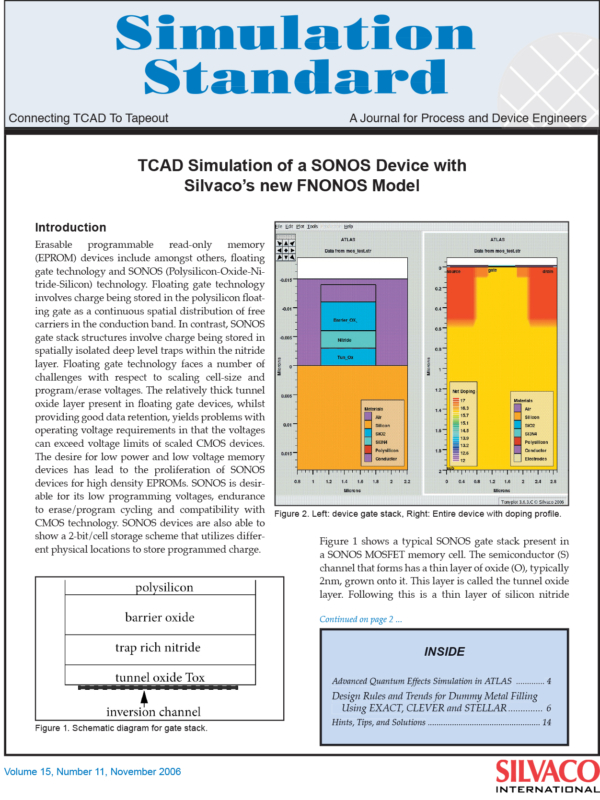
Figure 1 shows a typical SONOS gate stack present in a SONOS MOSFET memory cell. The semiconductor (S) channel that forms has a thin layer of oxide (O), typically 2nm, grown onto it. This layer is called the tunnel oxide layer. Following this is a thin layer of silicon nitride (N), typically 4 to 5 nm thick. Following this is a thicker layer of oxide (O), typically 5 to 6nm thick. This layer is called the barrier or capping layer. Finally we have a semiconducting polysilicon (S) gate layer. The nitride layer is made up of trap rich nitride so that is has trapping levels located within it. The nitride-oxide band offset allows charge to be accumulated in the nitride layer.


