SPICE Model Generation by Machine Learning
by Thomas Blaesi
It was 1988 when I got into SPICE (Simulation Program with Integrated Circuit Emphasis) while I was characterizing a 1.5 μm Standard cell library developed by students at my Alma-Mata Furtwangen University in Germany. My professor Dr. Nielinger was not only my advisor he also wrote the first SPICE bible in German language. At that time SPICE simulation was already established as the “golden” Simulator for circuit design for over a decade&and remains so to this day.
Of course, SPICE simulators went through several evolutions to adapt to the requirements of the most advanced technologies nodes, and SPICE models have been extended to be able to accurately reflect real silicon behavior; however, it seems that we are now at the point where it takes just too long to extend the models or come up with a complete new model for a specific material.
While over the first three decades only about half a dozen materials where used to manufacture semiconductors, ASM a leading semiconductor equipment manufacturer predicts that by 2020 more than 40 different materials will be in high volume production for the most advanced FinFET nodes at 7 and 5 nm.
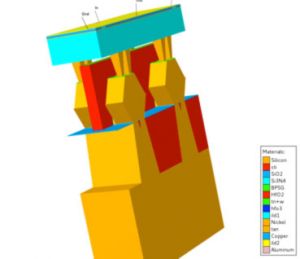
 Figure shows a 3D representation of a 10nm FinFET transistor front-end-of-line (FEOL) and back end of line up to MET1 already requires 14 different materials. A similar number of materials are required for full back end of line (BEOL) description.
With today’s display technologies especially, organic materials create a headache for accurately modeling their behavior with existing SPICE models. This is exacerbated by the fact that SPICE simulators and models are available from multiple vendors, requiring major collaboration between semiconductor companies, research institutions and tool suppliers. They are often led by the research institutions in order to develop and standardize new SPICE models, leaving the semiconductor companies with no choice but to run extremely expensive test wafers through their fabs and spend months developing and characterizing their foundation IP, creating terabytes of data and diverting highly valued engineers to repetitive menial jobs.
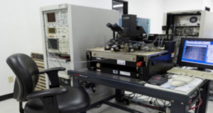
 I’m now at Silvaco, a Silicon Valley company around for over 34 years. We are in the business of transistor level design and SPICE simulation for a long time. We have a lab where we put devices under test and extract electrical parameters. We then feed the data into a tool called Utmost IV, which does the curve fitting and spice model generation. We also have TCAD device level modeling tools which allow you to model many of those 40 materials used in today’s semiconductor processes. In Victory 3D, Silvaco’s most advanced TCAD product, designers have access to a 3D process simulation tool and a device field solver that creates IV curves. Those are then fed into Utmost, which does its magic and generates the SPICE models. This approach is very effective and is provided at Silvaco today as a service to many customers around the world. We also sell the TCAD, SmartSpice and Utmost tools to major semiconductor companies.
New materials
With our TCAD tools we are also engaged with customers who do process development and therefore are deeply involved in simulation of new materials such as GaN and new technologies such as Nanotubes and OLED. We can foresee that the above described approach is breaking down since it needs a large amount of measured data and numerous iterations to create an accurate curve fitting.
In 2015 Silvaco acquired Infiniscale a startup in Grenoble, France. Their scientist and software developers have spent years applying machine learning algorithms to solve the most time consuming, most data generating circuit characterization issues. The first commercially available product that came out of that group was VarMan, a machine learning, Monte-Carlo based variation analysis tool to achieve high Sigma. TechModeler is the name of the tool that uses advanced neural networks that have the ability to learn relationships based on prior training. A patented incremental input sampling algorithm is feeding a unique neural networks methodology that dynamically creates multi-layered networks.
Using machine learning to create behavioral Verilog-A models
Using the self-learning capabilities of neural networks (NN) has been investigated and researched by academia for quite some time. The universality theorem is that neural networks with a single hidden layer can be used to approximate any continuous function to any desired precision. The guarantee is that by using enough hidden neurons we can always find a neural network whose output g(x) satisfies |g(x)−f(x)|<ϵ, for all inputs x. In other words, the output from the neural net will be correct to within the desired level of accuracy for every possible input value.
The biggest advantage of TechModeler’s approach is that a fairly small number of samples results in very reasonable accuracy, thus speeding up the availability of highly accurate models. The tool flow is highly automated and eliminates those long curve-fitting incremental approaches. TechModeler can also handle a huge number of variables and highly nonlinear phenomena to model effects such as temperature effects and self-heating, corner modeling for device variations, device and circuit reliability simulations and noise modeling.
Modeling of new technologies and phenomena
To illustrate TechModeler’s capabilities, here is an example of modeling the effect of Negative Bias Illumination Stress on an Indium gallium zinc oxide (IGZO), which is a semiconducting material, consisting of indium (In), gallium (Ga), zinc (Zn) and oxygen (O). IGZO thin-film transistor (TFT) is mostly used in the backplane of flat-panel displays (FPDs). Alternative solutions are attempting a curve fitting approach to conventional MOSFET or TFT SPICE models. None of them give you the accuracy and parametrization capabilities the behavioral Verilog-A model created by TechModeler is providing.

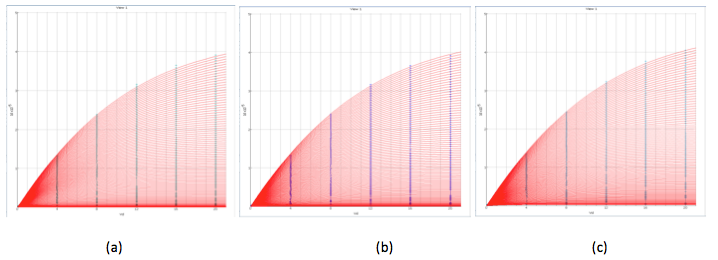
Figure: Id-Vd characteristics of the IGZO device under Negative Bias Illumination Stress for 0 (a), 100 hours (b) and 200 hours (c) of stress time, respectively. The dots represent the data and the red lines represent the model generated using TechModeler.

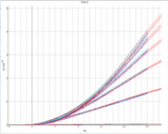
Figure: Combined Id-Vg characteristics of the IGZO device under Negative Bias Illumination Stress. The dots represent the data and the red lines represent the model generated using TechModeler.
Summary
In 1988 I couldn’t imagine that SPICE would still be the “golden” simulator 30 years later. All the other tools I have used then are long gone. Over the years I was involved in many new developments in EDA, on the Semiconductor side and EDA vendor side, in large corporations and in startups. I spent time driving the development of new place and route tools, logic verification and even system level design tools. Here at Silvaco I feel like I’m back where I started, and the most amazing thing is that there is still plenty of innovation to be researched and developed on the transistor level. I discovered the importance and power of material simulation in our TCAD tool Victory 3D, the capability of extracting the electrical parameters and translating them with TechModeler in a circuit simulation with SmartSpice. Who said you can’t teach an old dog a new trick?

