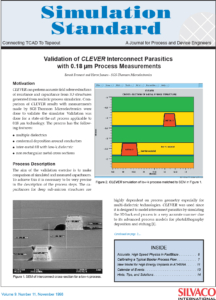
Validation of CLEVER Interconnect Parasitics with 0.18 µm Process Measurements Benoit Froment and Herve Jaouen-SGS-Thomson Microelectronics
Motivation
CLEVER can perform accurate field solver extractions of resistance and capacitance from 3D structures generated from realistic process simulation. Comparison of CLEVER results with measurements made by SGS-Thomson Microelectronics were done to validate the simulator. Validation was done for a state-of-the-art process applicable to 0.18 µm technology. The process has the following features:
- multiple dielectrics
- conformal deposition around conductors
- inter-metal fill with low-k dielectric
- non rectangular metal cross sections
Process Description
The aim of the validation exercise is to make comparison of simulated and measured capacitances. To achieve this it is necessary to be very precise in the description of the process steps. The capacitances for deep sub-micron structures are highly dependent on process geometry especially for multi-dielectric technologies. CLEVER was used since it is designed to model interconnect parasitics by simulating the 3D back end process in a very accurate manner due to its advanced process models for photolithography deposition and etching [1].
The measurements and CLEVER simulations were carried out with the ST HCMOS7X process. The pitch is 1um and the part of SiO2 usually deposited by plasma (ECR), is replaced by a low-k material gapfill (Fox). The Fox thickness target is around 600nm. The permittivity of Fox deposited between metal line is around 3, whereas the dielectric constant of the TEOS capping layer is 4.2. However, there is a slight variation on these values due to the process dispersion. It is assumed that these fluctuations are under 5% of the initial value.


