Using Luminous to Model the Transient Response of a Silicon Charge Collection and Transfer Structure
The rapid evolution of modern photonic devices in digital photographic and detection systems creates a need for physically-based simulation of charge collection and transfer. In this article we show the linearity, spatial sensitivity, and spectral response of a generalized silicon pixel structure using the Luminous module of the ATLAS device simulator. The Luminous module is used to simulate net charge generation due to incident light energy, and the S-Pisces module is used to simulate charge transport and generation-recombination mechanisms using the standard drift-diffusion transport equations coupled with Shockley-Read-Hall, Auger, and optical generation-recombination models.
Pixel Structure
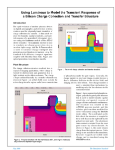
The charge collection structure modeled here is typical of imaging applications, where charge is formed by electron-hole pair generation due to light incident on the silicon substrate. The charge is kept confined laterally by a transfer channel stop, shown in Figure 1 as a thick field oxide outside the active charge transfer region, and a lower concentration of phosphorus under the gate region. Generally, the charge transfer in pixel and charge-coupled devices is due to diffusion, drift due to the electric field, and fringing electric field effects. Free charge-transfer is used to simulate these mechanisms by modeling only the free electrons in the conduction band.


