Enabling the Next Generation of High-Voltage Power: Ga2O3 Trench Schottky Diodes from Simulation to System
 β-Ga2O3 is set to revolutionize high-voltage power conversion, with ultra-low losses and a high critical electric field that make it ideal for next-generation power devices [1], enabling three-phase HVDC AC/DC and DC/AC conversion in the 1–6 kV, 0.5–0.8 kA range for AI data centre power delivery, renewable energy systems [2], high-voltage circuit breakers, and ESD protection [3].
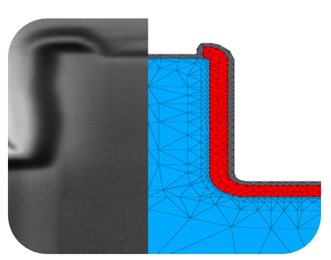
Achieving p-type β-Ga2O3 is challenging due to inherent material properties inhibiting practical hole conductivity [4], thus limiting the formation of p-n junctions which are widely utilized in power and logic devices for current rectification. In the absence of p–n homojunctions, β-Ga2O3 diodes initially must rely on Schottky junction architectures [5]. In recent years, lateral β-Ga2O3 SBDs with field-plate structures have demonstrated impressive breakdown voltages (BV) (>10 kV) [8]. However, vertical device architectures are preferred for their inherent ability to scale to higher currents and voltages by adjusting the epitaxial layer thickness while conserving die area [9]. Furthermore, reduced surface field (RESURF) techniques are applied to β-Ga2O3-based Schottky barrier diodes (SBDs) in order to mitigate high electric fields at the Schottky contact, and thus suppress reverse leakage (JR) that can occur due to thermionic field emission [6], image-force barrier lowering [6], and trap-assisted tunnelling from plasma etching [7]. This has resulted in the β-Ga2O3 vertical trench Schottky barrier diode (TSBD) being preferred device architecture, in which fins used for Schottky contact formation are separated by trenches that enable the RESURF effect to be implemented through use of an Al2O3-enabled vertical metal-oxide-semiconductor (MOS) junction on the fin sidewall. The failure of TSBD is governed by dielectric breakdown rather than the metal–semiconductor junction. While Al2O3 can sustain fields up to ~8.7 MV/cm [10], electric field crowding at the trench corner leads to the critical electric field being exceeded in the dielectric layer in that region. Thus, under reverse bias, high fields in the dielectric can cause catastrophic failure, and thicker dielectrics – although more robust, may reduce RESURF effectiveness in the fins [9]. It is essential to develop simulation models at an early stage to study the effect of device geometries on the device handling capabilities and develop compact models for SPICE-based circuit simulations.
This simulation report showcases a β-Ga2O3 TSBD, progressing from experimentally derived TCAD modelling to compact model extraction and SPICE-level circuit analysis. The β-Ga2O3 TSBDs are fabricated and electrically tested at University of Bristol cleanroom and characterization lab facilities, process simulation is defined using Victory Process, Victory Mesh, Victory Device and the SPICE modelling were performed using Utmost4, Gateway and SmartSpice tools.


