TCAD Breakdown Simulation of a 1200 V Vertical GaN FinFET
Khaled Ahmeda, Nereus Agbo & Xiang Li
Research and Development Centre, Dynex Semiconductor Ltd, Doddington Rd, Lincoln LN6 3LF, United Kingdom
Abstract
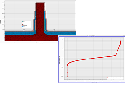 This paper presents TCAD process, mesh, and device simulations of a 1200 V vertical gallium nitride (GaN) FinFET using Silvaco Victory tools. The simulated structure is based on a previously reported vertical GaN FinFET fabricated on bulk GaN substrates, comprising an n+ GaN cap, a lightly doped drift region, and an Al2O3 gate dielectric. The process flow is reproduced in Victory Process, followed by mesh generation in Victory Mesh and electrical simulation in Victory Device using physical models that include Shockley–Read–Hall recombination, Auger recombination, band-to-band tunnelling, Schottky tunnelling, self-heating, and impact ionization. The simulation reproduces breakdown behaviour at approximately 1200 V, with low drain and gate leakage currents. Analysis of the electric field, impact generation rate, and current density indicates that breakdown is governed by electric-field crowding at the bottom of the fin. These results demonstrate the capability of TCAD simulation to capture the breakdown behavior of vertical GaN FinFETs and provide insight into the critical regions that determine high-voltage performance.

