Modeling and Parameter Extraction Technique for HV MOS Devices with BSIM3v3
1. Introduction
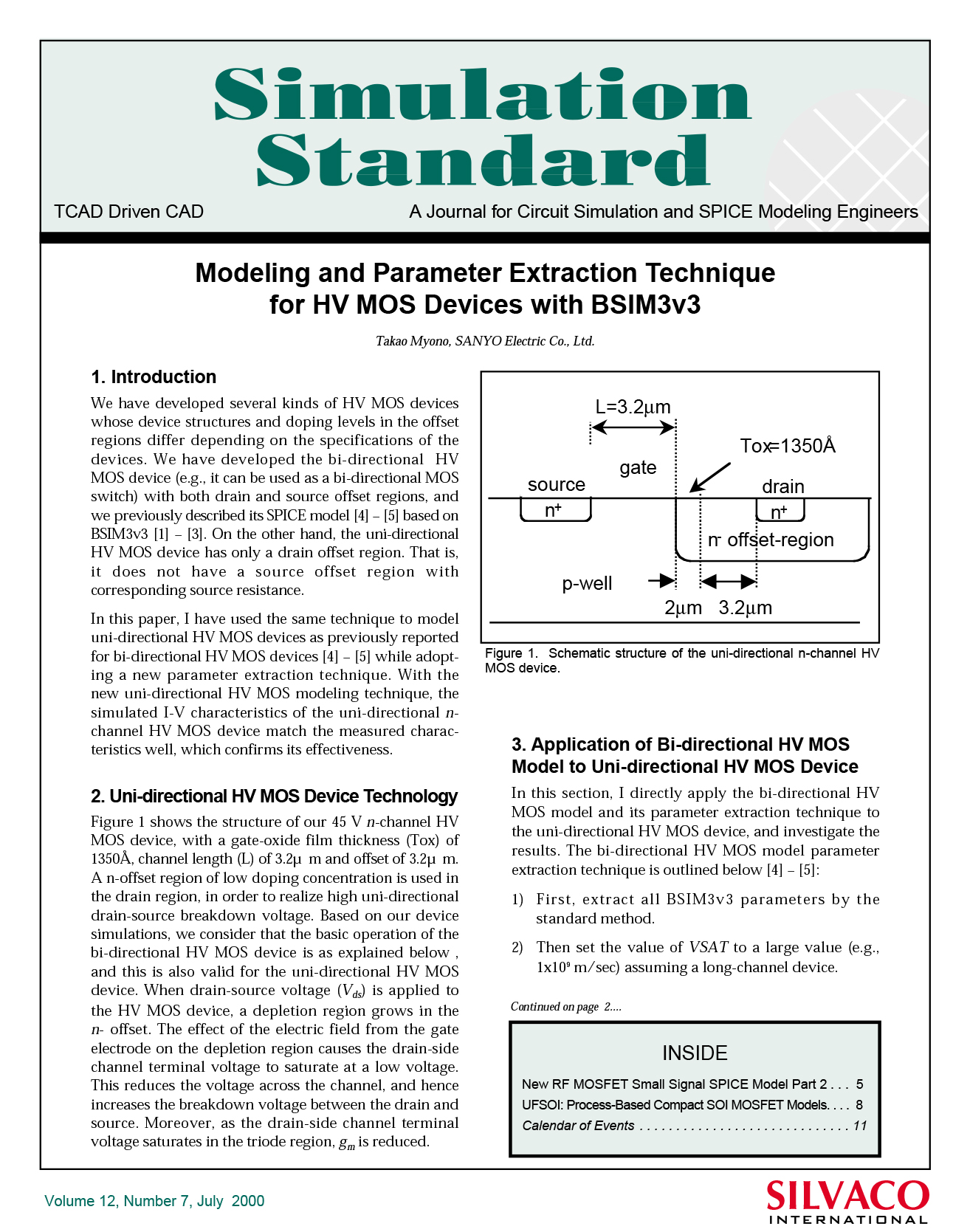
We have developed several kinds of HV MOS devices whose device structures and doping levels in the offset regions differ depending on the specifications of the devices. We have developed the bi-directional HV MOS device (e.g., it can be used as a bi-directional MOS switch) with both drain and source offset regions, and we previously described its SPICE model [4]&[5] based on BSIM3v3 [1]&[3]. On the other hand, the uni-directional HV MOS device has only a drain offset region. That is, it does not have a source offset region with corresponding source resistance.
In this paper, I have used the same technique to model uni-directional HV MOS devices as previously reported for bi-directional HV MOS devices [4] -[5] while adopting a new parameter extraction technique. With the new uni-directional HV MOS modeling technique, the simulated I-V characteristics of the uni-directional n-channel HV MOS device match the measured characteristics well, which confirms its effectiveness.


