Estimation of Interface Property Changes Between Normally On/Off Hydrogenated Diamond MISFETs
Introduction
Diamond is considered to be the ultimate semiconductor material for high power and high frequency devices due to its superior electrical and thermal properties, such as high breakdown field, high carrier mobility, low dielectric constant, and high thermal conductivity, as shown in Table 1.
Furthermore, diamond has some unique electronic properties. The surface of diamond films terminated by hydrogen atoms has negative electron affinity (NEA) and can generate a two-dimensional hole accumulation layer suitable as a hole channel of a field-effect transistor.
Although the mechanisms of NEA and hole accumulation phenomena have not been fully elucidated yet, thermal annealing can be used to control them to some extent in metal-insulator-semiconductor field-effect transistors (MISFETs).
The purpose of this article is to find and estimate one of the possibilities as to what kind of device properties have been changed by the annealing quantitatively using TCAD calibration with experimental I-V curves.
Device Structure and Simulation Models
The experimental data targeted were quoted from a paper which clearly showed the effect of the annealing on the normally on/off characteristics of the hydrogenated diamond (H-diamond) MISFETs [3].
According to the paper, the devices were fabricated as follows. H-diamond epitaxial layers were grown by microwave plasma-enhanced CVD on single-crystalline diamond (001) substrates.
For the normally off MISFET, the gate insulator and contact are fabricated first and annealed at 180℃, then source/drain ohmic contacts are fabricated. For the normally on MISFET, source/drain ohmic contacts are fabricated first, then gate insulator and contact are fabricated without annealing.
The gate insulator composed of a 4nm Al2O3 buffer layer on the H-diamond layer and 23.4nm LaAlO3 layer on the buffer layer were deposited.
The gate length is 4um and the interspacing between the source/drain ohmic contact and gate insulator is 5um.
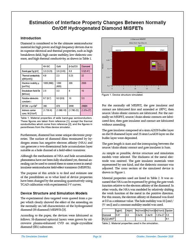
As simple as possible, device structure and simulation models were selected. The thickness of the metal electrode was omitted. The gate insulator materials were represented by one kind, and the dielectric constant was adjusted.


