Atlas Simulation of a Wide Bandgap Gallium Oxide (Ga2O3) MOSFET
Introduction
Single-crystal gallium oxide (Ga2O3) has attracted increasing attention as a promising material for power device applications. It possesses excellent material properties and has the potential for mass productivity of low-cost and high-quality bulk crystals by using methods such as the edge-defined film-fed growth (EFG) method [1].
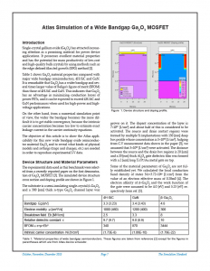
Table 1 shows Ga2O3 material properties compared with major wide bandgap semiconductors, 4H-SiC and GaN. It is remarkable that Ga2O3 has a wider bandgap and several times larger value of Baliga’s figure of merit (BFOM) than those of 4H-SiC and GaN. This indicates that Ga2O3 has an advantage in minimizing conduction losses of power FETs, and it can be expected to exceed 4H-SiC and GaN performances when used for high-power and high-voltage applications.


