
Simulation Standard
Silvaco面向半导体工艺和器件仿真工程师推出的技术刊物
 https://silvaco.com/wp-content/uploads/2020/03/simstd_Q1_2010_a2.jpg
1012
782
Ingrid Schwarz
/wp-content/uploads/2019/11/silvaco-logo.png
Ingrid Schwarz2010-01-01 14:46:062021-10-13 10:25:55Modeling and Optimization of CIGS Solar Cell Module
https://silvaco.com/wp-content/uploads/2020/03/simstd_Q1_2010_a2.jpg
1012
782
Ingrid Schwarz
/wp-content/uploads/2019/11/silvaco-logo.png
Ingrid Schwarz2010-01-01 14:46:062021-10-13 10:25:55Modeling and Optimization of CIGS Solar Cell Module https://silvaco.com/wp-content/uploads/2020/03/simstd_Q1_2010_a1.jpg
1012
782
Ingrid Schwarz
/wp-content/uploads/2019/11/silvaco-logo.png
Ingrid Schwarz2010-01-01 14:38:362021-10-13 10:25:55Using VICTORY PROCESS for Rapid Geometry Prototyping
https://silvaco.com/wp-content/uploads/2020/03/simstd_Q1_2010_a1.jpg
1012
782
Ingrid Schwarz
/wp-content/uploads/2019/11/silvaco-logo.png
Ingrid Schwarz2010-01-01 14:38:362021-10-13 10:25:55Using VICTORY PROCESS for Rapid Geometry Prototyping https://silvaco.com/wp-content/uploads/2020/03/simstd_Q4_2009_a3.jpg
1012
782
Ingrid Schwarz
/wp-content/uploads/2019/11/silvaco-logo.png
Ingrid Schwarz2009-10-01 16:53:222021-10-13 10:25:553D SOI NMOSFET Simulation Using VICTORY DEVICE
https://silvaco.com/wp-content/uploads/2020/03/simstd_Q4_2009_a3.jpg
1012
782
Ingrid Schwarz
/wp-content/uploads/2019/11/silvaco-logo.png
Ingrid Schwarz2009-10-01 16:53:222021-10-13 10:25:553D SOI NMOSFET Simulation Using VICTORY DEVICE https://silvaco.com/wp-content/uploads/2020/03/simstd_Q4_2009_a2.jpg
1012
782
Ingrid Schwarz
/wp-content/uploads/2019/11/silvaco-logo.png
Ingrid Schwarz2009-10-01 16:50:472021-10-13 10:25:56Crosstalk Simulation in InSb Detector Arrays
https://silvaco.com/wp-content/uploads/2020/03/simstd_Q4_2009_a2.jpg
1012
782
Ingrid Schwarz
/wp-content/uploads/2019/11/silvaco-logo.png
Ingrid Schwarz2009-10-01 16:50:472021-10-13 10:25:56Crosstalk Simulation in InSb Detector Arrays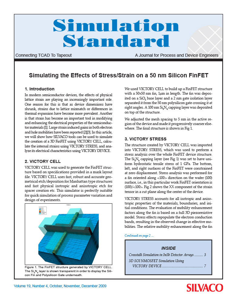 https://silvaco.com/wp-content/uploads/2020/03/simstd_Q4_2009_a1.jpg
1012
782
Ingrid Schwarz
/wp-content/uploads/2019/11/silvaco-logo.png
Ingrid Schwarz2009-10-01 16:48:332021-10-13 10:29:43Simulating the Effects of Stress/Strain on a 50 nm Silicon FinFET
https://silvaco.com/wp-content/uploads/2020/03/simstd_Q4_2009_a1.jpg
1012
782
Ingrid Schwarz
/wp-content/uploads/2019/11/silvaco-logo.png
Ingrid Schwarz2009-10-01 16:48:332021-10-13 10:29:43Simulating the Effects of Stress/Strain on a 50 nm Silicon FinFET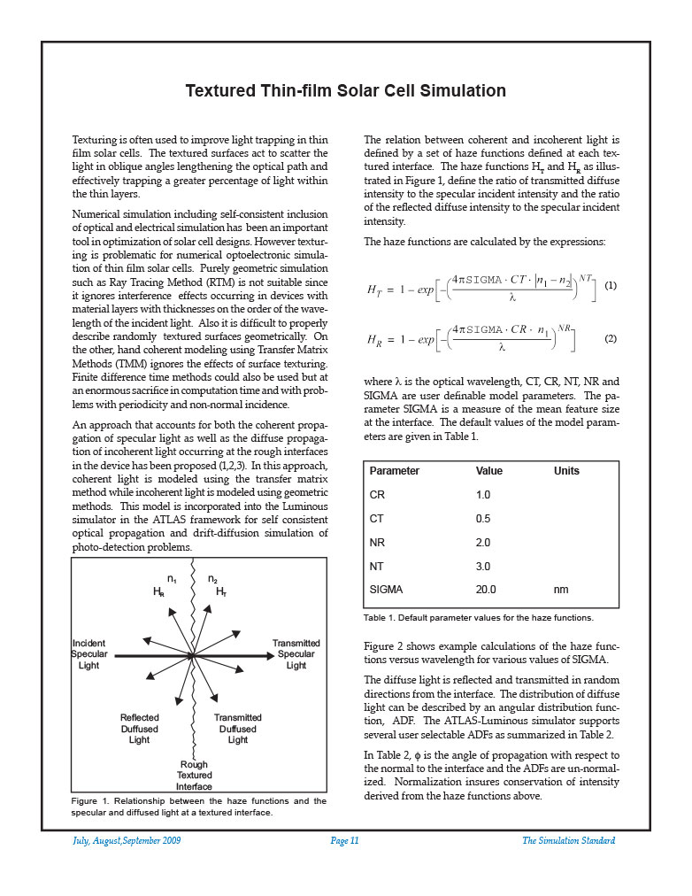 https://silvaco.com/wp-content/uploads/2020/03/simstd_Q3_2009_a4.jpg
1012
782
Ingrid Schwarz
/wp-content/uploads/2019/11/silvaco-logo.png
Ingrid Schwarz2009-07-01 16:46:242021-10-13 10:29:43Textured Thin-film Solar Cell Simulation
https://silvaco.com/wp-content/uploads/2020/03/simstd_Q3_2009_a4.jpg
1012
782
Ingrid Schwarz
/wp-content/uploads/2019/11/silvaco-logo.png
Ingrid Schwarz2009-07-01 16:46:242021-10-13 10:29:43Textured Thin-film Solar Cell Simulation