Simulation Standard
Silvaco面向半导体工艺和器件仿真工程师推出的技术刊物
SONOS/SANOS Simulation in ATLAS
Semiconductor-Oxide-Nitride-Oxide-Semiconductor (SONOS) Non-Volatile memory structures can be simulated using ATLAS. The basic principle of these devices is the use of a charge trapping Silicon Nitride layer embedded in the oxide layer separating the gate from the channel. This results in an oxide layer between the gate and the Silicon Nitride layer, and another between the Nitride layer and the semiconducting channel (Figure 1). The Silicon Nitride layer can be charged by quantum mechanical tunneling or by hot carrier injection. This results in a shift in the turn-on voltage of the NVM device. The trapped charge can be discharged by quantum mechanical tunneling or by injecting hot carriers of the opposite polarity, thereby erasing the threshold Voltage shift.[1] [2]
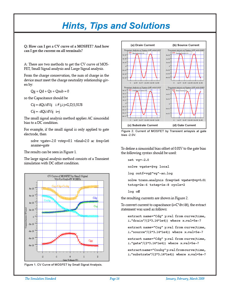
Hints, Tips and Solutions – Determining the CV Curve and Terminal Currents of a MOSFET
Q: How can I get a CV curve of a MOSFET? And how can I get the current on all terminals?
A: There are two methods to get the CV curve of MOSFET, Small Signal analysis and Large Signal analysis.
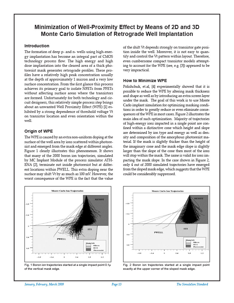
Minimization of Well-Proximity Effect by Means of 2D and 3D Monte Carlo Simulation of Retrograde Well Implantation
The formation of deep p- and n- wells using high-energy implantation has become an integral part of CMOS technology process flow. The high energy and high dose implantation into the cleared area of a thick photoresist mask generates retrograde profiles. These profiles have a relatively high peak concentration usually at the depth of approximately 1 micron and a very low surface concentration. From the first glance this process achieves its primary goal to isolate NFETs from PFETs without affecting surface areas where the transistors are formed. Unfortunately for both technology and circuit designers, this relatively simple process step brings about an unwanted Well Proximity Effect (WPE) [1] exhibited by a strong dependence of threshold voltage Vt on transistor location and even orientation within the well.
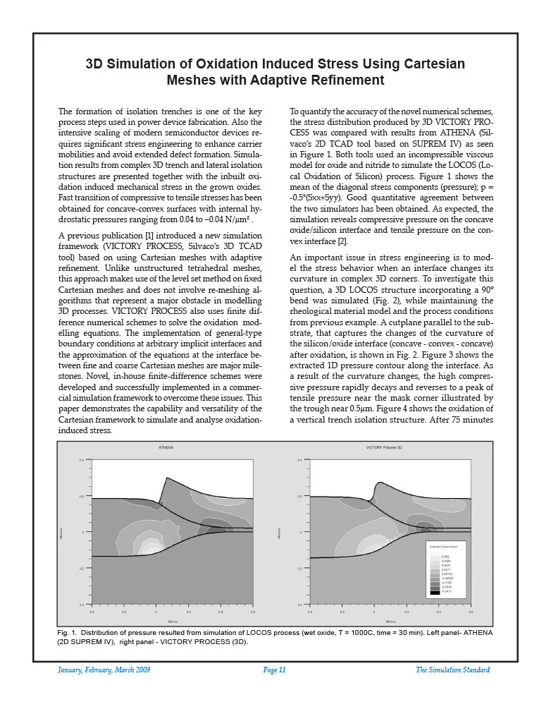
3D Simulation of Oxidation Induced Stress Using Cartesian Meshes with Adaptive Refinement
The formation of isolation trenches is one of the key process steps used in power device fabrication. Also the intensive scaling of modern semiconductor devices requires significant stress engineering to enhance carrier mobilities and avoid extended defect formation. Simulation results from complex 3D trench and lateral isolation structures are presented together with the inbuilt oxidation induced mechanical stress in the grown oxides. Fast transition of compressive to tensile stresses has been obtained for concave-convex surfaces with internal hydrostatic pressures ranging from 0.04 to –0.04 N/μm2 .
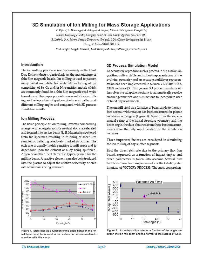
3D Simulation of Ion Milling for Mass Storage Applications
The ion milling process is used extensively in the Hard Disc Drive industry, particularly in the manufacture of thin film magnetic heads. Ion milling is used to pattern many metal and dielectric materials including alloys comprising of Fe, Co and/or Ni transition metals which are commonly found in a thin film magnetic read-write transducers. This paper presents new results for ion milling and redeposition of gold on photoresist patterns at different milling angles and compared with 3D process simulation results.
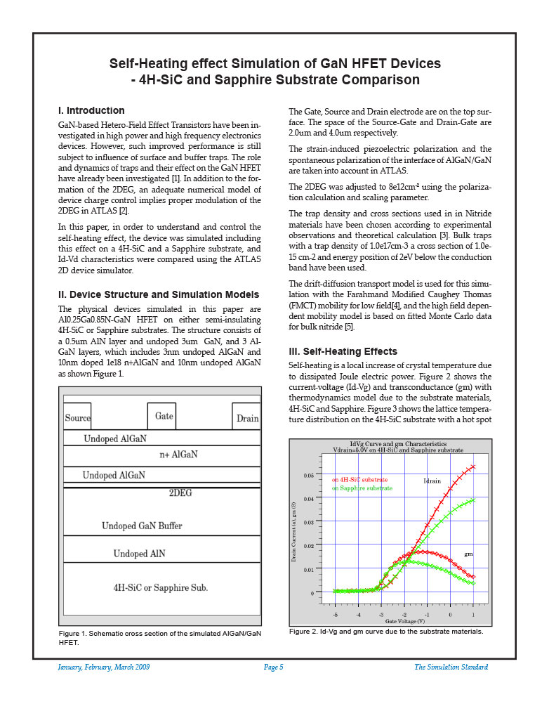
Self-Heating effect Simulation of GaN HFET Devices – 4H-SiC and Sapphire Substrate Comparison
GaN-based Hetero-Field Effect Transistors have been investigated in high power and high frequency electronics devices. However, such improved performance is still subject to influence of surface and buffer traps. The role and dynamics of traps and their effect on the GaN HFET have already been investigated [1]. In addition to the formation of the 2DEG, an adequate numerical model of device charge control implies proper modulation of the 2DEG in ATLAS [2].

