
Simulation Standard
Silvaco面向半导体工艺和器件仿真工程师推出的技术刊物
 https://silvaco.com/wp-content/uploads/simulationstandard/simstd_may_2007_a2-e1611193444254.jpg
800
644
Erick Castellon
/wp-content/uploads/2019/11/silvaco-logo.png
Erick Castellon2007-05-01 00:02:262021-10-13 10:30:51Electrical Stress Degradation of Small-Grain Polysilicon Thin-Film Transistors
https://silvaco.com/wp-content/uploads/simulationstandard/simstd_may_2007_a2-e1611193444254.jpg
800
644
Erick Castellon
/wp-content/uploads/2019/11/silvaco-logo.png
Erick Castellon2007-05-01 00:02:072021-10-13 10:30:51Trapping Effects in the Transient Response of AlGaN/GaN HEMT Devices
https://silvaco.com/wp-content/uploads/simulationstandard/simstd_may_2007_a2-e1611193444254.jpg
800
644
Erick Castellon
/wp-content/uploads/2019/11/silvaco-logo.png
Erick Castellon2007-05-01 00:02:262021-10-13 10:30:51Electrical Stress Degradation of Small-Grain Polysilicon Thin-Film Transistors
https://silvaco.com/wp-content/uploads/simulationstandard/simstd_may_2007_a2-e1611193444254.jpg
800
644
Erick Castellon
/wp-content/uploads/2019/11/silvaco-logo.png
Erick Castellon2007-05-01 00:02:072021-10-13 10:30:51Trapping Effects in the Transient Response of AlGaN/GaN HEMT Devices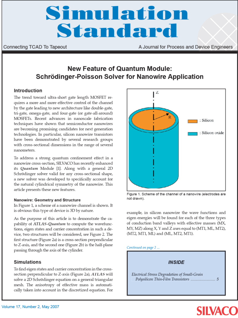 https://silvaco.com/wp-content/uploads/simulationstandard/simstd_may_2007_a1.jpg
1669
1252
Erick Castellon
/wp-content/uploads/2019/11/silvaco-logo.png
Erick Castellon2007-05-01 00:01:242021-10-13 10:30:51New Feature of Quantum Module: Schrödinger-Poisson Solver for Nanowire Application
https://silvaco.com/wp-content/uploads/simulationstandard/simstd_may_2007_a1.jpg
1669
1252
Erick Castellon
/wp-content/uploads/2019/11/silvaco-logo.png
Erick Castellon2007-05-01 00:01:242021-10-13 10:30:51New Feature of Quantum Module: Schrödinger-Poisson Solver for Nanowire Application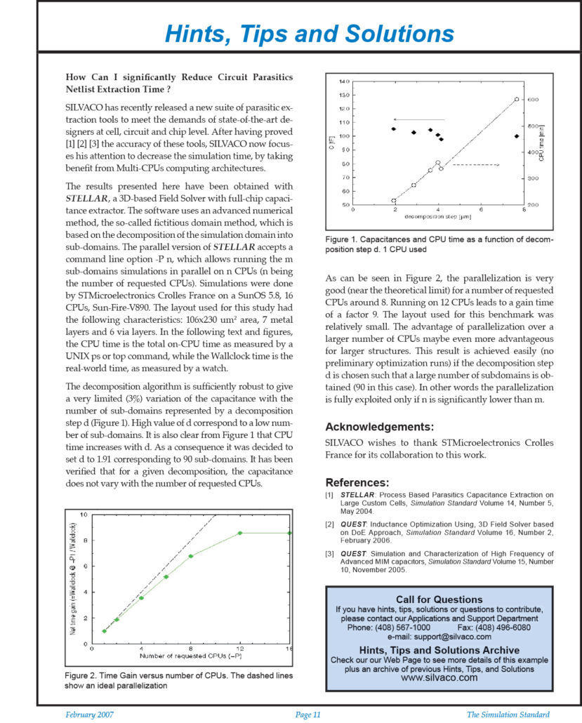 https://silvaco.com/wp-content/uploads/simulationstandard/simstd_feb_2007_hints-e1611194185247.jpg
800
644
Erick Castellon
/wp-content/uploads/2019/11/silvaco-logo.png
Erick Castellon2007-02-01 00:04:442021-10-13 10:30:51How Can I significantly Reduce Circuit Parasitics Netlist Extraction Time?
https://silvaco.com/wp-content/uploads/simulationstandard/simstd_feb_2007_hints-e1611194185247.jpg
800
644
Erick Castellon
/wp-content/uploads/2019/11/silvaco-logo.png
Erick Castellon2007-02-01 00:04:442021-10-13 10:30:51How Can I significantly Reduce Circuit Parasitics Netlist Extraction Time?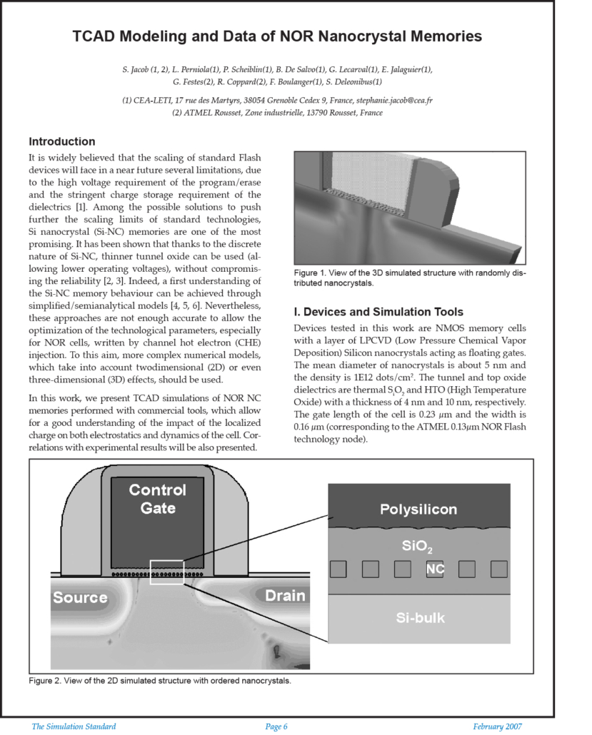 https://silvaco.com/wp-content/uploads/simulationstandard/simstd_feb_2007_a2.jpg
1669
1344
Erick Castellon
/wp-content/uploads/2019/11/silvaco-logo.png
Erick Castellon2007-02-01 00:02:292021-10-13 10:30:59TCAD Modeling and Data of NOR Nanocrystal Memories
https://silvaco.com/wp-content/uploads/simulationstandard/simstd_feb_2007_a2.jpg
1669
1344
Erick Castellon
/wp-content/uploads/2019/11/silvaco-logo.png
Erick Castellon2007-02-01 00:02:292021-10-13 10:30:59TCAD Modeling and Data of NOR Nanocrystal Memories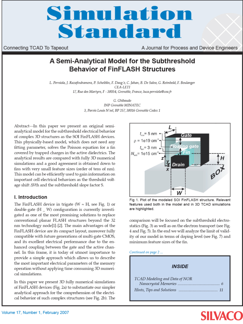 https://silvaco.com/wp-content/uploads/simulationstandard/simstd_feb_2007_a1.jpg
1669
1252
Erick Castellon
/wp-content/uploads/2019/11/silvaco-logo.png
Erick Castellon2007-02-01 00:01:282021-10-13 10:31:00A Semi-Analytical Model for the Subthreshold Behavior of FinFLASH Structures
https://silvaco.com/wp-content/uploads/simulationstandard/simstd_feb_2007_a1.jpg
1669
1252
Erick Castellon
/wp-content/uploads/2019/11/silvaco-logo.png
Erick Castellon2007-02-01 00:01:282021-10-13 10:31:00A Semi-Analytical Model for the Subthreshold Behavior of FinFLASH Structures