
Simulation Standard
Silvaco面向半导体工艺和器件仿真工程师推出的技术刊物
 https://silvaco.com/wp-content/uploads/simulationstandard/simstd_nov_2006_hints-e1611194324583.jpg
800
644
Erick Castellon
/wp-content/uploads/2019/11/silvaco-logo.png
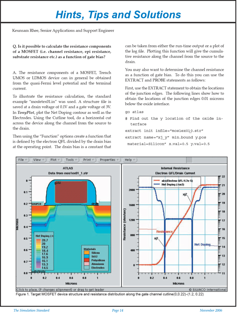
Erick Castellon2006-11-01 00:04:582021-10-13 10:31:00Is it possible to calculate the resistance components of a MOSFET
https://silvaco.com/wp-content/uploads/simulationstandard/simstd_nov_2006_hints-e1611194324583.jpg
800
644
Erick Castellon
/wp-content/uploads/2019/11/silvaco-logo.png
Erick Castellon2006-11-01 00:04:582021-10-13 10:31:00Is it possible to calculate the resistance components of a MOSFET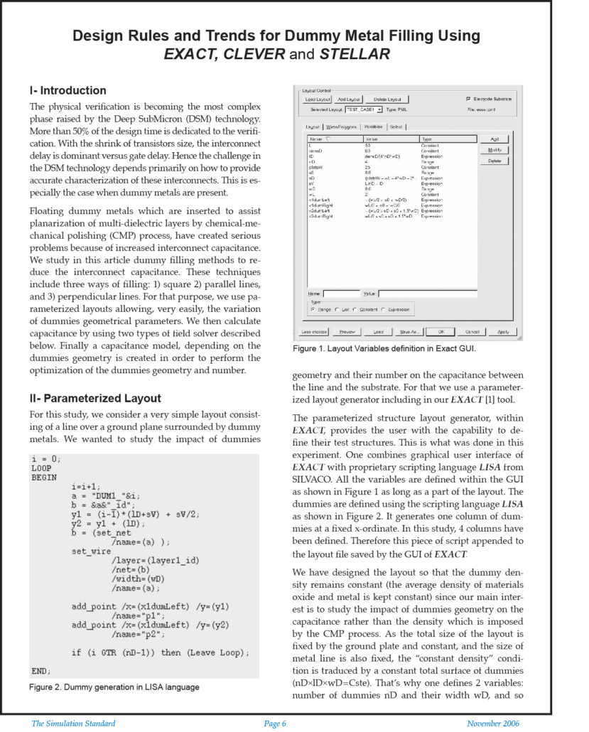 https://silvaco.com/wp-content/uploads/simulationstandard/simstd_nov_2006_a3.jpg
1669
1344
Erick Castellon
/wp-content/uploads/2019/11/silvaco-logo.png
Erick Castellon2006-11-01 00:03:472021-10-13 10:31:00Design Rules and Trends for Dummy Metal Filling Using Exact, Clever and Stellar
https://silvaco.com/wp-content/uploads/simulationstandard/simstd_nov_2006_a3.jpg
1669
1344
Erick Castellon
/wp-content/uploads/2019/11/silvaco-logo.png
Erick Castellon2006-11-01 00:03:472021-10-13 10:31:00Design Rules and Trends for Dummy Metal Filling Using Exact, Clever and Stellar https://silvaco.com/wp-content/uploads/simulationstandard/simstd_nov_2006_a2.jpg
1669
1344
Erick Castellon
/wp-content/uploads/2019/11/silvaco-logo.png
Erick Castellon2006-11-01 00:02:032021-10-13 10:31:00Advanced Quantum Effects Simulation in Atlas
https://silvaco.com/wp-content/uploads/simulationstandard/simstd_nov_2006_a2.jpg
1669
1344
Erick Castellon
/wp-content/uploads/2019/11/silvaco-logo.png
Erick Castellon2006-11-01 00:02:032021-10-13 10:31:00Advanced Quantum Effects Simulation in Atlas https://silvaco.com/wp-content/uploads/simulationstandard/simstd_nov_2006_a1-e1611193644926.jpg
800
600
Erick Castellon
/wp-content/uploads/2019/11/silvaco-logo.png
Erick Castellon2006-11-01 00:01:212021-10-13 10:31:08TCAD Simulation of a SONOS Device with Silvaco’s new FNONOS Model
https://silvaco.com/wp-content/uploads/simulationstandard/simstd_nov_2006_a1-e1611193644926.jpg
800
600
Erick Castellon
/wp-content/uploads/2019/11/silvaco-logo.png
Erick Castellon2006-11-01 00:01:212021-10-13 10:31:08TCAD Simulation of a SONOS Device with Silvaco’s new FNONOS Model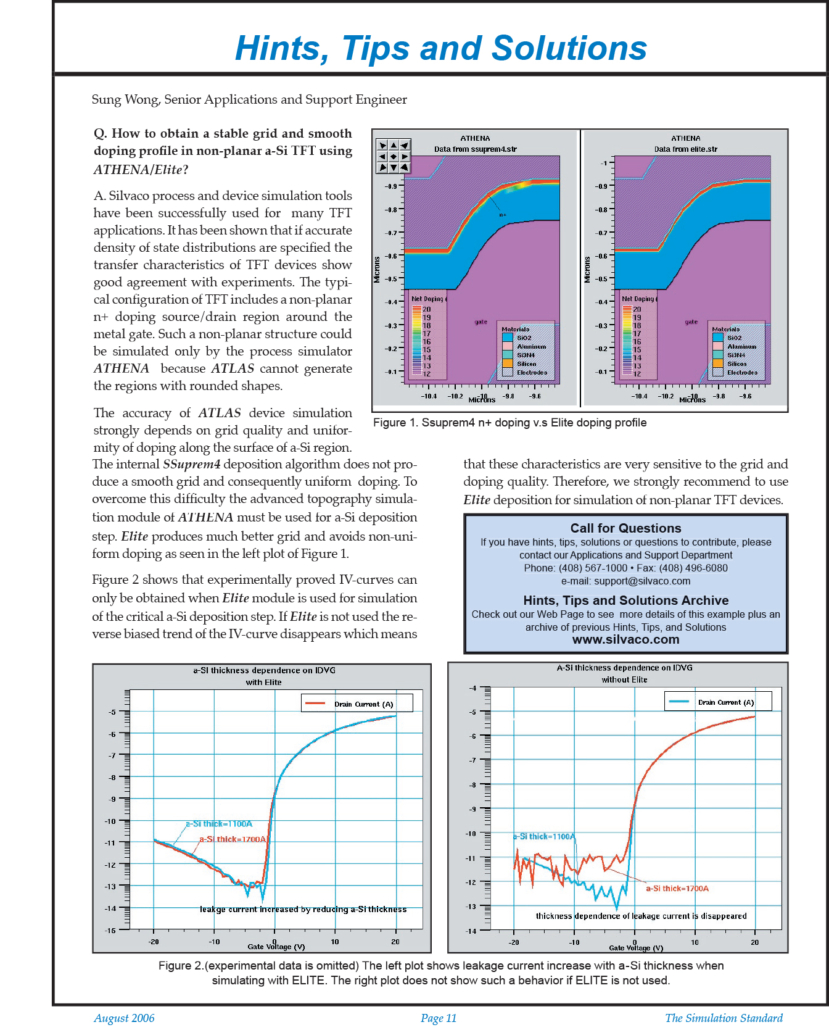 https://silvaco.com/wp-content/uploads/simulationstandard/simstd_aug_2006_hints-e1611193214797.jpg
800
644
Erick Castellon
/wp-content/uploads/2019/11/silvaco-logo.png
Erick Castellon2006-08-01 00:05:382021-10-13 10:31:08How to obtain a stable grid and smooth doping profile in non-planar a-Si TFT using Athena/Elite?
https://silvaco.com/wp-content/uploads/simulationstandard/simstd_aug_2006_hints-e1611193214797.jpg
800
644
Erick Castellon
/wp-content/uploads/2019/11/silvaco-logo.png
Erick Castellon2006-08-01 00:05:382021-10-13 10:31:08How to obtain a stable grid and smooth doping profile in non-planar a-Si TFT using Athena/Elite?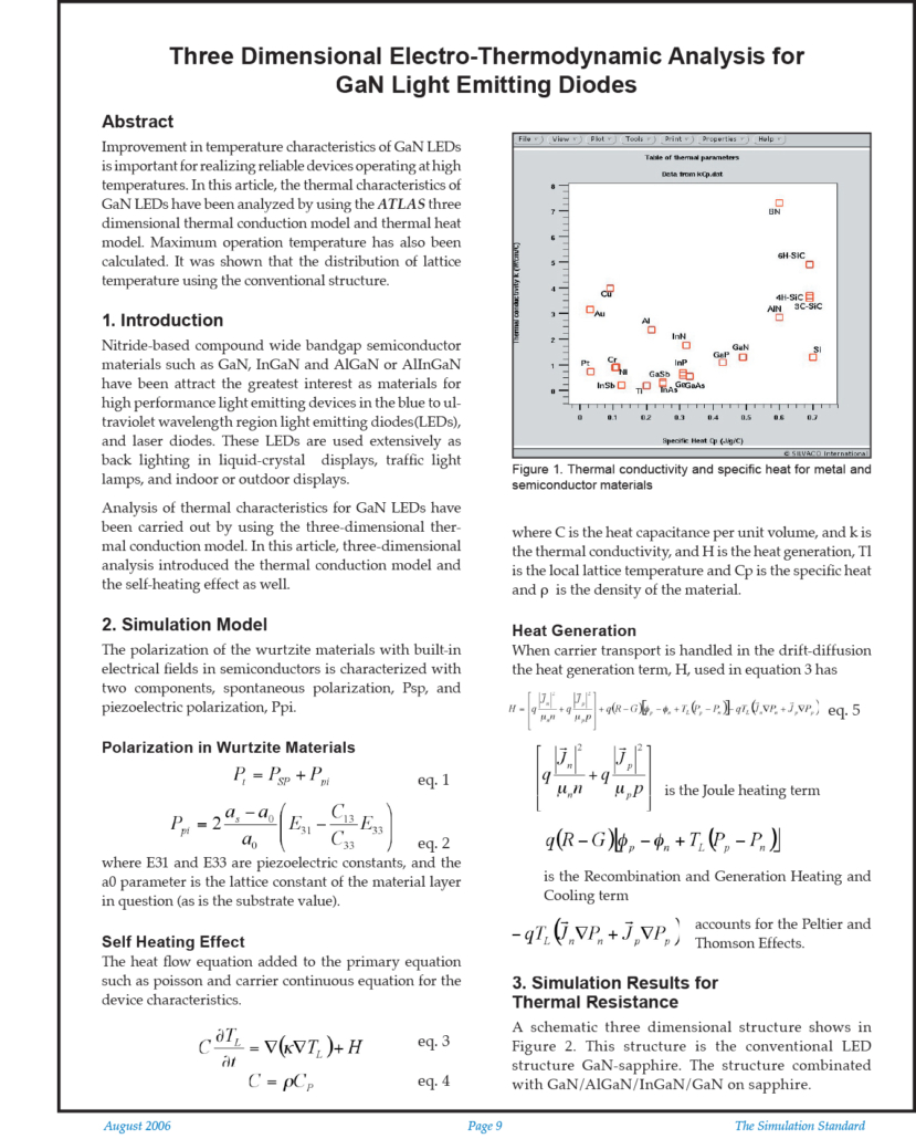 https://silvaco.com/wp-content/uploads/simulationstandard/simstd_aug_2006_a4.jpg
1669
1344
Erick Castellon
/wp-content/uploads/2019/11/silvaco-logo.png
Erick Castellon2006-08-01 00:04:292021-10-13 10:31:09Three Dimensional Electro-Thermodynamic Analysis for GaN Light Emitting Diodes
https://silvaco.com/wp-content/uploads/simulationstandard/simstd_aug_2006_a4.jpg
1669
1344
Erick Castellon
/wp-content/uploads/2019/11/silvaco-logo.png
Erick Castellon2006-08-01 00:04:292021-10-13 10:31:09Three Dimensional Electro-Thermodynamic Analysis for GaN Light Emitting Diodes