Simulation Standard
Silvaco面向半导体工艺和器件仿真工程师推出的技术刊物
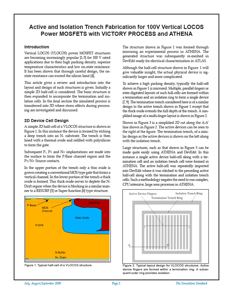
Active and Isolation Trench Fabrication for 100V Vertical LOCOS Power MOSFETS with VICTORY PROCESS and ATHENA
Vertical LOCOS (VLOCOS) power MOSFET structures are becoming increasingly popular [1-3] for 100 V rated applications due to their high packing density, superior temperature characteristics and low on-state resistance. It has been shown that through careful design, the on-state resistance can exceed the silicon limit [4].
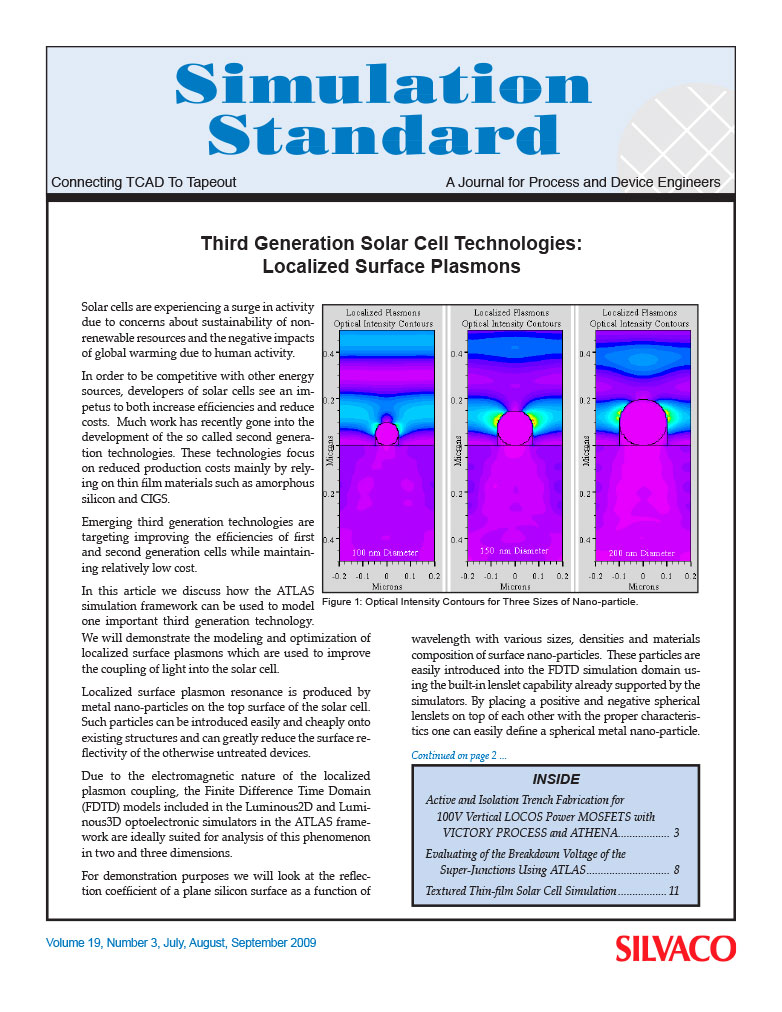
Third Generation Solar Cell Technologies: Localized Surface Plasmons
Solar cells are experiencing a surge in activity due to concerns about sustainability of non-renewable resources and the negative impacts of global warming due to human activity.
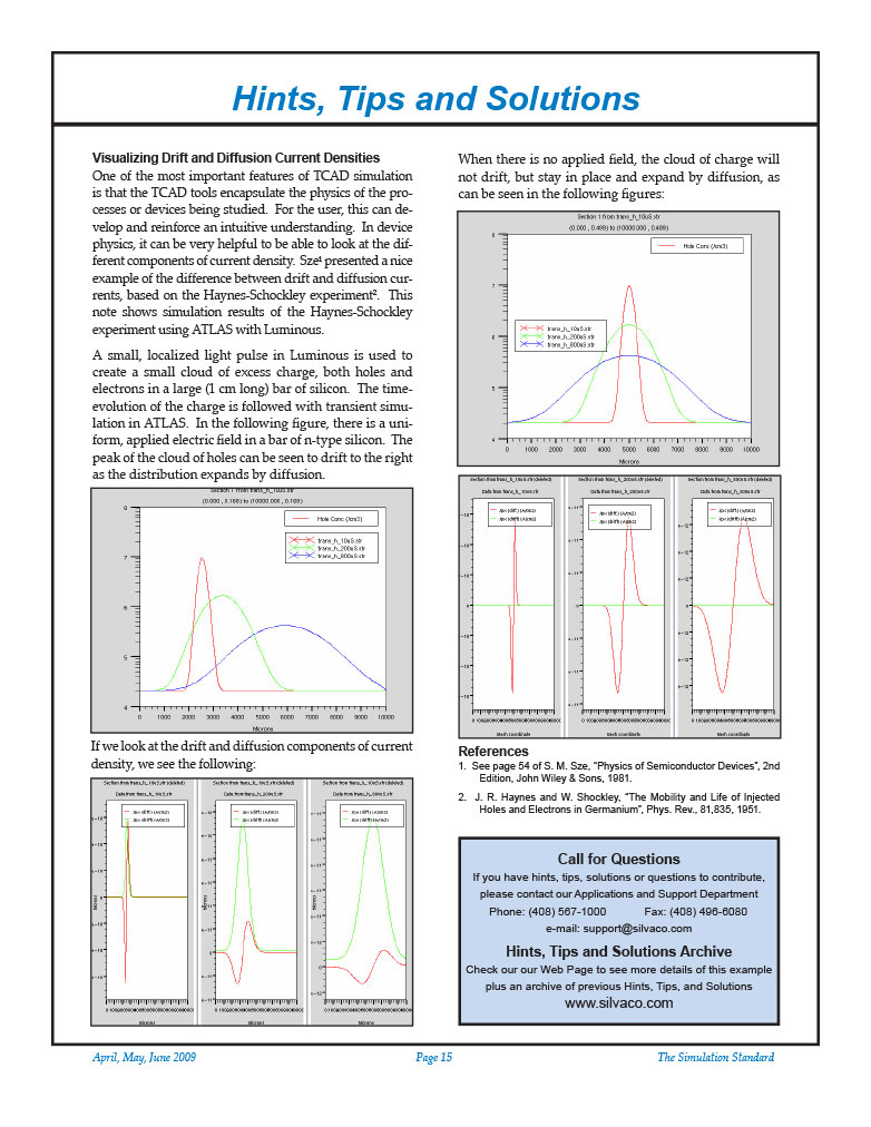
Hints, Tips and Solutions – Visualizing Drift and Diffusion Current Densities
One of the most important features of TCAD simulation is that the TCAD tools encapsulate the physics of the processes or devices being studied. For the user, this can develop and reinforce an intuitive understanding. In device physics, it can be very helpful to be able to look at the different components of current density. Sze1 presented a nice example of the difference between drift and diffusion currents, based on the Haynes-Schockley experiment2. This note shows simulation results of the Haynes-Schockley experiment using ATLAS with Luminous.
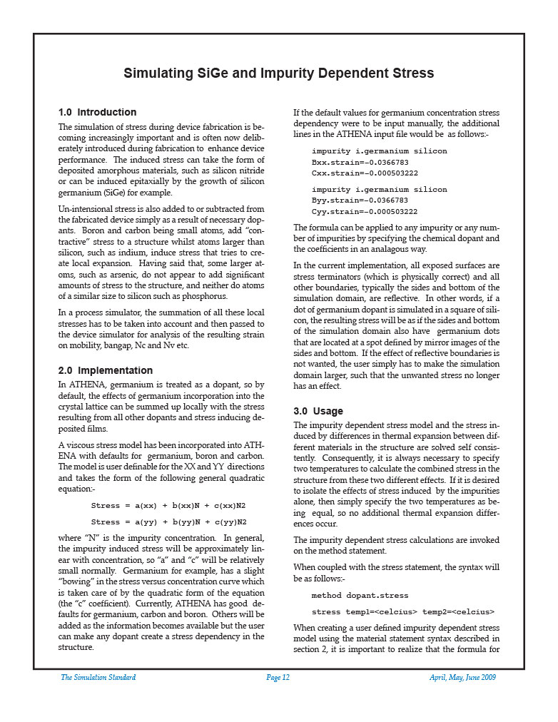
Simulating SiGe and Impurity Dependent Stress
The simulation of stress during device fabrication is becoming increasingly important and is often now deliberately introduced during fabrication to enhance device performance. The induced stress can take the form of deposited amorphous materials, such as silicon nitride or can be induced epitaxially by the growth of silicon germanium (SiGe) for example.
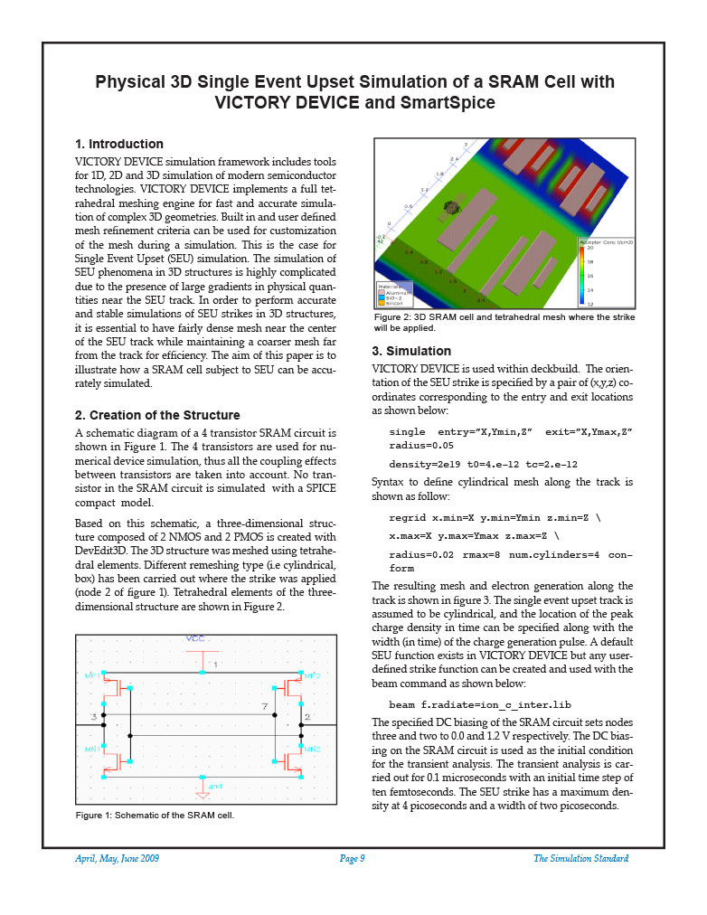
Physical 3D Single Event Upset Simulation of a SRAM Cell with VICTORY DEVICE and SmartSpice
VICTORY DEVICE simulation framework includes tools for 1D, 2D and 3D simulation of modern semiconductor technologies. VICTORY DEVICE implements a full tetrahedral meshing engine for fast and accurate simulation of complex 3D geometries. Built in and user defined mesh refinement criteria can be used for customization of the mesh during a simulation. This is the case for Single Event Upset (SEU) simulation. The simulation of SEU phenomena in 3D structures is highly complicated due to the presence of large gradients in physical quantities near the SEU track. In order to perform accurate and stable simulations of SEU strikes in 3D structures, it is essential to have fairly dense mesh near the center of the SEU track while maintaining a coarser mesh far from the track for efficiency. The aim of this paper is to illustrate how a SRAM cell subject to SEU can be accurately simulated.
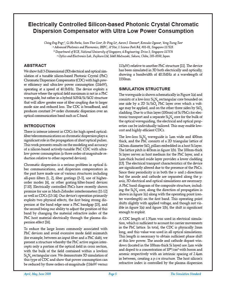
Electrically Controlled Silicon-based Photonic Crystal Chromatic Dispersion Compensator with Ultra Low Power Consumption
We show full 3-Dimensional (3D) electrical and optical simulation of a tunable silicon-based Photonic Crystal (PhC) Chromatic Dispersion Compensator (CDC) with high power efficiency and ultra-low power consumption (114nW), operating at a speed of 40.5MHz. The device exploits a structure where the optical field maximum is not in a PhC waveguide, but rather in a hybrid Si3N4/Si/SiO2 structure that will allow greater ease of fiber coupling due to larger mode size and reduced loss. The CDC is broadband, and produces constant 2nd order chromatic dispersion over an optical communication band such as C-band.

