Simulation Standard
Silvaco面向半导体工艺和器件仿真工程师推出的技术刊物
How to Mesh in 2D TCAD
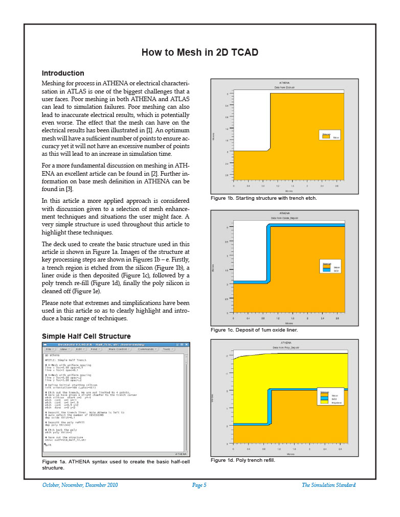
Meshing for process in ATHENA or electrical characterisation in ATLAS is one of the biggest challenges that a user faces. Poor meshing in both ATHENA and ATLAS can lead to simulation failures. Poor meshing can also lead to inaccurate electrical results, which is potentially even worse. The effect that the mesh can have on the electrical results has been illustrated in [1]. An optimum mesh will have a sufficient number of points to ensure accuracy yet it will not have an excessive number of points as this will lead to an increase in simulation time.
Using VICTORY Process for Plasma Etching Simulations
VICTORY Process, the 3D process simulator now includes a module for plasma etching. The module is designed to simulate plasma etching processes at the feature-scale size. The simulation in the reactor-scale region is out of the scope of VICTORY Process. All transport characteristics data (as functions of reactor parameters needed for the feature-scale simulation) are modeled by user definable C-functions and are supplied to the module. The plasma etching simulator shares many elements with the standard physical etching /deposition module such as:
Hints, Tips, and Solutions – Passing a Variable from an ATLAS deck into a C-Interpreter Function
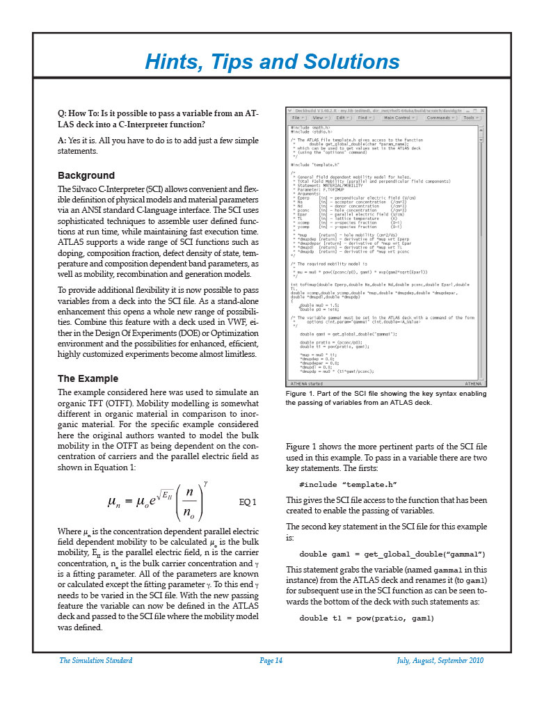
The Silvaco C-Interpreter (SCI) allows convenient and flexible definition of physical models and material parameters via an ANSI standard C-language interface. The SCI uses sophisticated techniques to assemble user defined functions at run time, while maintaining fast execution time. ATLAS supports a wide range of SCI functions such as doping, composition fraction, defect density of state, temperature and composition dependent band parameters, as well as mobility, recombination and generation models.
Simulating Negative Bias Temperature Instability of p-MOSFETS
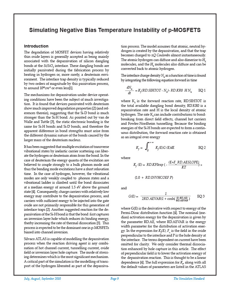
The degradation of MOSFET devices having relatively thin oxide layers is generally accepted as being mainly associated with the depassivation of silicon dangling bonds at the Si/SiO2 interface. These dangling bonds are initially passivated during the fabrication process by heating in hydrogen or, more rarely, a deuterium environment. The interface trap density is typically reduced by two orders of magnitude by this passivation process, to around 1010cm-2 or even less[1].

Coupled Optimization of Diode and IGBT Characteristics Under Clamped Inductive Switching in ATLAS MixedMode and Virtual Wafer Fab (VWF)
Virtual Wafer Fab’s powerful range of optimizers are used to investigate and minimise the coupled switching losses of a TCAD IGBT and its clamping diode in a chopper circuit. It is shown that it is vital that the designer concurrently optimizes both the switching losses of the IGBT and the clamping diode in a single operation.
Using Manual Refinement of Geometrical Mesh in VICTORY Process
VICTORY Process is a 3D process simulation tool which employs the LevelSet technique for manipulating and deforming structures. The structure’s geometry is stored implicitly on the hierarchy of regular (constant mesh size along each direction) Cartesian meshes.

