Guardian-Net Netlist Extractor: An Example of Specific Device Extraction Using XI-Scripts
Guardian LVS from Silvaco is an efficient, reliable, and diverse package that brings the benefit of high-speed verification to PC-based test environments. Guardian netlist extractor, included with the Guardian suite, is a dynamic module that supports the high-speed extraction of a variety of devices, including MOS transistors, resistors, capacitors, and other standard devices.
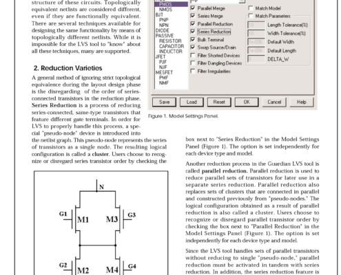
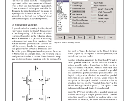
Complex Parallel-Series Reduction
Silvaco’s Guardian LVS tool compares two circuits that are defined by their netlists. The comparison is based strictly on the topological structure of these circuits. Topologically equivalent netlists are considered different, even if they are functionally equivalent. There are several techniques available for designing the same functionality by means of topologically different netlists. While it is impossible for the LVS tool to "know" about all these techniques, many are supported.
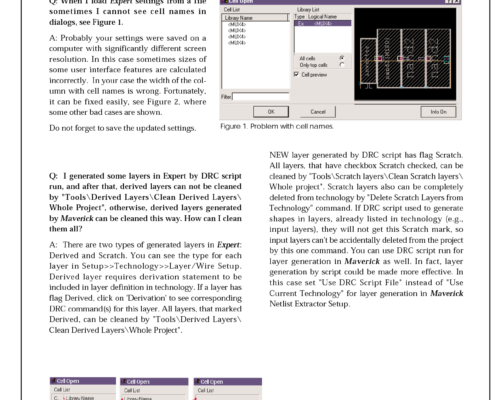
Expert Editor Settings and Layer Cleaning
I generated some layers in Expert by DRC script run, and after that, derived layers can not be cleaned by "Tools\Derived Layers\Clean Derived Layers\ Whole Project", otherwise, derived layers generated by Maverick can be cleaned this way. How can I clean them all?
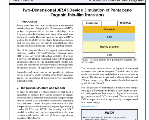
Two-Dimensional ATLAS Device Simulation of Pentacene Organic Thin-film Transistors
Recent years has seen rapid acceleration in the research and development of organic thin film transistors (OTFTs) as key components for active matrix displays, radio frequency identification tags, and many other small scale integrated circuits. There are many advantages to OTFTs, such as the flexibility of the plastic fabrication substrate and the potential cost savings to manufacturers that adopt a solution process and/or ink-jet printing process.
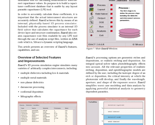
Exact2: Interconnect Parasitic Capacitance Simulator
Exact2 from Silvaco is a sophisticated, physically-based simulation tool for calculating semiconductor interconnect capacitance values. Its purpose is to build a capacitance coefficient database that is usable by any layout parasitic capacitance (LPE) tool.
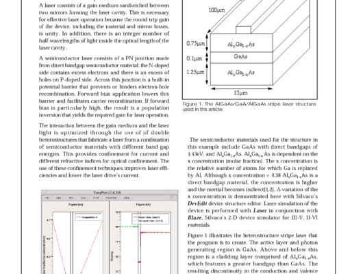
Laser Simulation Encompassing Molar Fraction Variation via DevEdit
This article addresses the creation of semiconductor laser double heterostructures, and the subsequent simulation of laser output with DevEdit from Silvaco. A laser consists of a gain medium sandwiched between two mirrors forming the laser cavity. This is necessary for effective laser operation because the round trip gain of the device, including the material and mirror losses, is unity. In addition, there is an integer number of half-wavelengths of light inside the optical length of the laser cavity.
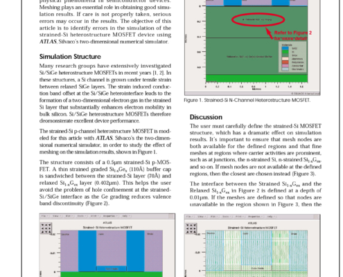
The Importance of Mesh Definition in Strained-Si Heterostructure Simulation
Computer simulation is used extensively to verify physical phenomena in semiconductor devices. Meshing plays an essential role in obtaining good simulation results. If care is not properly taken, serious errors may occur in the results. The objective of this article is to identify errors in the simulation of the strained-Si heterostructure MOSFET device using ATLAS, Silvaco’s two-dimensional numerical simulator.
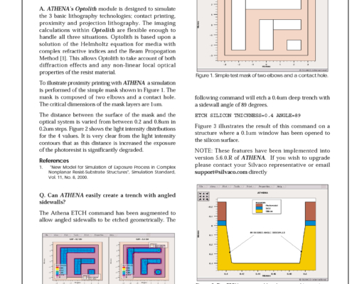
Optical Lithography Models in ATHENA
ATHENA’s Optolith module is designed to simulate the 3 basic lithography technologies; contact printing, proximity and projection lithography. The imaging calculations within Optolith are flexible enough to handle all three situations. Optolith is based upon a solution of the Helmholtz equation for media with complex refractive indices and the Beam Propogation Method [1]. This allows Optolith to take account of both diffraction effects and any non-linear local optical properties of the resist material.
A CAD Framework for Co-Design and Analysis of CMOS-SET Hybrid Integrated Circuits
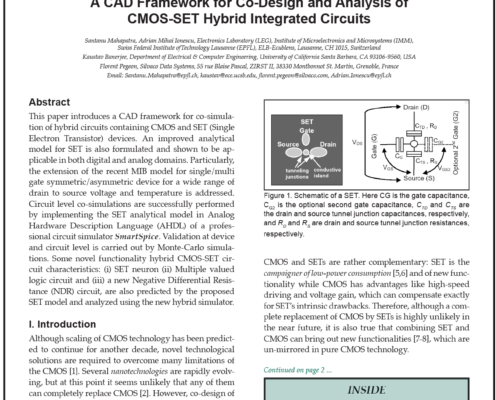
This paper introduces a CAD framework for co-simulation of hybrid circuits containing CMOS and SET (Single Electron Transistor) devices. An improved analytical model for SET is also formulated and shown to be applicable in both digital and analog domains.
Behavioral Modeling and Simulation in the Scholar Schematic Environment
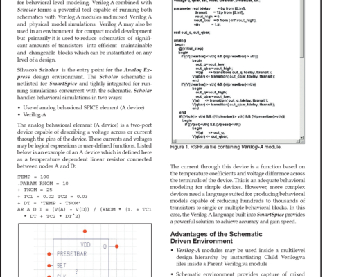
This article focusses on the use of Silvaco International’s schematic capture and editing tool Scholar combined with Verilog A. Verilog A is a standard language used for behavioral level modeling. Verilog A combined with Scholar forms a powerful tool capable of running both schematics with Verilog A modules and mixed Verilog A and physical model simulations. Verilog A may also be used in an environment for compact model development but primarily it is used to reduce schematics of significant amounts of transistors into efficient maintainable and changeable blocks which can be instantiated on any level of a design.
