
Simulation Standard
Silvaco面向半导体工艺和器件仿真工程师推出的技术刊物
 https://silvaco.com/wp-content/uploads/2020/10/simstd_Q3_2020_a2.jpg
719
546
Erick Castellon
/wp-content/uploads/2019/11/silvaco-logo.png
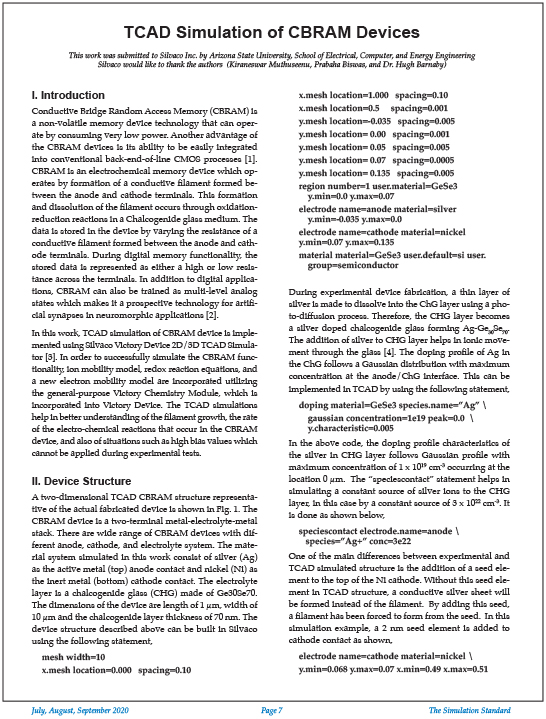
Erick Castellon2020-10-01 00:04:372021-09-22 13:50:48TCAD Simulation of CBRAM Devices
https://silvaco.com/wp-content/uploads/2020/10/simstd_Q3_2020_a2.jpg
719
546
Erick Castellon
/wp-content/uploads/2019/11/silvaco-logo.png
Erick Castellon2020-10-01 00:04:372021-09-22 13:50:48TCAD Simulation of CBRAM Devices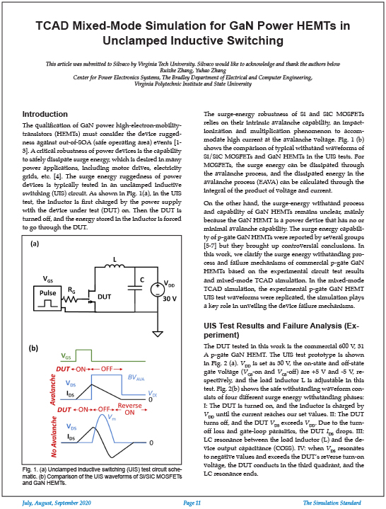 https://silvaco.com/wp-content/uploads/2020/10/simstd_Q3_2020_a3.jpg
719
546
Erick Castellon
/wp-content/uploads/2019/11/silvaco-logo.png
Erick Castellon2020-10-01 00:03:042021-09-22 13:50:48TCAD Mixed-Mode Simulation for GaN Power HEMTs in Unclamped Inductive Switching
https://silvaco.com/wp-content/uploads/2020/10/simstd_Q3_2020_a3.jpg
719
546
Erick Castellon
/wp-content/uploads/2019/11/silvaco-logo.png
Erick Castellon2020-10-01 00:03:042021-09-22 13:50:48TCAD Mixed-Mode Simulation for GaN Power HEMTs in Unclamped Inductive Switching https://silvaco.com/wp-content/uploads/2020/10/simstd_Q3_2020_hints.jpg
719
554
Erick Castellon
/wp-content/uploads/2019/11/silvaco-logo.png
Erick Castellon2020-10-01 00:02:522021-09-22 13:50:48Using Victory Process Open Model Interface to Customize Etch Emulation Model – Example
https://silvaco.com/wp-content/uploads/2020/10/simstd_Q3_2020_hints.jpg
719
554
Erick Castellon
/wp-content/uploads/2019/11/silvaco-logo.png
Erick Castellon2020-10-01 00:02:522021-09-22 13:50:48Using Victory Process Open Model Interface to Customize Etch Emulation Model – Example https://silvaco.com/wp-content/uploads/2020/07/VP_Figure3b.png
889
966
Erick Castellon
/wp-content/uploads/2019/11/silvaco-logo.png
Erick Castellon2020-07-31 04:51:532021-09-22 13:51:062020 TCAD Baseline Release Section 1: Process Simulation – New Features in 2020 Baseline Release
https://silvaco.com/wp-content/uploads/2020/07/VP_Figure3b.png
889
966
Erick Castellon
/wp-content/uploads/2019/11/silvaco-logo.png
Erick Castellon2020-07-31 04:51:532021-09-22 13:51:062020 TCAD Baseline Release Section 1: Process Simulation – New Features in 2020 Baseline Release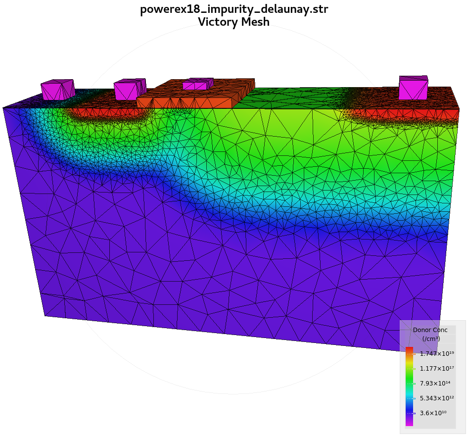 https://silvaco.com/wp-content/uploads/2020/07/Mesh_Figure3b.png
881
946
Erick Castellon
/wp-content/uploads/2019/11/silvaco-logo.png
Erick Castellon2020-07-31 04:34:592021-09-22 13:51:062020 TCAD Baseline Release Section 2: Meshing – New Features in 2020 Baseline Release
https://silvaco.com/wp-content/uploads/2020/07/Mesh_Figure3b.png
881
946
Erick Castellon
/wp-content/uploads/2019/11/silvaco-logo.png
Erick Castellon2020-07-31 04:34:592021-09-22 13:51:062020 TCAD Baseline Release Section 2: Meshing – New Features in 2020 Baseline Release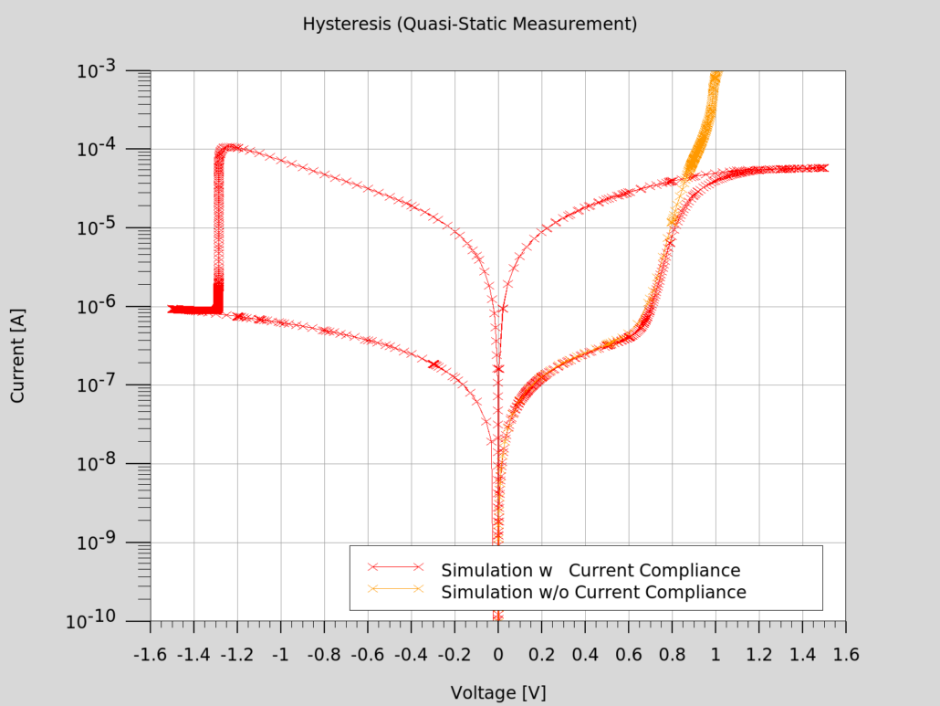 https://silvaco.com/wp-content/uploads/2020/07/reram_fig1.png
1200
1600
Erick Castellon
/wp-content/uploads/2019/11/silvaco-logo.png
Erick Castellon2020-07-31 04:25:342021-09-22 13:51:062020 TCAD Baseline Release – Device Simulation – New Features in 2020 Baseline Release
https://silvaco.com/wp-content/uploads/2020/07/reram_fig1.png
1200
1600
Erick Castellon
/wp-content/uploads/2019/11/silvaco-logo.png
Erick Castellon2020-07-31 04:25:342021-09-22 13:51:062020 TCAD Baseline Release – Device Simulation – New Features in 2020 Baseline Release