Hints, Tips and Solutions – Meshing a Non Axis Aligned SEU Beam
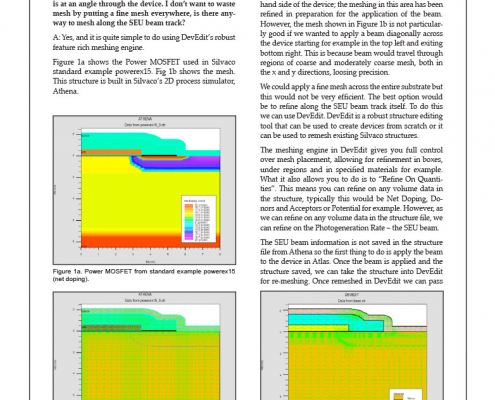
Q: I have an SEU beam in a 2D structure; the beam track is at an angle through the device. I don’t want to waste mesh by putting a fine mesh everywhere, is there anyway to mesh along the SEU beam track?
A: Yes, and it is quite simple to do using DevEdit’s robust feature rich meshing engine.
Hints, Tips, and Solutions – Calculate Light Extraction Efficiency in an OLED or LED with Pure Optical Simulation
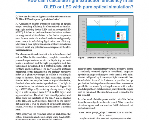
Calculation of light extraction efficiency or optical output coupling efficiency is often needed in simulating a light emitting device (LED) such as an organic LED (OLED). It is best to perform these calculations without running electrical simulation in the device, as parameters for new materials are hard to obtain and generally unnecessary in calculating light extraction efficiency. Moreover, a pure optical simulation will save simulation time and avoid any potential un-convergence in the electrical simulation.
Hints, Tips, and Solutions – Achieve Publication Quality Plots Using TonyPlot
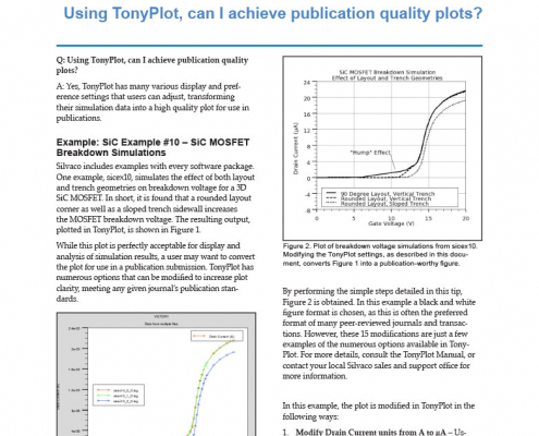
Yes, TonyPlot has many various display and preference settings that users can adjust, transforming their simulation data into a high quality plot for use in publications.
Simulations of Deep-Level Transient Spectroscopy for 4H-SiC
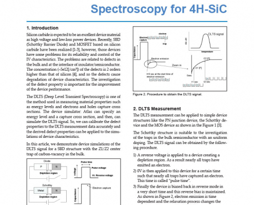
Silicon carbide is expected to be an excellent device material as high voltage and low-loss power devices. Recently, SBD (Schottky Barrier Diode) and MOSFET based on silicon carbide have been realized [1-3], however, those devices have some problems for its reliability and control of the IV characteristics. The problems are related to defects in the bulk and at the interface of insulator/semiconductor. The concentration (~5e12[/cm3]) of the defects is 2 orders higher than that of silicon [4], and so the defects cause degradation of device characteristics. The investigation of the defect property is important for the improvement of the device performance.
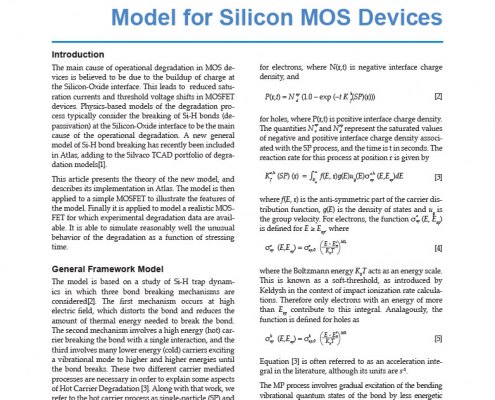
Generally Applicable Degradation Model for Silicon MOS Devices
The main cause of operational degradation in MOS devices is believed to be due to the buildup of charge at the Silicon-Oxide interface. This leads to reduced saturation currents and threshold voltage shifts in MOSFET devices. Physics-based models of the degradation process typically consider the breaking of Si-H bonds (depassivation) at the Silicon-Oxide interface to be the main cause of the operational degradation. A new general model of Si-H bond breaking has recently been included in Atlas, adding to the Silvaco TCAD portfolio of degradation models[1].
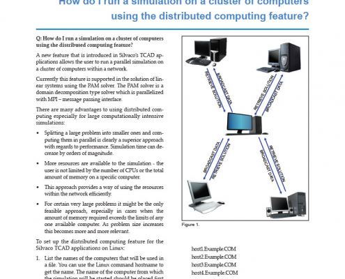
Hints, Tips, and Solutions – Simulation on a Cluster of Computers Using the Distributed Computing Feature
A new feature that is introduced in Silvaco’s TCAD applications allows the user to run a parallel simulation on a cluster of computers within a network.
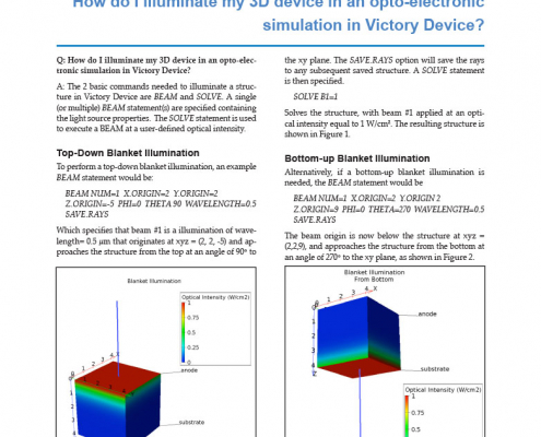
Hints, Tips and Solutions – Illuminate a 3D device in a Victory Device Opto-electronic Simulation
A: The 2 basic commands needed to illuminate a structure in Victory Device are BEAM and SOLVE. A single (or multiple) BEAM statement(s) are specified containing the light source properties. The SOLVE statement is used to execute a BEAM at a user-defined optical intensity.
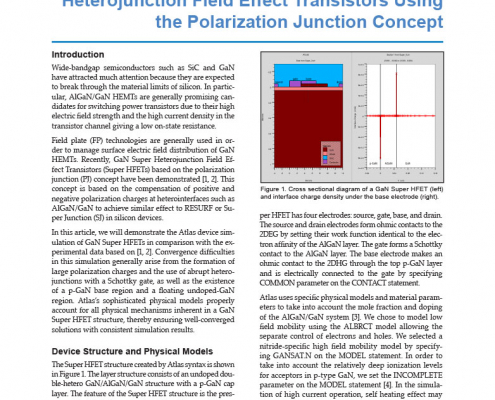
Atlas Simulation of GaN-Based Super Heterojunction Field Effect Transistors Using the Polarization Junction Concept
Wide-bandgap semiconductors such as SiC and GaN have attracted much attention because they are expected to break through the material limits of silicon. In particular, AlGaN/GaN HEMTs are generally promising candidates for switching power transistors due to their high electric field strength and the high current density in the transistor channel giving a low on-state resistance.
Modeling the Optical Response of Phonon-dressed Excitons in OLED Simulations
We demonstrate the modeling of optical response of exciton-polarons based on the well established Holstein Hamiltonian to model coupled exciton-phonon systems in organic molecular chains. Our approach uses Green’s functions to compute the density of states and the linear optical susceptibility, and thus eliminates the conventional and computationally expensive step of diagonalizing a large Hamiltonian matrix. We exploit this technique further to focus exclusively on the optically active states when computing the linear optical response, and significantly reduce the computational effort to construct the optical susceptibility. In this article, we demonstrate the computation of absorption and emission spectra of Alq3 at 4.2 K and at room temperature using our model. Using the two parameters of the Holstein model, the inhomogeneous broadening energies, and a phenomenological reorganization energy of the solute, we obtain excellent fits to established experimental results. We then use this model inside the larger simulation of a 3-layer organic light emitting (OLED) structure composed of Alq3, Alq3:DCJTB, and α-NPD, which are the electron transport, emissive, and hole transport layers respectively. In our methodology, we also couple the optical response into the rate equations for exciton dynamics in addition to computing the spectrum of light output by the device.
Hints, Tips, and Solutions – Simulate Rapid Thermal Annealing Temperature Transients in Vacuum
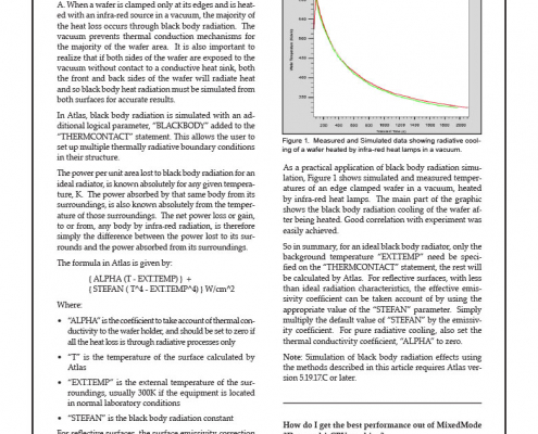
When a wafer is clamped only at its edges and is heated with an infra-red source in a vacuum, the majority of the heat loss occurs through black body radiation. The vacuum prevents thermal conduction mechanisms for the majority of the wafer area. It is also important to realize that if both sides of the wafer are exposed to the vacuum without contact to a conductive heat sink, both the front and back sides of the wafer will radiate heat and so black body heat radiation must be simulated from both surfaces for accurate results.
