Mocasim – A Versatile Monte Carlo Simulator for III-Nitride Transport Properties
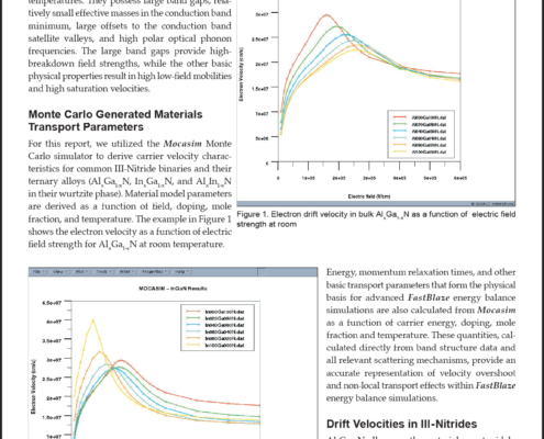
III-Nitrides have recently attracted attention as a promising material class for high-power, high-frequency microelectronic applications at elevated temperatures. They possess large band gaps, relatively small effective masses in the conduction band minimum, large offsets to the conduction band satellite valleys, and high polar optical phonon frequencies. The large band gaps provide high-breakdown field strengths, while the other basic physical properties result in high low-field mobilities and high saturation velocities.
Schrödinger Approach and Density Gradient Model for Quantum Effects Modeling
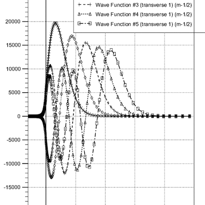
We describe here two approaches to model the quantum effects that can no more be neglected in actual and future devices. These models are the Schrödinger-Poisson and Density-Gradient methods fully integrated in the device simulator ATLAS. Simulations based on such methods are compared to each other on electron concentration and C-V curves in a MOS-capacitor.
How can I use the EXTRACT commands to find the depletion widths in my MOSFET at different drain biases?
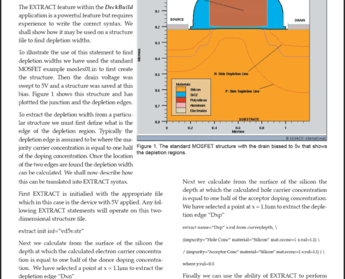
To illustrate the use of this statement to find depletion widths we have used the standard MOSFET example mos1ex01.in to first create the structure. Then the drain voltage was swept to 5V and a structure was saved at this bias. Figure 1 shows this structure and has plottted the junction and the depletion edges.
Instructional Approach to Writing Parasitic Capacitance Rules Files Using Exact
1. Introduction
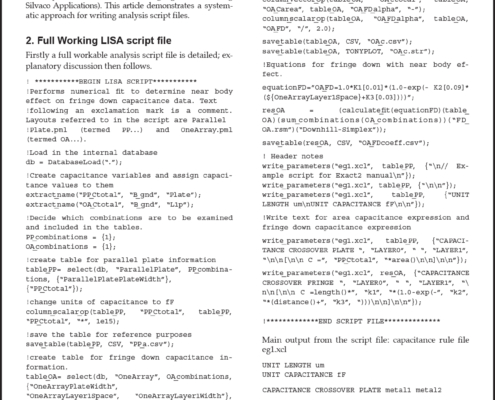
The Exact analysis stage extracts the user-required information necessary for the respective parasitic capacitances by probing the Exact database. This is performed via script files written in LISA (Language for Interfacing Silvaco Applications). This article demonstrates a systematic approach for writing analysis script files.
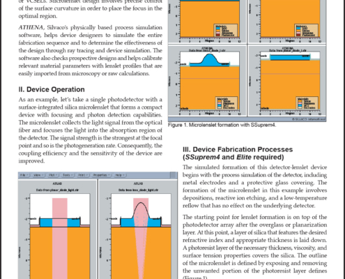
Simulation of Silica Microlenslet Formation by Etch and Reflow Using Elite and SSuprem4
Introduction
In response to high demand, device designers are developing silica microlenslets that offer efficient coupling between optical fiber bundles and arrays of photodetectors, LEDs, or VCSELs. Microlenslet design involves precise control of the surface curvature in order to place the focus in the optimal region.
Remote ALTER processing
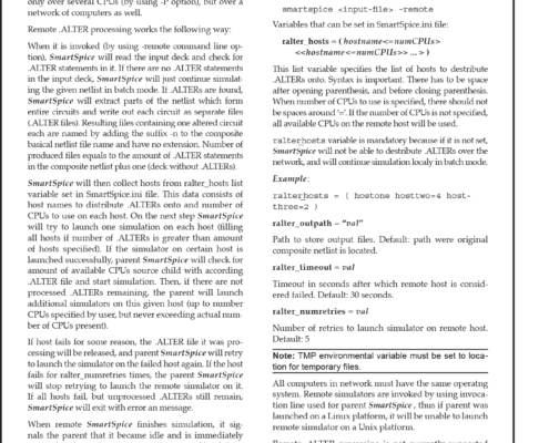
A new parallelization method has been implemented into SmartSpice. Now .ALTERs can be destributed not only over several CPUs (by using -P option), but over a network of computers as well.
Remote .ALTER processing works the following way:
When it is invoked (by using -remote command line option), SmartSpice will read the input deck and check for .ALTER statements in it. If there are no .ALTER statements in the input deck, SmartSpice will just continue simulating the given netlist in batch mode. If .ALTERs are found, SmartSpice will extract parts of the netlist which form entire circuits and write out each circuit as separate files (.ALTER files). Resulting files containing one altered circuit each are named by adding the suffix -n to the composite basical netlist file name and have no extension. Number of produced files equals to the amount of .ALTER statements in the composite netlist plus one (deck without .ALTERs).
New SmartLIb Library of Models
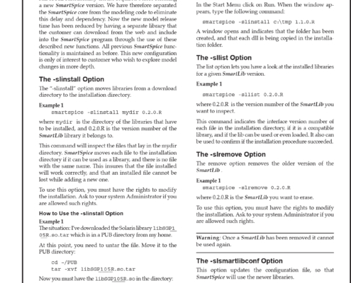
In all previous versions of SmartSpice the model code (BSIM, diode etc.) was included in the one executable (SmartSpice ). This means any updates to the model code would take a while to reach the customer because of the full SPICE functionality checks required before releasing a new SmartSpice version.
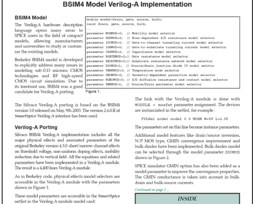
BSIM4 Model Verilog-A Implementation
The Verilog-A hardware description language opens many areas to SPICE users in the field of compact models, allowing manufacturers and universities to study or customize the existing models.
Stress Effect Model in BSIM3v3 Model
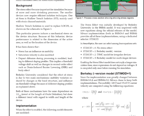
Stress effect models are now implemented in major models such as BSIM4 or HiSIM. The need for evermore accurate models with a strong relation to technology is accute. Since BSIM3v3 is still a widely-used model and has not been totally replaced by its successor, an improvement was made to the model in SmartSpice to fulfill customers need for stress effect equations.
New Philips MOS20 LDMOS Model in SmartSpice
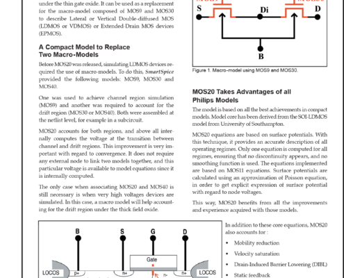
Philips MOS20 was released in January 2004. Its purpose is to provide a high-voltage compact model to describe both operation of the channel region and drift region under the thin gate oxide.
