Numerical Analysis of GaInP Solar Cells: Toward Advanced Photovoltaic Devices Modeling
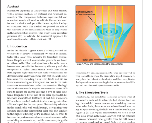
Simulation capacities of GaInP solar cells were studied with a special emphasis on material and structural parameters. The comparison between experimental and numerical results allowed to validate the models used for such a device and permitted to extrapolate the layers structure. With this method we proved the role of the substrate in the simulation and thus its importance in the optimization process. This study is an important previous step to validate the numerical approach for multi-junction solar cell simulation in 3D.

Simulation and Characterization of High-Frequency Performances of Advanced MIM Capacitors
Abstract:
High-frequency simulations and characterizations of advanced metal-insulator-metal (MIM) capacitors with ultra thin 32 nm PECVD Si3N4 dielectric are presented. The frequency dependent behavior of capacitors is numerically and experimentally extracted over a wide frequency bandwidth. Numerical results are validated by comparison to experimental results. An equivalent circuit model of capacitors including four parameters is developed for a better understanding of the frequency dependent behavior. We focused on the impact of design on the performances of MIM capacitors realized on Si substrates.
How can I create a Design Of Experiments (DOE) using DeckBuild with one or more variables
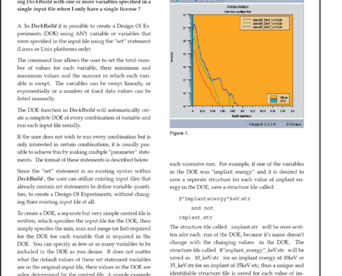
How can I create a Design Of Experiments (DOE) using DeckBuild with one or more variables specified in a single input file when I only have a single license?
Process Flow Simulation and Manufacture of Variable RF MEMS Capacitors
Introduction
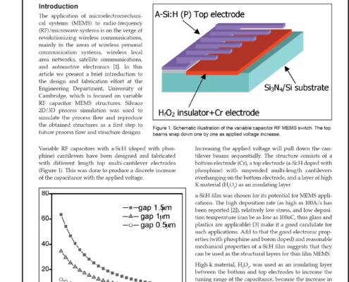
The application of microelectromechanical systems (MEMS) to radio-frequency (RF)/microwave systems is on the verge of revolutionizing wireless communications, mainly in the areas of wireless personal communication systems, wireless local area networks, satellite communications, and automotive electronics [1]. In this article we present a brief introduction to the design and fabrication effort at the Engineering Department, University of Cambridge, which is focused on variable RF capacitor MEMS structures. Silvaco 2D/3D process simulation was used to simulate the process flow and reproduce the obtained structures as a first step to future process flow and structure designs.
Gate Charging Simulation Using Atlas/MixedMode
Introduction
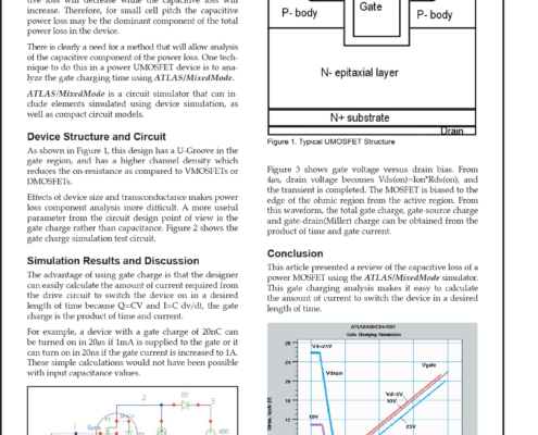
In modern power devices, the total power loss comprises both a conductive power loss component and a capacitive loss component. As the cell pitch decreases, the conductive loss will decrease while the capacitive loss will increase. Therefore, for small cell pitch the capacitive power loss may be the dominant component of the total power loss in the device.
Using Athena Monte Carlo Module for Ion Implantation Simulation in Silicon Carbides
Introduction
The Monte Carlo Implantation Module of ATHENA has proved to be a very accurate tool for simulation of various implantation processes. In this paper we demonstrate that the module can be successfully used not only for classical silicon-based technologies but also for other materials used in semiconductor industry. Silicon carbides were selected for this demonstration not only because they are widely used in power and high frequency electronics but also because they are most challenging objects for simulation due to their complicated lattice structures and electronic stopping models.
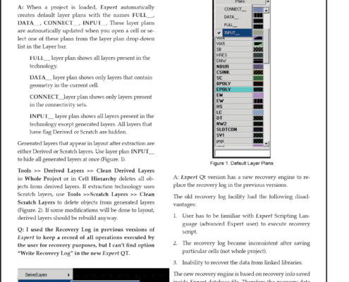
Is there a way to turn-off all of the generated layers
Is there a way to turn-off all of the generated layers so that the layout modifications can be done without them cluttering things?
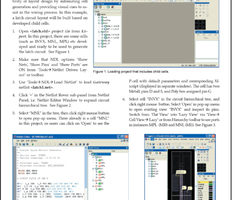
Expert’s Netlist Driven Layout
Expert features a powerful Netlist Driven Layout (NDL) function to assist the user in creating a layout. It increases the productivity of layout design by automating cell generation and providing visual cues to assist in the wiring process. In this example, a latch circuit layout will be built based on developed child cells.
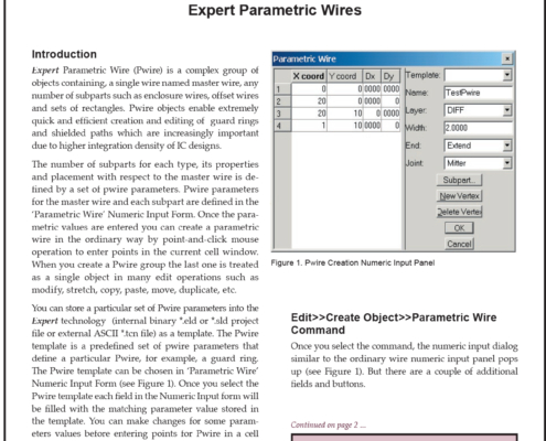
Expert Parametric Wires
Expert Parametric Wire (Pwire) is a complex group of objects containing, a single wire named master wire, any number of subparts such as enclosure wires, offset wires and sets of rectangles. Pwire objects enable extremely quick and efficient creation and editing of guard rings and shielded paths which are increasingly important due to higher integration density of IC designs.
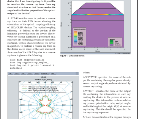
I am currently using ATLAS/ Blaze to model the electrical properties of an LED device
I am currently using ATLAS/ Blaze to model the electrical properties of an LED device that I am investigating. Is it possible to examine the reverse ray trace from my simulated structure so that I can examine the angular distribution properties of the optical output of the device?
